EP4357743B1 - Procédé de surveillance de la fiabilité d'un système comprenant des composants électriques - Google Patents
Procédé de surveillance de la fiabilité d'un système comprenant des composants électriques Download PDFInfo
- Publication number
- EP4357743B1 EP4357743B1 EP22203094.2A EP22203094A EP4357743B1 EP 4357743 B1 EP4357743 B1 EP 4357743B1 EP 22203094 A EP22203094 A EP 22203094A EP 4357743 B1 EP4357743 B1 EP 4357743B1
- Authority
- EP
- European Patent Office
- Prior art keywords
- electrical component
- electrical
- temperature
- ecn
- value
- Prior art date
- Legal status (The legal status is an assumption and is not a legal conclusion. Google has not performed a legal analysis and makes no representation as to the accuracy of the status listed.)
- Active
Links
Images


Classifications
-
- G—PHYSICS
- G01—MEASURING; TESTING
- G01R—MEASURING ELECTRIC VARIABLES; MEASURING MAGNETIC VARIABLES
- G01R31/00—Arrangements for testing electric properties; Arrangements for locating electric faults; Arrangements for electrical testing characterised by what is being tested not provided for elsewhere
-
- G—PHYSICS
- G01—MEASURING; TESTING
- G01K—MEASURING TEMPERATURE; MEASURING QUANTITY OF HEAT; THERMALLY-SENSITIVE ELEMENTS NOT OTHERWISE PROVIDED FOR
- G01K7/00—Measuring temperature based on the use of electric or magnetic elements directly sensitive to heat ; Power supply therefor, e.g. using thermoelectric elements
- G01K7/42—Circuits effecting compensation of thermal inertia; Circuits for predicting the stationary value of a temperature
-
- G—PHYSICS
- G01—MEASURING; TESTING
- G01R—MEASURING ELECTRIC VARIABLES; MEASURING MAGNETIC VARIABLES
- G01R31/00—Arrangements for testing electric properties; Arrangements for locating electric faults; Arrangements for electrical testing characterised by what is being tested not provided for elsewhere
- G01R31/26—Testing of individual semiconductor devices
- G01R31/2607—Circuits therefor
- G01R31/2621—Circuits therefor for testing field effect transistors, i.e. FET's
- G01R31/2628—Circuits therefor for testing field effect transistors, i.e. FET's for measuring thermal properties thereof
-
- G—PHYSICS
- G01—MEASURING; TESTING
- G01K—MEASURING TEMPERATURE; MEASURING QUANTITY OF HEAT; THERMALLY-SENSITIVE ELEMENTS NOT OTHERWISE PROVIDED FOR
- G01K3/00—Thermometers giving results other than momentary value of temperature
- G01K3/005—Circuits arrangements for indicating a predetermined temperature
-
- G—PHYSICS
- G01—MEASURING; TESTING
- G01R—MEASURING ELECTRIC VARIABLES; MEASURING MAGNETIC VARIABLES
- G01R31/00—Arrangements for testing electric properties; Arrangements for locating electric faults; Arrangements for electrical testing characterised by what is being tested not provided for elsewhere
- G01R31/003—Environmental or reliability tests
-
- G—PHYSICS
- G01—MEASURING; TESTING
- G01R—MEASURING ELECTRIC VARIABLES; MEASURING MAGNETIC VARIABLES
- G01R31/00—Arrangements for testing electric properties; Arrangements for locating electric faults; Arrangements for electrical testing characterised by what is being tested not provided for elsewhere
- G01R31/005—Testing of electric installations on transport means
-
- G—PHYSICS
- G01—MEASURING; TESTING
- G01K—MEASURING TEMPERATURE; MEASURING QUANTITY OF HEAT; THERMALLY-SENSITIVE ELEMENTS NOT OTHERWISE PROVIDED FOR
- G01K3/00—Thermometers giving results other than momentary value of temperature
- G01K3/08—Thermometers giving results other than momentary value of temperature giving differences of values; giving differentiated values
Definitions
- the present disclosure relates to the field of monitoring reliability of a system including one or more electrical components, for example a system including a transistor, such a MOSFET, used as a switch to power on or off a load from a power source.
- a system including a transistor such as a MOSFET, used as a switch to power on or off a load from a power source.
- a transistor such as a MOSFET may be used as a switch to power on or off a load from a power source.
- the MOSFETs are likely to have failures in use. These failures are often attributed to over voltage, over current, over temperature etc... In operation, the temperature of the transistor may increase. When a critical temperature is reached, the transistor should be turned off to avoid any damage.
- an intelligent MOSFET including a temperature protection circuitry normally present on a printed circuit board on which the MOSFET is mounted.
- a temperature sensor is sitting on a die or semiconductor part of the MOSFET. This temperature sensor can measure very fast the temperature. If the temperature sensor is alternatively mounted on the PCB, a fast temperature increase cannot be detected.
- the present disclosure concerns a method of monitoring reliability of a system according to claim 1.
- the present disclosure also concerns:
- a particular embodiment of the system 100 is illustrated in figure 1 and includes a transistor EC1 having the function of switching on or off a load 300 from a power source 500, and an interface connecting the transistor EC 1 to the load 300.
- the transistor EC1 may be a FET, for example a MOSFET.
- the interface may include an electrical shunt EC2, for example a copper shunt, and an electrical cable EC3.
- the transistor EC1 may be mounted on a printed circuit board, the copper shunt EC2 may be a copper track of the PCB, 400.
- the electrical cable EC3 may be external to the printed circuit board 400 and connect the shunt EC2 and the load 300.
- the temperature of the electrical components ECn of the system 100 may vary over time, for example due to power loss.
- the present method allows to determine a temperature information of the electrical components ECn of the system 100 and monitor the reliability of these electrical components ECn using the determined temperature information.
- the temperature information is determined by processing input data, that includes electrical characteristics of the electrical component ECn, using a stored thermal model representing heat transfer for the electrical component ECn.
- the electrical characteristics of the electrical component ECn used as input data to determine the temperature information of said electrical component ECn can comprise a voltage across the electrical component ECn, a current flowing through the electrical component ECn, and/or an electrical resistance value of the electrical component ECn.
- the thermal model related to an electrical component ECn having an electrical power consumption P n represents heat transfer for said electrical component ECn.
- the heat transfer refers to the heat flow between two given points including a first point of the electrical component ECn, where the temperature is to be estimated, and a second point, where a temperature referred as a reference or ambient temperature Ta is known, for example by measurement.
- the second point is for example a point of the printed circuit board 400 on which a temperature sensor 410 is mounted.
- the ambient temperature Ta may be the air temperature around the cable EC3.
- the thermal model is a Cauer thermal model, for example a first order Cauer thermal model having a simple structure as represented by an equivalent circuit in figure 2 , including a thermal capacitance Cth n and a thermal resistance Rth n of the electrical component ECn, both connected in parallel between a power supply point, provided with the electrical power P n , and the ground.
- the thermal resistance Rth n is a quantification of how difficult it is for heat to be conducted between the two given points.
- the thermal capacitance Cth n is a quantification of how quickly heat is conducted between the two given points.
- the thermal modal could be a Cauer model with higher order. In that case, the Cauer model just needs additional calculations after first order is determined.
- the electrical power P n consumed or dissipated by the electrical component EC n can be determined from measurements of a voltage V n across the electrical component and/or a current I n flowing through the electrical component ECn.
- the time step dt may be of the order of a few hundred microseconds.
- a temperature information of the electrical component ECn such as a temperature variation or difference relative to the reference or ambient temperature Ta can be determined using the thermal model.
- the temperature Ta may be measured by a sensor near the electrical component ECn, for example the temperature sensor 410 mounted on the printed circuit board 400.
- thermal modal Any other type of thermal modal could be used for modelling heat transfer through the electrical component.
- the electrical resistance value of an electrical component ECn may vary over time due to a temperature variation of this electrical component ECn. Consequently, an electrical current flowing through this electrical component ECn may vary over time.
- the present method allows to determine and update over time the values of electrical characteristics of the system 100 that are temperature dependent, as explained later in more detail.
- the method of monitoring reliability of the system 100 may be carried out by a monitoring device 200.
- the monitoring device 200 is mounted on the printed circuit board 400.
- the monitoring device 200 includes an input interface 205, a measurement module 210, a memory system 220, a processing module 230, and a diagnostic module 240.
- the monitoring device 200 may also include a controlling module 250 configured to control the transistor EC1.
- the monitoring device 200 may be implemented with hardware and software.
- the monitoring device 200 may include a processor, not represented in figure 1 , and software or computer programs or applications configured to run on the processor.
- the input interface 205 is a user interface configured to exchange information between the system 100 and a user, and to switch on and off the transistor EC1.
- the measurement module 210 is configured to measure voltage across the transistor EC1 and across the shunt EC2 and acquire the temperature measured by the temperature sensor 410.
- the measurement module 210 may include one or more amplifier(s) to amplify low measurement values to higher values, and one or more analog to digital converter(s) to convert analog measured values to digital data and transmit the digital data to the memory system 220.
- the memory system 220 may include:
- the processing module 230 is configured to receive or acquire input data including electrical characteristics of the electrical components ECn of the system 100.
- the processing module 230 is further configured to process said input data using stored thermal models representing heat transfer for the electrical components ECn respectively, to determine a temperature information of the electrical components ECn.
- the processing module may further be configured to determine temperature-dependent electrical characteristics of the electrical components ECn, such as a resistance and/or a current, using the determined temperature information.
- the processing module 230 may include a processor.
- the diagnostic module 240 is configured to monitor the reliability of the system 100 using the determined temperature information of the electrical components ECn and/or the electrical characteristics of the electrical components ECn determined based on the determined temperature information, as will be described in more detail in the description of the method.
- FIG. 3 An embodiment of the method of monitoring reliability of one or more electrical components ECn of the system 100 is illustrated in figure 3 and will now be described. The method is performed by the monitoring device 200.
- the method may include an iterative process performed at successive times t 1 , t 2 , t 3 , ..., or sampling times, for the electrical component ECn.
- the iterative process includes:
- the steps S1 and S2 can be performed by the processing module 230.
- the processing module 230 receives or acquires input data.
- the input data includes electrical characteristics of the electrical component ECn.
- the electrical characteristics of the electrical component ECn may include a voltage V n (t i ) across the electrical component ECn, and/or a current I n (t i ) flowing through the electrical component ECn.
- the voltage V n (t i ) across the electrical component ECn or the current I n (t i ) flowing through the electrical component ECn may be obtained by or derived from measurement performed at time t i .
- the voltage V n (t i ), or current I n (t i ), of the electrical component ECn is measured by the measurement module 210 and transmitted to the monitoring device 200.
- the current I n (t i ) flowing through the electrical component ECn is estimated by first performing the iterative process including the steps S1 and S2 for another electrical component ECn' of the system 100, based on a temperature information of ECn'.
- the current flowing through the transistor EC1 and the cable EC3 can be first estimated through the shunt EC2, based on a temperature information of the shunt EC2 determined by performing the iterative process S1-S2 for the shunt EC2, as described later in more detail.
- the input data may further include a value of an electrical resistance R n (t i ) of the electrical component ECn.
- the value of the electrical resistance R n (t i ) used as input data at each iteration of the process can correspond to the value of the electrical resistance R n (t i-1 ) determined at the previous iteration of the process, as explained later in more detail.
- the input data may further include an ambient temperature Ta near the electrical component ECn.
- This ambient temperature Ta may be measured at each time t i by a sensor near the electrical component ECn, such as the temperature sensor 410 mounted on the printed circuit board 400, and transmitted to the monitoring device 200 in the step S1, via the measurement module 210.
- this ambient temperature Ta may be set to a maximal ambient temperature that can be expected, prestored in the nonvolatile memory of the memory system 220. In that case, the processing module 220 retrieves from memory the ambient temperature Ta in the step S1.
- the input data may further include prestored constant values of thermal and/or electrical parameters of the electrical component ECn, such as the thermal resistance Rth and thermal capacitance Cth of the material responsible for heat transfer for the electrical component ECn, a temperature coefficient ⁇ n of the electrical component ECn, and a reference electrical resistance value of the electrical component ECn at room temperature, for example 20°C.
- the temperature coefficient ⁇ n of the electrical component ECn represents a temperature dependency of the electrical resistance of the electrical component ECn.
- the processing module 230 processes the input data using the stored thermal model representing heat transfer for the electrical component ECn to determine a temperature information of the electrical component ECn.
- the temperature information may include an estimated variation or difference of temperature between a temperature of the electrical component ECn and the ambient temperature Ta, and/or an estimated temperature of the electrical component ECn.
- the processing step S2 may comprise at least part of the steps S20 to S27 described below.
- the step S2 may comprise a step S20 of evaluating the electrical power P n (t i ) dissipated by the electrical component ECn during the current time step dt, by processing the input data acquired at the step S1, based on one of the equations (1) to (3).
- the processing module 230 may compute the value ⁇ T n,i ( t i ) of incremental temperature variation of the electrical component ECn relative to the ambient temperature Ta over the current time step dt, between times t i and t i+1 , based on the thermal model, for example with the equation (4).
- the step S2 may further comprise a step S22 of determining the value dT n,i of cumulated or global temperature variation of the electrical component ECn relative to the ambient temperature Ta between the initial time t 0 and the current time t i , based on the equation (5).
- the iterative step S22 allows to accumulate successive values of incremental temperature variation of the electrical component ECn relative to the ambient temperature Ta.
- the processing step S2 further includes a step S24 of estimating an electrical resistance value of the electrical component ECn at time t i , based on a predetermined reference electrical resistance value R ref,n of the electrical component ECn, a predetermined temperature coefficient ⁇ n of the electrical component ECn, the ambient temperature Ta and the value dT n,i of temperature difference of the electrical component ECn determined at the step S22.
- the reference electrical resistance value R ref,n may be the electrical resistance value of the electrical component ECn at room temperature, for example 20°C.
- the temperature coefficient ⁇ n is a predetermined constant parameter of the electrical component ECn.
- the parameters R ref,n and ⁇ n are pre-stored in the memory system 220.
- the electrical resistance value R n ( t i ) of the electrical component ECn determined at the iteration of time t i can be used at the next iteration of time t i+1 to estimate the power dissipated by the component ECn based on the equation (1) or (3).
- the current flowing through the electrical component ECn can be averaged over a time window or cycle including N iterations of the process, and having a length N*dt (in other words, over N successive time steps dt).
- an average value of the current I n ( t i ) may be determined periodically or cyclically, every N iterations of the process, here at time t N , t 2N , t 3N , ..., each cycle including N consecutive iterations of the step S25.
- the current I n ( t i ) can be summed up until the N iterations of the step S25 of the cycle have been executed, in other words over N successive iterations.
- a step S26 the sum of the N successive current values estimated in the step S25 over said N iterations is divided by N to determine the averaged current I n ⁇ .
- the average current is updated every N measurements, or every N iterations of the process.
- Averaging allows to reduce noise.
- the current value may be more accurate with averaging.
- the estimated value of the electrical current I n or I n ⁇ flowing through the electrical component ECn can be used as input data in the steps S1 and S2 for another electrical component having the same electrical current flowing through it.
- the output data of the processing step S2 performed for the electrical component ECn may include at least part of the following values :
- the output of the processing step S2 at time t i may be used as input data for the processing step S2 performed at time t i+1 .
- the method further includes a step S3 of monitoring the reliability of the electrical component ECn based on the output data of the processing step S2.
- the step S3 can be performed by the diagnostic module 240.
- One or more pieces of the output data of the processing step S2 may be compared to threshold values prestored for example in the non-volatile memory of the memory system 220 to detect an abnormality in the system 100.
- the detected abnormalities may include for example:
- a step of turning off the system 100, or at least one electrical component of the system 100, and/or triggering an alert may be performed, in a step S4.
- the iterative process including the steps S1 and S2 is performed at successive times t i , every time step dt, and for each electrical component ECn of the system 100 that is monitored.
- the process performed for each of the electrical components of the system in figure 1 including the transistor EC1, the shunt EC2, and the cable EC3, will now be described. It includes, for each component EC1, EC2 or EC3, the steps of the method previously described and illustrated in figure 3 .
- the method steps will be denoted with the suffix _EC1, or _EC2, or _EC3, corresponding to the component for which the method is implemented.
- the process is first performed for the shunt EC2 to estimate the current flowing through the transistor EC1, the shunt EC2 and the cable EC3.
- the estimated current is then used as an input data in the process performed for the transistor EC1 and the cable EC3.
- the shunt EC2 is mounted on the printed circuit board 400. It is a kind of track, for example made of copper.
- the shunt EC2 is a device used to measure an electrical current I 2 that flows through the shunt EC2.
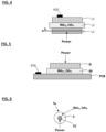
- Figure 4 schematically illustrates a model for the shunt EC2 including a copper outer layer L1, where the temperature is detected with the sensor 410, a copper inner layer L3, through which a current I 2 flows, and an insulation layer L2, called "pre-preg", interposed between the outer layer L1 and the inner layer L3.
- the iterative process includes the following steps S1_EC2 and S2_EC2 executed for the shunt EC2.
- the processing module 230 acquires the following values:
- the processing module 230 processes the input data using the thermal model.
- the processing includes the steps S20_EC2 to S27_EC2 described below.
- the value of the electrical resistance of the shunt EC2 may be set to the reference resistance value R ref, 2 of the shunt EC2 at room temperature.
- the processing module 230 determines a value dT 2 ,i of temperature difference of the shunt EC2 relative to the ambient temperature Ta. For that purpose, the processing module 230 computes the cumulated temperature variation between the initial time t 0 and the current time t i , by adding ⁇ T 2 ,i to the value of temperature difference dT 2 ,i- 1 of the shunt EC2 relative to the ambient temperature Ta determined at the previous iteration of time t i-1 , based on the equation (5).
- the current flowing through the shunt EC2 may be averaged every N iterations of the process.
- the current I 2 ( t i ) can be summed up until the N iterations of the step S25_EC2 have been executed during each cycle of N consecutive iterations.
- the sum of the N successive current values I 2 ( t i ) is then divided by N to determine the average current I 2 ⁇ .
- a step S3 of monitoring the output of the processing step S2 may be performed for the shunt EC2.
- the diagnostic module 240 may compare the temperature difference dT 2 ,i , and/or the temperature T 2 ( t i ), and/or the current I 2 ( t i ), and/or the averaged current I 2 ⁇ t i , to respective thresholds, so as to detect an abnormality in the system 100.
- the transistor EC1 may be turned off and/or an alert may be triggered.
- the diagnostic module 240 may include an analog comparator 242 configured to quickly detect that the current I 2 flowing through the shunt EC2 exceeds a maximal value of current, prestored in the non-volatile memory of the memory system 220, and denoted as Ids max .
- the maximal current Ids max may be the maximal drain-source current allowed through the transistor EC1.
- the analog comparator may be a voltage comparator configured to receive in input a maximal analog voltage V 2 max ( t i ) through the shunt EC2 and the measured voltage through the shunt EC2, at each time t i .
- the output of the comparator 242 is connected to the controlling module 250.
- the comparator 242 transmits to the controlling module 250 a signal indicative of a peak of current that is too high.
- the controlling module 250 upon receiving this signal, the controlling module 250 turns off the transistor EC1.
- the transistor EC1 is mounted on the printed circuit board 400.
- the transistor EC1 is a device used to switch on or off the load 300.
- Figure 5 schematically illustrates a model for the transistor EC1 including: a first layer D representing a die or semiconductor part of the transistor EC1, that receives the electrical power P 1 , a second layer M representing a metal material conducting heat, a third layer PCB representing the printed circuit board 400, where the ambient temperature is detected with the sensor 410.
- the transistor EC1 is a MOSFET.
- the MOSFET has three terminals: drain, gate and source.
- the processing module 230 acquires the following values:
- the current I 2 through the shunt EC2 corresponds to the drain source current I ds (t i ) flowing through the transistor EC1.
- I 2 t i I ds t i
- I 2 ⁇ t i I ds ⁇ t i
- the processing module 230 processes the input data using the thermal model.
- the processing includes the steps S20_EC1 to S27_EC1 described below.
- the processing module 230 may estimate a value dT 1 ,i of temperature difference of the transistor EC1 relative to the ambient temperature Ta. For that purpose, the processing module 230 may compute the cumulated temperature variation between the initial time t 0 and the current time t i , by adding ⁇ T 1 ,i to the value of temperature difference dT 1 ,i- 1 of the transistor EC1 relative to the ambient temperature Ta determined at the previous iteration of time t i-1 , based on the equation (5).
- a monitoring step S3_EC1 may then be performed to monitor the reliability of the transistor EC1 based on the output of the processing step S2.
- the diagnostic module 240 may perform at least one of the following monitoring actions :
- the diagnostic module 240 If the temperature T 1 ( t i ) of the transistor EC1 is above T 1 max , or the temperature difference dT 1 ,i is above dT 1 max , or the transistor resistance value R ds ( t i ) is above R dsmax , the diagnostic module 240 generates control signal for turning off the transistor EC1 and/or generating an alert signal.
- the temperature of the transistor EC1 can be monitored, and if it is too high, the transistor EC1 may be turned off.
- the transient temperature that is the difference or variation between the die temperature of the transistor EC1 and the temperature measured on the printed circuit board PCB 400, can also be monitored. If the transient temperature is too high, the transistor EC1 may also be turned off. Indeed, an important transient temperature is likely to produce stress on the transistor EC1.
- the drain source resistance R ds of the transistor EC1 can also be monitored, when the transistor EC1 is fully conducting. If the resistance R ds is too high, the transistor EC1 may be turned off too.
- the diagnostic module 240 generates an alert signal warning that the transistor EC1 may have an abnormality and may not be reliable.
- the cable EC3 connects the shunt EC2 on the printed circuit board 400 and the load 300 that is external to the printed circuit board 400.
- the cable EC3 is external to the printed circuit board 400.
- Figure 6 schematically illustrates an example of model for the cable EC3: it includes a core cable CC in copper surrounded by an insulation layer or sleeve S.
- the core cable CC is provided with a certain electrical power and, due to power loss, heat is transferred from the core cable CC to the external surface of the cable EC2 where the temperature is equal to an ambient temperature Ta in the external environment surrounding the cable EC3.
- the ambient temperature Ta around the cable EC3 is not measured.
- the ambient temperature Ta is assumed to be equal to a maximal ambience temperature Ta_max that is expected in the environment surrounding the cable EC3.
- a maximal temperature in the vehicle can be predetermined.
- the processing module 230 acquires the following values:
- the current I 2 through the shunt EC2 corresponds to the current flowing through the cable EC3.
- the processing module 230 processes the input data using the thermal model.
- the processing includes the steps S20_EC3 to S27_EC3 described below.
- the value of the electrical resistance of the cable EC3 may be set to the reference resistance value R ref, 3 of the cable EC3 at room temperature.
- the processing module 230 may estimate a value dT 3 ,i of temperature difference of the cable EC3 relative to the ambient temperature Ta between the initial time t 0 and the current time t i .
- the processing module 230 may compute the cumulated temperature variation by adding ⁇ T 3 ,i to the value of the temperature difference dT 3 ,i- 1 of the cable EC3 relative to the ambient temperature Ta determined at the previous iteration of time t i-1 , based on the equation (5).
- a step S3_EC3 of monitoring the reliability of the cable EC3 based on the output of the processing step S2_EC3 may be performed for the cable EC3.
- the diagnostic module 240 may compare the temperature difference dT 3 ,i to a predetermined maximal temperature increase of the cable EC3, so as to detect an abnormality in the system 100.
- the monitoring device 200 and the system 100 can be included in a vehicle.
- the present disclosure also concerns a computer program comprising instructions which, when the program is executed by a processor, cause the processor to carry out the steps of the method previously described.
- the present method can be implemented only with hardware.
- the present disclosure also concerns a monitoring device configured to monitor reliability of the electrical components of the system 100, comprising only hardware means adapted to perform the steps of the method previously defined.
- the monitoring device may be for example by a digital state machine.
Landscapes
- Physics & Mathematics (AREA)
- General Physics & Mathematics (AREA)
- Engineering & Computer Science (AREA)
- Microelectronics & Electronic Packaging (AREA)
- Environmental & Geological Engineering (AREA)
- Testing Of Individual Semiconductor Devices (AREA)
Claims (13)
- Procédé de surveillance de la fiabilité d'un système (100) comportant une pluralité de composants électriques (EC1, EC2,...), comprenant les étapes, effectuées pour chacun de la pluralité de composants électriques (EC1, EC2,...), de réception (S1) des données d'entrée comportant une tension aux bornes du composant électrique et/ou un courant à travers le composant électrique et/ou une valeur de résistance électrique du composant électrique.le traitement (S2) des données d'entrée à l'aide d'un modèle thermique mémorisé représentant le transfert de chaleur dudit composant électrique, le transfert de chaleur se rapportant au flux de chaleur entre un premier point du composant électrique, où la température doit être estimée, et un second point à une température de référence connue (Ta), pour déterminer une différence de température dudit composant électrique par rapport à la température de référence (Ta) ;dans lequell'étape de traitement (S2_EC2) est d'abord effectuée pour un premier composant électrique (EC2) de la pluralité de composants électriques (EC1, EC2,...) et comporte en outre l'estimation d'une valeur du courant électrique en fonction de ladite différence de température déterminée dudit premier composant électrique (EC2), puis l'étape de traitement (S2_EC1) est effectuée pour un second composant électrique (EC1) de la pluralité de composants électriques (EC1, EC2,...) à l'aide de la valeur de courant électrique estimée comme données d'entrée ;
etla surveillance (S3) de la fiabilité du système (100) en fonction des données de sortie des étapes de traitement (S2_EC2, S2_EC1). - Procédé selon la revendication 1, dans lequel l'étape de traitement des données d'entrée comporte une étape d'estimation d'une puissance électrique (Pn(ti)) dissipée par ledit au moins un composant électrique (ECn).
- Procédé selon l'une quelconque des revendications 1 à 2, dans lequelles étapes (S1, S2) de réception et de traitement des données d'entrée sont effectuées de manière itérative pour déterminer (S21), à chaque itération, une valeur d'une variation incrémentale de la température du composant électrique (ECn) par rapport à la température de référence, sur une étape temporelle,et l'étape de traitement (S2) comporte en outre l'accumulation (S22) des valeurs successives de la variation incrémentale de la température afin d'estimer une valeur de différence de température du composant électrique (ECn) par rapport à la température de référence.
- Procédé selon la revendication 3, comportant en outre une étape (S24) consistant à estimer, à chaque itération, une valeur de résistance électrique du composant électrique (ECn) en fonction de la température de référence et de la valeur déterminée de la différence de température du composant électrique par rapport à la température de référence.
- Procédé selon la revendication 4, dans lequel la valeur estimée de la résistance électrique du composant électrique (ECn) est utilisée comme donnée d'entrée à l'itération suivante dans l'étape (S2) de traitement des données d'entrée pour déterminer les informations de température du composant électrique (ECn).
- Procédé selon la revendication 4 ou 5, dans lequel l'étape de traitement (S2) comporte en outre une étape (S25) consistant à estimer, à chaque itération, une valeur de courant électrique circulant à travers le composant électrique (ECn) à partir d'une valeur de tension mesurée aux bornes du composant électrique (ECn) et de la valeur de résistance électrique déterminée du composant électrique (ECn).
- Procédé selon l'une quelconque des revendications 1 à 6, dans lequel la pluralité de composants électriques comporte un composant électrique (EC1, EC2) monté sur une carte de circuits imprimés, PCB, (400) et
l'étape (S1) de réception des données d'entrée comporte en outre la réception d'une température mesurée provenant d'un capteur monté sur la carte de circuits imprimés (400), afin d'obtenir la température de référence. - Procédé selon l'une quelconque des revendications 1 à 7, dans lequel l'étape (S1) de réception des données d'entrée comporte en outre la récupération à partir de la mémoire d'une température ambiante maximale prémémorisée qui est attendue à proximité du composant électrique (EC3), pour obtenir la température de référence.
- Procédé selon l'une quelconque des revendications 1 à 8, comportant en outre une étape (S3) de comparaison des données de sortie provenant de l'étape de traitement (S2) effectuée pour ledit au moins un composant électrique (ECn) avec une valeur de seuil pour détecter une anomalie dans le système (100) et une étape (S4) de mise hors tension du système ou de déclenchement d'une alerte lorsqu'une anomalie dans le système (100) est détectée.
- Programme informatique comprenant des instructions qui, lorsque le programme est exécuté par un processeur, amènent le processeur à mettre en œuvre les étapes du procédé selon l'une quelconque des revendications 1 à 9.
- Dispositif de surveillance (200) conçu pour surveiller la fiabilité d'un système comportant une pluralité de composants électriques, comprenant une mémoire mémorisant des caractéristiques thermiques prédéfinies d'un modèle thermique représentant le transfert de chaleur pour chacun de la pluralité de composants électriques dudit système, le transfert de chaleur se rapportant au flux de chaleur entre un premier point du composant électrique, où la température doit être estimée, et un second point présentant une température de référence connue (Ta) ;
un processeur apte à effectuer les étapes du procédé selon l'une quelconque des revendications 1 à 9. - Dispositif de surveillance conçu pour surveiller la fiabilité d'un système comportant une pluralité de composants électriques, comprenant uniquement un moyen matériel apte à effectuer les étapes du procédé selon l'une quelconque des revendications 1 à 9.
- Véhicule comportant le dispositif de surveillance selon l'une quelconque des revendications 11 à 12.
Priority Applications (3)
| Application Number | Priority Date | Filing Date | Title |
|---|---|---|---|
| EP22203094.2A EP4357743B1 (fr) | 2022-10-21 | 2022-10-21 | Procédé de surveillance de la fiabilité d'un système comprenant des composants électriques |
| CN202311360129.9A CN118549723A (zh) | 2022-10-21 | 2023-10-19 | 监测包括电气部件的系统的可靠性的方法 |
| US18/491,766 US12560641B2 (en) | 2022-10-21 | 2023-10-21 | Method of monitoring reliability of system including electrical components |
Applications Claiming Priority (1)
| Application Number | Priority Date | Filing Date | Title |
|---|---|---|---|
| EP22203094.2A EP4357743B1 (fr) | 2022-10-21 | 2022-10-21 | Procédé de surveillance de la fiabilité d'un système comprenant des composants électriques |
Publications (2)
| Publication Number | Publication Date |
|---|---|
| EP4357743A1 EP4357743A1 (fr) | 2024-04-24 |
| EP4357743B1 true EP4357743B1 (fr) | 2025-06-25 |
Family
ID=83994916
Family Applications (1)
| Application Number | Title | Priority Date | Filing Date |
|---|---|---|---|
| EP22203094.2A Active EP4357743B1 (fr) | 2022-10-21 | 2022-10-21 | Procédé de surveillance de la fiabilité d'un système comprenant des composants électriques |
Country Status (3)
| Country | Link |
|---|---|
| US (1) | US12560641B2 (fr) |
| EP (1) | EP4357743B1 (fr) |
| CN (1) | CN118549723A (fr) |
Family Cites Families (24)
| Publication number | Priority date | Publication date | Assignee | Title |
|---|---|---|---|---|
| US6092927A (en) * | 1994-11-10 | 2000-07-25 | International Rectifier Corp. | Temperature detection of power semiconductors performed by a co-packaged analog integrated circuit |
| EP0749208A2 (fr) | 1995-06-15 | 1996-12-18 | AT&T IPM Corp. | Circuit de protection pour transistor à effet de champ |
| US6891739B2 (en) | 2002-03-04 | 2005-05-10 | International Rectifier Corporation | H-bridge with power switches and control in a single package |
| JP2005039152A (ja) | 2003-07-18 | 2005-02-10 | Shinko Electric Ind Co Ltd | 半導体装置の製造方法 |
| CN100420139C (zh) | 2003-09-19 | 2008-09-17 | 株式会社三社电机制作所 | 电镀电源装置 |
| US7839201B2 (en) | 2005-04-01 | 2010-11-23 | Raytheon Company | Integrated smart power switch |
| US7826985B2 (en) * | 2008-05-02 | 2010-11-02 | Rockwell Automation Technologies, Inc. | Power module life estimation fatigue function |
| US7940034B2 (en) | 2008-05-19 | 2011-05-10 | Infineon Technologies Austria Ag | Apparatus for detecting a state of operation of a power semiconductor device |
| DE102008027428B4 (de) | 2008-06-09 | 2021-08-12 | Texas Instruments Deutschland Gmbh | Integrierte Batterieladegerät-Schutzschaltung |
| CN101777501B (zh) | 2009-01-09 | 2012-04-25 | 致伸科技股份有限公司 | 影像撷取装置的组装方法以及感光芯片的封装方法 |
| CN102449524B (zh) | 2009-03-25 | 2015-03-11 | 马格纳电子系统公司 | 车辆摄相机和透镜组装 |
| EP3054306A1 (fr) * | 2015-02-03 | 2016-08-10 | Siemens Aktiengesellschaft | Procédé de détermination d'un vieillissement de modules semi-conducteurs de puissance, dispositif et circuit |
| JP6837842B2 (ja) | 2017-01-11 | 2021-03-03 | 矢崎総業株式会社 | 半導体スイッチ制御装置 |
| CN111727463B (zh) | 2018-01-19 | 2025-04-11 | 松下电器(美国)知识产权公司 | 三维数据编码方法、三维数据解码方法、三维数据编码装置、以及三维数据解码装置 |
| EP3745355A4 (fr) | 2018-01-26 | 2021-03-24 | Panasonic Intellectual Property Corporation of America | Procédé de codage de données tridimensionnelles, procédé de décodage de données tridimensionnelles, dispositif de codage de données tridimensionnelles et dispositif de décodage de données tridimensionnelles |
| US10955297B2 (en) | 2018-06-07 | 2021-03-23 | General Electric Company | Systems and methods for monitoring junction temperature of a semiconductor switch |
| DE102018212870A1 (de) * | 2018-08-02 | 2020-02-06 | Volkswagen Aktiengesellschaft | Verfahren und Vorrichtung zum Schätzen der Temperatur eines Halbleiterbauelementes sowie Computerprogramm |
| CN111339623B (zh) * | 2018-11-30 | 2022-09-23 | 中车时代电动汽车股份有限公司 | 一种功率模块温度估算方法 |
| CN111323993A (zh) | 2018-12-15 | 2020-06-23 | 三赢科技(深圳)有限公司 | 镜头模组及电子装置 |
| US11368150B2 (en) | 2019-01-17 | 2022-06-21 | Texas Instruments Incorporated | Reliabtility monitor for field effect transistor devices |
| EP3855624A1 (fr) | 2020-01-22 | 2021-07-28 | Infineon Technologies AG | Circuit et dispositif de protection de surtension |
| CN111783287B (zh) * | 2020-06-19 | 2022-10-04 | 合肥工业大学 | 三相igbt功率模块的在线结温计算方法 |
| US20220018720A1 (en) * | 2020-07-20 | 2022-01-20 | Dana Tm4 Inc. | Sensing junction temperature of power transistors |
| US11378614B2 (en) | 2020-09-01 | 2022-07-05 | Infineon Technologies Ag | Temperature detection of power switch using modulation of driver output impedance |
-
2022
- 2022-10-21 EP EP22203094.2A patent/EP4357743B1/fr active Active
-
2023
- 2023-10-19 CN CN202311360129.9A patent/CN118549723A/zh active Pending
- 2023-10-21 US US18/491,766 patent/US12560641B2/en active Active
Also Published As
| Publication number | Publication date |
|---|---|
| CN118549723A (zh) | 2024-08-27 |
| US12560641B2 (en) | 2026-02-24 |
| US20240151765A1 (en) | 2024-05-09 |
| EP4357743A1 (fr) | 2024-04-24 |
Similar Documents
| Publication | Publication Date | Title |
|---|---|---|
| US8767367B2 (en) | Wire protection method and wire protection device | |
| JP5448706B2 (ja) | 電流検出装置及び電流検出方法 | |
| JP4807352B2 (ja) | 温度検出システム | |
| JP6490096B2 (ja) | 温度補償付シャント電流測定 | |
| US9129510B2 (en) | Monitoring operating condition of electrical component | |
| EP3159992B1 (fr) | Dispositif de commande d'un fusible électronique et procédé de commande d'un fusible électronique | |
| EP3531146B1 (fr) | Surveillance de module à semi-conducteur de puissance à connexion par fils | |
| JP2002318162A (ja) | 異常の検知方法および保護装置、並びに、温度の推定方法および推定装置 | |
| WO1996011390A1 (fr) | Detecteur transmetteur | |
| CN207456645U (zh) | 温度变送器和温度变送器组件 | |
| CN1965241B (zh) | 老化装置的状态诊断方法 | |
| JP6864069B2 (ja) | 自己発熱を補償することによる正確なバッテリ温度測定 | |
| US12055583B2 (en) | Method and device for estimating the ageing of an electronic component | |
| US10036670B2 (en) | Systems and methods for peak junction temperature sensing and thermal safe operating area protection | |
| EP4357743A1 (fr) | Procédé de surveillance de la fiabilité d'un système comprenant des composants électriques | |
| US6983223B2 (en) | Detecting thermocouple failure using loop resistance | |
| JP2009226984A (ja) | 電線保護方法および電線保護装置 | |
| US10634565B2 (en) | Temperature sensing apparatus and temperature sensing method thereof | |
| KR20140014629A (ko) | 전동식 파워 스티어링 제어 온도값 산출 장치 및 방법과 이를 이용한 전동식 파워 스티어링 제어 시스템 | |
| CN111044913B (zh) | 用于运行电池传感器的方法和电池传感器 | |
| EP2821799B1 (fr) | Mesure de courant extrêmement précise | |
| JPH0476799A (ja) | 熱電対温度センサの寿命判定及び寿命予測装置 | |
| CN116147805A (zh) | 一种用于泵站填料函温度监测的冗余监测方法和系统 | |
| JP3116882B2 (ja) | 微少過負荷電流監視回路 | |
| US20250347723A1 (en) | Distributed dynamic temperature compensation for shunts |
Legal Events
| Date | Code | Title | Description |
|---|---|---|---|
| PUAI | Public reference made under article 153(3) epc to a published international application that has entered the european phase |
Free format text: ORIGINAL CODE: 0009012 |
|
| STAA | Information on the status of an ep patent application or granted ep patent |
Free format text: STATUS: THE APPLICATION HAS BEEN PUBLISHED |
|
| AK | Designated contracting states |
Kind code of ref document: A1 Designated state(s): AL AT BE BG CH CY CZ DE DK EE ES FI FR GB GR HR HU IE IS IT LI LT LU LV MC ME MK MT NL NO PL PT RO RS SE SI SK SM TR |
|
| RAP3 | Party data changed (applicant data changed or rights of an application transferred) |
Owner name: APTIV TECHNOLOGIES AG |
|
| STAA | Information on the status of an ep patent application or granted ep patent |
Free format text: STATUS: REQUEST FOR EXAMINATION WAS MADE |
|
| 17P | Request for examination filed |
Effective date: 20240923 |
|
| RBV | Designated contracting states (corrected) |
Designated state(s): AL AT BE BG CH CY CZ DE DK EE ES FI FR GB GR HR HU IE IS IT LI LT LU LV MC ME MK MT NL NO PL PT RO RS SE SI SK SM TR |
|
| GRAP | Despatch of communication of intention to grant a patent |
Free format text: ORIGINAL CODE: EPIDOSNIGR1 |
|
| STAA | Information on the status of an ep patent application or granted ep patent |
Free format text: STATUS: GRANT OF PATENT IS INTENDED |
|
| RIC1 | Information provided on ipc code assigned before grant |
Ipc: G01K 3/00 20060101ALI20241220BHEP Ipc: G01K 7/42 20060101AFI20241220BHEP |
|
| INTG | Intention to grant announced |
Effective date: 20250122 |
|
| GRAS | Grant fee paid |
Free format text: ORIGINAL CODE: EPIDOSNIGR3 |
|
| GRAA | (expected) grant |
Free format text: ORIGINAL CODE: 0009210 |
|
| STAA | Information on the status of an ep patent application or granted ep patent |
Free format text: STATUS: THE PATENT HAS BEEN GRANTED |
|
| AK | Designated contracting states |
Kind code of ref document: B1 Designated state(s): AL AT BE BG CH CY CZ DE DK EE ES FI FR GB GR HR HU IE IS IT LI LT LU LV MC ME MK MT NL NO PL PT RO RS SE SI SK SM TR |
|
| REG | Reference to a national code |
Ref country code: GB Ref legal event code: FG4D |
|
| REG | Reference to a national code |
Ref country code: CH Ref legal event code: EP |
|
| REG | Reference to a national code |
Ref country code: DE Ref legal event code: R096 Ref document number: 602022016381 Country of ref document: DE |
|
| REG | Reference to a national code |
Ref country code: CH Ref legal event code: EP |
|
| P01 | Opt-out of the competence of the unified patent court (upc) registered |
Free format text: CASE NUMBER: APP_27281/2025 Effective date: 20250609 |
|
| REG | Reference to a national code |
Ref country code: IE Ref legal event code: FG4D |
|
| PG25 | Lapsed in a contracting state [announced via postgrant information from national office to epo] |
Ref country code: FI Free format text: LAPSE BECAUSE OF FAILURE TO SUBMIT A TRANSLATION OF THE DESCRIPTION OR TO PAY THE FEE WITHIN THE PRESCRIBED TIME-LIMIT Effective date: 20250625 |
|
| REG | Reference to a national code |
Ref country code: LT Ref legal event code: MG9D |
|
| PG25 | Lapsed in a contracting state [announced via postgrant information from national office to epo] |
Ref country code: NO Free format text: LAPSE BECAUSE OF FAILURE TO SUBMIT A TRANSLATION OF THE DESCRIPTION OR TO PAY THE FEE WITHIN THE PRESCRIBED TIME-LIMIT Effective date: 20250925 Ref country code: GR Free format text: LAPSE BECAUSE OF FAILURE TO SUBMIT A TRANSLATION OF THE DESCRIPTION OR TO PAY THE FEE WITHIN THE PRESCRIBED TIME-LIMIT Effective date: 20250926 |
|
| PG25 | Lapsed in a contracting state [announced via postgrant information from national office to epo] |
Ref country code: BG Free format text: LAPSE BECAUSE OF FAILURE TO SUBMIT A TRANSLATION OF THE DESCRIPTION OR TO PAY THE FEE WITHIN THE PRESCRIBED TIME-LIMIT Effective date: 20250625 |
|
| PG25 | Lapsed in a contracting state [announced via postgrant information from national office to epo] |
Ref country code: HR Free format text: LAPSE BECAUSE OF FAILURE TO SUBMIT A TRANSLATION OF THE DESCRIPTION OR TO PAY THE FEE WITHIN THE PRESCRIBED TIME-LIMIT Effective date: 20250625 |
|
| PG25 | Lapsed in a contracting state [announced via postgrant information from national office to epo] |
Ref country code: RS Free format text: LAPSE BECAUSE OF FAILURE TO SUBMIT A TRANSLATION OF THE DESCRIPTION OR TO PAY THE FEE WITHIN THE PRESCRIBED TIME-LIMIT Effective date: 20250925 |
|
| PG25 | Lapsed in a contracting state [announced via postgrant information from national office to epo] |
Ref country code: LV Free format text: LAPSE BECAUSE OF FAILURE TO SUBMIT A TRANSLATION OF THE DESCRIPTION OR TO PAY THE FEE WITHIN THE PRESCRIBED TIME-LIMIT Effective date: 20250625 |
|
| REG | Reference to a national code |
Ref country code: NL Ref legal event code: MP Effective date: 20250625 |
|
| PG25 | Lapsed in a contracting state [announced via postgrant information from national office to epo] |
Ref country code: NL Free format text: LAPSE BECAUSE OF FAILURE TO SUBMIT A TRANSLATION OF THE DESCRIPTION OR TO PAY THE FEE WITHIN THE PRESCRIBED TIME-LIMIT Effective date: 20250625 |
|
| PG25 | Lapsed in a contracting state [announced via postgrant information from national office to epo] |
Ref country code: PT Free format text: LAPSE BECAUSE OF FAILURE TO SUBMIT A TRANSLATION OF THE DESCRIPTION OR TO PAY THE FEE WITHIN THE PRESCRIBED TIME-LIMIT Effective date: 20251027 |
|
| REG | Reference to a national code |
Ref country code: AT Ref legal event code: MK05 Ref document number: 1806877 Country of ref document: AT Kind code of ref document: T Effective date: 20250625 |
|
| PG25 | Lapsed in a contracting state [announced via postgrant information from national office to epo] |
Ref country code: IS Free format text: LAPSE BECAUSE OF FAILURE TO SUBMIT A TRANSLATION OF THE DESCRIPTION OR TO PAY THE FEE WITHIN THE PRESCRIBED TIME-LIMIT Effective date: 20251025 |
|
| PGFP | Annual fee paid to national office [announced via postgrant information from national office to epo] |
Ref country code: DE Payment date: 20250917 Year of fee payment: 4 |
|
| PG25 | Lapsed in a contracting state [announced via postgrant information from national office to epo] |
Ref country code: AT Free format text: LAPSE BECAUSE OF FAILURE TO SUBMIT A TRANSLATION OF THE DESCRIPTION OR TO PAY THE FEE WITHIN THE PRESCRIBED TIME-LIMIT Effective date: 20250625 Ref country code: SM Free format text: LAPSE BECAUSE OF FAILURE TO SUBMIT A TRANSLATION OF THE DESCRIPTION OR TO PAY THE FEE WITHIN THE PRESCRIBED TIME-LIMIT Effective date: 20250625 |
|
| PGFP | Annual fee paid to national office [announced via postgrant information from national office to epo] |
Ref country code: FR Payment date: 20251014 Year of fee payment: 4 |
|
| PG25 | Lapsed in a contracting state [announced via postgrant information from national office to epo] |
Ref country code: CZ Free format text: LAPSE BECAUSE OF FAILURE TO SUBMIT A TRANSLATION OF THE DESCRIPTION OR TO PAY THE FEE WITHIN THE PRESCRIBED TIME-LIMIT Effective date: 20250625 |
|
| PG25 | Lapsed in a contracting state [announced via postgrant information from national office to epo] |
Ref country code: PL Free format text: LAPSE BECAUSE OF FAILURE TO SUBMIT A TRANSLATION OF THE DESCRIPTION OR TO PAY THE FEE WITHIN THE PRESCRIBED TIME-LIMIT Effective date: 20250625 |
|
| PG25 | Lapsed in a contracting state [announced via postgrant information from national office to epo] |
Ref country code: EE Free format text: LAPSE BECAUSE OF FAILURE TO SUBMIT A TRANSLATION OF THE DESCRIPTION OR TO PAY THE FEE WITHIN THE PRESCRIBED TIME-LIMIT Effective date: 20250625 |
|
| PG25 | Lapsed in a contracting state [announced via postgrant information from national office to epo] |
Ref country code: SK Free format text: LAPSE BECAUSE OF FAILURE TO SUBMIT A TRANSLATION OF THE DESCRIPTION OR TO PAY THE FEE WITHIN THE PRESCRIBED TIME-LIMIT Effective date: 20250625 |
|
| PG25 | Lapsed in a contracting state [announced via postgrant information from national office to epo] |
Ref country code: ES Free format text: LAPSE BECAUSE OF FAILURE TO SUBMIT A TRANSLATION OF THE DESCRIPTION OR TO PAY THE FEE WITHIN THE PRESCRIBED TIME-LIMIT Effective date: 20250625 |
|
| PG25 | Lapsed in a contracting state [announced via postgrant information from national office to epo] |
Ref country code: RO Free format text: LAPSE BECAUSE OF FAILURE TO SUBMIT A TRANSLATION OF THE DESCRIPTION OR TO PAY THE FEE WITHIN THE PRESCRIBED TIME-LIMIT Effective date: 20250625 |
|
| REG | Reference to a national code |
Ref country code: DE Ref legal event code: R097 Ref document number: 602022016381 Country of ref document: DE |
|
| PG25 | Lapsed in a contracting state [announced via postgrant information from national office to epo] |
Ref country code: DK Free format text: LAPSE BECAUSE OF FAILURE TO SUBMIT A TRANSLATION OF THE DESCRIPTION OR TO PAY THE FEE WITHIN THE PRESCRIBED TIME-LIMIT Effective date: 20250625 |
|
| PG25 | Lapsed in a contracting state [announced via postgrant information from national office to epo] |
Ref country code: IT Free format text: LAPSE BECAUSE OF FAILURE TO SUBMIT A TRANSLATION OF THE DESCRIPTION OR TO PAY THE FEE WITHIN THE PRESCRIBED TIME-LIMIT Effective date: 20250625 |
|
| PLBE | No opposition filed within time limit |
Free format text: ORIGINAL CODE: 0009261 |
|
| STAA | Information on the status of an ep patent application or granted ep patent |
Free format text: STATUS: NO OPPOSITION FILED WITHIN TIME LIMIT |
|
| REG | Reference to a national code |
Ref country code: CH Ref legal event code: L10 Free format text: ST27 STATUS EVENT CODE: U-0-0-L10-L00 (AS PROVIDED BY THE NATIONAL OFFICE) Effective date: 20260507 |
|
| REG | Reference to a national code |
Ref country code: CH Ref legal event code: H13 Free format text: ST27 STATUS EVENT CODE: U-0-0-H10-H13 (AS PROVIDED BY THE NATIONAL OFFICE) Effective date: 20260527 |
|
| 26N | No opposition filed |
Effective date: 20260326 |
|
| PG25 | Lapsed in a contracting state [announced via postgrant information from national office to epo] |
Ref country code: LU Free format text: LAPSE BECAUSE OF NON-PAYMENT OF DUE FEES Effective date: 20251021 |
|
| REG | Reference to a national code |
Ref country code: BE Ref legal event code: MM Effective date: 20251031 |
|
| PG25 | Lapsed in a contracting state [announced via postgrant information from national office to epo] |
Ref country code: LT Free format text: LAPSE BECAUSE OF FAILURE TO SUBMIT A TRANSLATION OF THE DESCRIPTION OR TO PAY THE FEE WITHIN THE PRESCRIBED TIME-LIMIT Effective date: 20250625 |
|
| PG25 | Lapsed in a contracting state [announced via postgrant information from national office to epo] |
Ref country code: MC Free format text: LAPSE BECAUSE OF FAILURE TO SUBMIT A TRANSLATION OF THE DESCRIPTION OR TO PAY THE FEE WITHIN THE PRESCRIBED TIME-LIMIT Effective date: 20250625 |
|
| PG25 | Lapsed in a contracting state [announced via postgrant information from national office to epo] |
Ref country code: BE Free format text: LAPSE BECAUSE OF NON-PAYMENT OF DUE FEES Effective date: 20251031 Ref country code: CH Free format text: LAPSE BECAUSE OF NON-PAYMENT OF DUE FEES Effective date: 20251031 |
|
| PG25 | Lapsed in a contracting state [announced via postgrant information from national office to epo] |
Ref country code: SE Free format text: LAPSE BECAUSE OF FAILURE TO SUBMIT A TRANSLATION OF THE DESCRIPTION OR TO PAY THE FEE WITHIN THE PRESCRIBED TIME-LIMIT Effective date: 20250625 |