EP4366149A1 - Dispositif de conversion de puissance - Google Patents
Dispositif de conversion de puissance Download PDFInfo
- Publication number
- EP4366149A1 EP4366149A1 EP21948331.0A EP21948331A EP4366149A1 EP 4366149 A1 EP4366149 A1 EP 4366149A1 EP 21948331 A EP21948331 A EP 21948331A EP 4366149 A1 EP4366149 A1 EP 4366149A1
- Authority
- EP
- European Patent Office
- Prior art keywords
- manipulated variable
- frequency
- phase shift
- shift amount
- function
- Prior art date
- Legal status (The legal status is an assumption and is not a legal conclusion. Google has not performed a legal analysis and makes no representation as to the accuracy of the status listed.)
- Withdrawn
Links
Images








Classifications
-
- H—ELECTRICITY
- H02—GENERATION; CONVERSION OR DISTRIBUTION OF ELECTRIC POWER
- H02M—APPARATUS FOR CONVERSION BETWEEN AC AND AC, BETWEEN AC AND DC, OR BETWEEN DC AND DC, AND FOR USE WITH MAINS OR SIMILAR POWER SUPPLY SYSTEMS; CONVERSION OF DC OR AC INPUT POWER INTO SURGE OUTPUT POWER; CONTROL OR REGULATION THEREOF
- H02M3/00—Conversion of DC power input into DC power output
- H02M3/22—Conversion of DC power input into DC power output with intermediate conversion into AC
- H02M3/24—Conversion of DC power input into DC power output with intermediate conversion into AC by static converters
- H02M3/28—Conversion of DC power input into DC power output with intermediate conversion into AC by static converters using discharge tubes with control electrode or semiconductor devices with control electrode to produce the intermediate AC
- H02M3/325—Conversion of DC power input into DC power output with intermediate conversion into AC by static converters using discharge tubes with control electrode or semiconductor devices with control electrode to produce the intermediate AC using devices of a triode or a transistor type requiring continuous application of a control signal
- H02M3/335—Conversion of DC power input into DC power output with intermediate conversion into AC by static converters using discharge tubes with control electrode or semiconductor devices with control electrode to produce the intermediate AC using devices of a triode or a transistor type requiring continuous application of a control signal using semiconductor devices only
- H02M3/33569—Conversion of DC power input into DC power output with intermediate conversion into AC by static converters using discharge tubes with control electrode or semiconductor devices with control electrode to produce the intermediate AC using devices of a triode or a transistor type requiring continuous application of a control signal using semiconductor devices only having several active switching elements
-
- H—ELECTRICITY
- H02—GENERATION; CONVERSION OR DISTRIBUTION OF ELECTRIC POWER
- H02M—APPARATUS FOR CONVERSION BETWEEN AC AND AC, BETWEEN AC AND DC, OR BETWEEN DC AND DC, AND FOR USE WITH MAINS OR SIMILAR POWER SUPPLY SYSTEMS; CONVERSION OF DC OR AC INPUT POWER INTO SURGE OUTPUT POWER; CONTROL OR REGULATION THEREOF
- H02M1/00—Details of apparatus for conversion
- H02M1/0003—Details of control, feedback or regulation circuits
- H02M1/0012—Control circuits using digital or numerical techniques
-
- H—ELECTRICITY
- H02—GENERATION; CONVERSION OR DISTRIBUTION OF ELECTRIC POWER
- H02M—APPARATUS FOR CONVERSION BETWEEN AC AND AC, BETWEEN AC AND DC, OR BETWEEN DC AND DC, AND FOR USE WITH MAINS OR SIMILAR POWER SUPPLY SYSTEMS; CONVERSION OF DC OR AC INPUT POWER INTO SURGE OUTPUT POWER; CONTROL OR REGULATION THEREOF
- H02M3/00—Conversion of DC power input into DC power output
- H02M3/01—Resonant DC/DC converters
-
- H—ELECTRICITY
- H02—GENERATION; CONVERSION OR DISTRIBUTION OF ELECTRIC POWER
- H02M—APPARATUS FOR CONVERSION BETWEEN AC AND AC, BETWEEN AC AND DC, OR BETWEEN DC AND DC, AND FOR USE WITH MAINS OR SIMILAR POWER SUPPLY SYSTEMS; CONVERSION OF DC OR AC INPUT POWER INTO SURGE OUTPUT POWER; CONTROL OR REGULATION THEREOF
- H02M3/00—Conversion of DC power input into DC power output
- H02M3/22—Conversion of DC power input into DC power output with intermediate conversion into AC
- H02M3/24—Conversion of DC power input into DC power output with intermediate conversion into AC by static converters
- H02M3/28—Conversion of DC power input into DC power output with intermediate conversion into AC by static converters using discharge tubes with control electrode or semiconductor devices with control electrode to produce the intermediate AC
- H02M3/325—Conversion of DC power input into DC power output with intermediate conversion into AC by static converters using discharge tubes with control electrode or semiconductor devices with control electrode to produce the intermediate AC using devices of a triode or a transistor type requiring continuous application of a control signal
- H02M3/335—Conversion of DC power input into DC power output with intermediate conversion into AC by static converters using discharge tubes with control electrode or semiconductor devices with control electrode to produce the intermediate AC using devices of a triode or a transistor type requiring continuous application of a control signal using semiconductor devices only
- H02M3/33569—Conversion of DC power input into DC power output with intermediate conversion into AC by static converters using discharge tubes with control electrode or semiconductor devices with control electrode to produce the intermediate AC using devices of a triode or a transistor type requiring continuous application of a control signal using semiconductor devices only having several active switching elements
- H02M3/33573—Full-bridge at primary side of an isolation transformer
-
- H—ELECTRICITY
- H02—GENERATION; CONVERSION OR DISTRIBUTION OF ELECTRIC POWER
- H02M—APPARATUS FOR CONVERSION BETWEEN AC AND AC, BETWEEN AC AND DC, OR BETWEEN DC AND DC, AND FOR USE WITH MAINS OR SIMILAR POWER SUPPLY SYSTEMS; CONVERSION OF DC OR AC INPUT POWER INTO SURGE OUTPUT POWER; CONTROL OR REGULATION THEREOF
- H02M7/00—Conversion of AC power input into DC power output; Conversion of DC power input into AC power output
- H02M7/42—Conversion of DC power input into AC power output without possibility of reversal
- H02M7/44—Conversion of DC power input into AC power output without possibility of reversal by static converters
- H02M7/48—Conversion of DC power input into AC power output without possibility of reversal by static converters using discharge tubes with control electrode or semiconductor devices with control electrode
- H02M7/53—Conversion of DC power input into AC power output without possibility of reversal by static converters using discharge tubes with control electrode or semiconductor devices with control electrode using devices of a triode or transistor type requiring continuous application of a control signal
- H02M7/537—Conversion of DC power input into AC power output without possibility of reversal by static converters using discharge tubes with control electrode or semiconductor devices with control electrode using devices of a triode or transistor type requiring continuous application of a control signal using semiconductor devices only, e.g. single switched pulse inverters
- H02M7/5387—Conversion of DC power input into AC power output without possibility of reversal by static converters using discharge tubes with control electrode or semiconductor devices with control electrode using devices of a triode or transistor type requiring continuous application of a control signal using semiconductor devices only, e.g. single switched pulse inverters in a bridge configuration
- H02M7/53871—Conversion of DC power input into AC power output without possibility of reversal by static converters using discharge tubes with control electrode or semiconductor devices with control electrode using devices of a triode or transistor type requiring continuous application of a control signal using semiconductor devices only, e.g. single switched pulse inverters in a bridge configuration with automatic control of output voltage or current
- H02M7/53878—Conversion of DC power input into AC power output without possibility of reversal by static converters using discharge tubes with control electrode or semiconductor devices with control electrode using devices of a triode or transistor type requiring continuous application of a control signal using semiconductor devices only, e.g. single switched pulse inverters in a bridge configuration with automatic control of output voltage or current by time shifting switching signals of one diagonal pair of the bridge with respect to the other diagonal pair
-
- H—ELECTRICITY
- H02—GENERATION; CONVERSION OR DISTRIBUTION OF ELECTRIC POWER
- H02M—APPARATUS FOR CONVERSION BETWEEN AC AND AC, BETWEEN AC AND DC, OR BETWEEN DC AND DC, AND FOR USE WITH MAINS OR SIMILAR POWER SUPPLY SYSTEMS; CONVERSION OF DC OR AC INPUT POWER INTO SURGE OUTPUT POWER; CONTROL OR REGULATION THEREOF
- H02M1/00—Details of apparatus for conversion
- H02M1/0048—Circuits or arrangements for reducing losses
- H02M1/0054—Transistor switching losses
- H02M1/0058—Transistor switching losses by employing soft switching techniques, i.e. commutation of transistors when applied voltage is zero or when current flow is zero
-
- Y—GENERAL TAGGING OF NEW TECHNOLOGICAL DEVELOPMENTS; GENERAL TAGGING OF CROSS-SECTIONAL TECHNOLOGIES SPANNING OVER SEVERAL SECTIONS OF THE IPC; TECHNICAL SUBJECTS COVERED BY FORMER USPC CROSS-REFERENCE ART COLLECTIONS [XRACs] AND DIGESTS
- Y02—TECHNOLOGIES OR APPLICATIONS FOR MITIGATION OR ADAPTATION AGAINST CLIMATE CHANGE
- Y02B—CLIMATE CHANGE MITIGATION TECHNOLOGIES RELATED TO BUILDINGS, e.g. HOUSING, HOUSE APPLIANCES OR RELATED END-USER APPLICATIONS
- Y02B70/00—Technologies for an efficient end-user side electric power management and consumption
- Y02B70/10—Technologies improving the efficiency by using switched-mode power supplies [SMPS], i.e. efficient power electronics conversion e.g. power factor correction or reduction of losses in power supplies or efficient standby modes
Definitions
- the present invention relates to a power conversion device.
- An LLC-type DC/DC converter has a circuit configuration that is small-sized and enables loss reduction, but needs to manipulate a frequency to control the output, resulting in a narrow applicable load range and deterioration in controllability.
- Patent Document 1 Japanese Laid-Open Patent Publication JP 2016- 63 745 A
- the conventional power conversion device uses two control modes which are control for the phase shift amount and control for the frequency, thus making it possible to adapt to a wide range of output voltage.
- the control mode since the control mode needs to be switched to be used, operation becomes unstable at the boundary between the two control modes, and it is impossible to adapt to sharp load change or high-speed control.
- the present invention has been made to solve the above problem, and an object of the present invention is to provide a power conversion device that can adapt to a wide output voltage range and perform control at high speed and stably, while using an LLC-type DC/DC converter.
- a power conversion device includes: an LLC-type DC/DC converter including an isolation transformer, an inverter circuit connected to a primary-side coil of the isolation transformer, a resonance reactor and a resonance capacitor provided between the inverter circuit and the primary-side coil and connected in series to the primary-side coil, and an output circuit which is connected to a secondary-side coil of the isolation transformer and rectifies output voltage; and a controller which performs drive control of the inverter circuit, to perform output control of the DC/DC converter.
- the controller performs control calculation for a value Za of a manipulated variable Z so that the output voltage comes close to target voltage, and acquires a combination of a phase shift amount ⁇ and a frequency f corresponding to the value Za of the manipulated variable Z, to perform drive control of the inverter circuit.
- the power conversion device makes it possible to adapt to a wide output voltage range and perform control at high speed and stably, while using an LLC-type DC/DC converter.
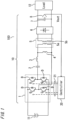
- FIG. 1 is a circuit diagram showing the configuration of a power conversion device according to Embodiment 1.
- a power conversion device 100 includes an LLC-type DC/DC converter 10 (hereinafter, referred to as LLC converter 10) connected between a DC power supply 11 and a load 12, and a controller 20 for performing output control of the LLC converter 10.
- LLC converter 10 an LLC-type DC/DC converter 10
- controller 20 for performing output control of the LLC converter 10.
- the LLC converter 10 includes an isolation transformer 5, and an inverter circuit 1 connected to a primary-side coil 5a of the isolation transformer 5.
- the LLC converter 10 includes, between the inverter circuit 1 and the primary-side coil 5a, a resonance capacitor 2 and a series resonance reactor 3 connected in series to the primary-side coil 5a, and a parallel resonance reactor 4 connected in parallel to the primary-side coil 5a.
- the LLC converter 10 includes an output circuit 6 which is connected to a secondary-side coil 5b of the isolation transformer 5 and rectifies output voltage, and a smoothing capacitor 7 connected in parallel at a stage subsequent to the output circuit 6.
- a voltage sensor 8 for detecting output voltage Vout of the LLC converter 10 is provided.
- the inverter circuit 1 is configured as a full-bridge circuit having a plurality of semiconductor switches Q.
- the semiconductor switches Q an insulated gate bipolar transistor (IGBT) to which a diode D is connected in antiparallel is used.
- IGBT insulated gate bipolar transistor
- MOSFET metal-oxide-semiconductor field-effect transistor
- the inverter circuit 1 is not limited to a full-bridge circuit and may be a half-bridge circuit.
- the output circuit 6 is configured as a diode bridge circuit, for example.
- the output circuit 6 may be a half-wave rectification type or a full-wave rectification type as long as inputted AC current can be rectified.
- the controller 20 receives output voltage Vout detected by the voltage sensor 8, and generates gate signals 21 for controlling the semiconductor switches Q of the inverter circuit 1 so that the output voltage Vout comes close to target voltage.
- the inverter circuit 1 is controlled by a combination of a switching frequency f (hereinafter, referred to as frequency f) and a phase shift amount ⁇ . That is, the controller 20 determines a combination of the frequency f and the phase shift amount ⁇ and generates the gate signals 21 to perform drive control of the inverter circuit 1, thus performing output control of the LLC converter 10.
- frequency f switching frequency
- phase shift amount ⁇ phase shift amount
- a resonance circuit composed of the resonance capacitor 2, the series resonance reactor 3, and the parallel resonance reactor 4 is provided between the inverter circuit 1 and the primary-side coil 5a. Then, using resonance of the resonance capacitor 2, the series resonance reactor 3, and the parallel resonance reactor 4, soft switching is performed in the inverter circuit 1, whereby switching loss can be reduced.
- the series resonance reactor 3 and the parallel resonance reactor 4 may be formed using a magnetizing inductance and a leakage inductance of the isolation transformer 5, as shown below.
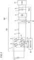
- FIG. 2 and FIG. 3 are circuit diagrams showing the configurations of the power conversion device according to other examples of Embodiment 1.
- the parallel resonance reactor and the isolation transformer 5 are formed integrally, and the magnetizing inductance of the isolation transformer 5 is used as the parallel resonance reactor.
- the inductance of the parallel resonance reactor 4 is smaller than the magnetizing inductance of the isolation transformer 5, and therefore the inductance of the parallel resonance reactor 4 influences resonance operation.
- the magnetizing inductance of the isolation transformer 5 determines resonance operation.
- the parallel resonance reactor, the series resonance reactor, and the isolation transformer 5 are integrated.
- the magnetizing inductance of the isolation transformer 5 is used as the parallel resonance reactor, and the leakage inductance of the isolation transformer 5 is used as the series resonance reactor.
- the load 12 supplied with power by the power conversion device 100 is a DC load such as a battery or a resistance load.
- the load 12 is a resistance load.
- the LLC converter 10 undergoes output control through switching operation of the inverter circuit 1 by the gate signals 21 from the controller 20.
- the LLC converter 10 converts DC power inputted from the DC power supply 11, to desired DC power (voltage, current), and supplies the converted DC power to the load 12.
- the inverter circuit 1 converts DC power supplied from the DC power supply 11, to rectangular-wave AC power, through switching operations of the semiconductor switches Q.
- Each semiconductor switch Q of the inverter circuit 1 is provided with a gate driving circuit (not shown), and the gate driving circuit receives the gate signal 21 from the controller 20 and drives a gate terminal of the semiconductor switch Q.
- the generated gate signal 21 has two degrees of freedom which are the frequency f and the phase shift amount ⁇ .
- the frequency f and the phase shift amount ⁇ By changing the frequency f and the phase shift amount ⁇ as appropriate, power to be supplied to the load 12 is controlled.
- FIG. 4 shows an output voltage waveform of the inverter circuit 1.
- the inverter circuit 1 outputs output voltage V-INV which is rectangular-wave voltage, on the basis of voltage VA of the DC power supply 11.
- the output voltage V-INV has three levels of +VA, 0, and -VA.
- the output voltage V-INV outputted from the inverter circuit 1 is inputted to the isolation transformer 5 through the series resonance reactor 3 and the parallel resonance reactor 4, and the resonance capacitor 2.
- resonance is caused by the series resonance reactor 3, the parallel resonance reactor 4, and the resonance capacitor 2, so that voltage not less than the output voltage V-INV of the inverter circuit 1 is inputted to the primary-side coil 5a of the isolation transformer 5.
- AC power inputted to the primary-side coil 5a of the isolation transformer 5 is supplied to the secondary-side coil 5b of the isolation transformer 5 and inputted to the output circuit 6. Then, the inputted power is rectified by the output circuit 6, to be converted to DC power. The DC power is smoothed by the smoothing capacitor 7 and then supplied to the load 12.
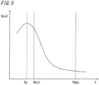
- a resonance system composed of the resonance capacitor 2, the series resonance reactor 3, and the parallel resonance reactor 4 is configured such that the output voltage Vout increases as the frequency f decreases, and the output voltage Vout decreases as the frequency f increases.
- FIG. 5 is a waveform graph showing the relationship between the frequency and the output voltage in the power conversion device 100.
- the resistance value of the load 12 is constant and the input voltage is also constant.
- a lower limit value fmin for the frequency f is set to be greater than a frequency fp at which the output voltage Vout is maximized.
- Increase/decrease of the phase shift amount ⁇ corresponds to substantial increase/decrease of the effective value of the output voltage V-INV of the inverter circuit 1, that is, the output voltage V-INV decreases as the phase shift amount ⁇ increases, and the output voltage V-INV increases as the phase shift amount ⁇ decreases.
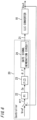
- FIG. 6 is a control block diagram of the power conversion device 100.
- the controller 20 receives output voltage Vout of the LLC converter 10 and calculates a deviation err between target voltage Vref and the output voltage Vout, and the deviation err is inputted to the control unit 22.
- the control unit 22 performs control calculation through PI (Proportional-Integral) control so that the inputted deviation err comes close to zero, and outputs a value Za of a manipulated variable Z.
- PI Proportional-Integral
- F(Z) ( ⁇ , f)
- the acquired combination ( ⁇ , f) is inputted to a gate signal generation circuit 24.
- the gate signal generation circuit 24 generates the gate signals 21 for the semiconductor switches Q of the inverter circuit 1 on the basis of the inputted phase shift amount ⁇ and frequency f, and the gate signals 21 are outputted from the controller 20.
- the inverter circuit 1 operates with the phase shift amount ⁇ and the frequency f provided by the gate signals 21 and thus the output voltage Vout of the LLC converter 10 is controlled.
- the entire range of the manipulated variable Z is constituted of consecutive integers from 0 to a maximum value Zmax.
- an upper limit value ⁇ max is 180°
- a lower limit value ⁇ min is 0°
- a set change width ⁇ which is change of the phase shift amount ⁇ per unit change amount 1 of the manipulated variable Z is 1°.
- an upper limit value fmax is 100 kHz
- a lower limit value fmin is 70 kHz
- a set change width ⁇ f which is change of the frequency f per unit change amount 1 of the manipulated variable Z is 0.1 kHz.
- the set change width ⁇ is not limited to 1°, and any possible step size for the phase shift amount ⁇ may be used. Also, the set change width ⁇ f is not limited to 0.1 kHz, and any possible step size for the frequency f may be used.
- the change amount of the manipulated variable Z corresponding to change of the phase shift amount ⁇ from the upper limit value ⁇ max (180°) to the lower limit value ⁇ min (0°) is 180
- the change amount of the manipulated variable Z corresponding to change of the frequency f from the upper limit value fmax (100 kHz) to the lower limit value fmin (70 kHz) is 300.
- the maximum value Zmax of the manipulated variable Z is 480, and the manipulated variable range is divided into a low manipulated variable range (0 to 180), and a high manipulated variable range (180 to 480) subsequent thereto.
- a border point Zx (180) between the two ranges is a point (integer) included in both of the low manipulated variable range (0 to 180) and the high manipulated variable range (180 to 480).
- the border point Zx (180) is the maximum value of the manipulated variable Z in the low manipulated variable range (0 to 180) and the minimum value thereof in the high manipulated variable range (180 to 480).
- the function F(Z) is set such that, in the low manipulated variable range (0 to 180) of the manipulated variable Z, the frequency f is kept at the upper limit value fmax and the phase shift amount ⁇ decreases by the set change width ⁇ from the upper limit value ⁇ max to the lower limit value ⁇ min per increase of the manipulated variable Z by 1.
- phase shift amount ⁇ continuously decreases by an equal set change width ⁇ (1°) per increase of the manipulated variable Z by 1.
- the function F(Z) is set such that, in the high manipulated variable range (180 to 480) of the manipulated variable Z, the phase shift amount ⁇ is kept at the lower limit value ⁇ min and the frequency f decreases by the set change width ⁇ f from the upper limit value fmax to the lower limit value fmin per increase of the manipulated variable Z by 1.
- the frequency f continuously decreases by an equal set change width ⁇ f (0.1 kHz) per increase of the manipulated variable Z by 1.
- the phase shift amount ⁇ is the lower limit value ⁇ min and the frequency f is the upper limit value fmax.
- a switching cycle (hereinafter, referred to as cycle) may be used instead of the frequency f.
- cycle a switching cycle
- a possible step size of the frequency f per minimum pulse resolution might not be constant, but a step size of the cycle (time resolution) is constant.
- phase shift amount ⁇ time corresponding to a degree may be used instead of a degree.
- the control unit 22 calculates the manipulated variable Z so that the deviation err between the target voltage Vref and the output voltage Vout becomes zero, in every control cycle.
- N denotes the present cycle
- N - 1 denotes the previous cycle
- the manipulated variable Z[N] can be calculated by the following expression.
- Z N Z N ⁇ 1 + kp ⁇ err N ⁇ err N ⁇ 1 + ki ⁇ err N + err N ⁇ 1 kp, ki: gain
- control calculation is merely an example.
- PI control has been shown as an example.
- control calculation may be performed by P (Proportional-Integral) control, PD (Proportional-Differential) control, PID (Proportional-Integral-Differential) control, or the like.
- the phase shift amount ⁇ and the frequency f are determined in the same manner in any case.
- phase shift amount ⁇ and the frequency f uniquely corresponding to the value Za of the manipulated variable Z is acquired and determined.
- the phase shift amount ⁇ and the frequency f can be easily and assuredly determined and control switching for a control mode or the like is not needed, whereby the LLC converter 10 can be controlled at high speed and stably.
- FIG. 8 illustrates control using the function F(Z) and shows the details of a part of FIG. 7 .
- both of the phase shift amount ⁇ and the frequency f may change in one control cycle. Also in this case, on the basis of the included function F(Z) set in advance, a combination ( ⁇ , f) of the phase shift amount ⁇ and the frequency f uniquely corresponding to the value Za of the manipulated variable Z is acquired, and thus the phase shift amount ⁇ and the frequency f can be easily and assuredly determined. In addition, since a control mode need not be switched, the LLC converter 10 can be controlled at high speed and stably.
- a combination ( ⁇ , f) of the phase shift amount ⁇ and the frequency f corresponding to the calculated value Za of the manipulated variable Z is acquired on the basis of the included function F(Z) set in advance.
- the controller 20 performs control calculation for the value Za of the manipulated variable Z so that the output voltage Vout comes close to the target voltage Vref, and acquires a combination ( ⁇ , f) of the phase shift amount ⁇ and the frequency f corresponding to the value Za of the manipulated variable Z, to perform drive control of the inverter circuit 1, thus controlling the LLC converter 10. Therefore, it is not necessary to switch the control mode and it is possible to achieve high-speed and stable control adaptable to a wide output voltage range.
- the controller 20 includes the function F(Z) for uniquely associating each value of the manipulated variable Z with a combination of the phase shift amount ⁇ and the frequency f, and acquires a combination ( ⁇ , f) of the phase shift amount ⁇ and the frequency f corresponding to the calculated value Za of the manipulated variable Z, on the basis of the function F(Z).
- a combination ( ⁇ , f) of the phase shift amount ⁇ and the frequency f can be easily and assuredly determined, and high-speed and stable control adaptable to a wide output voltage range can be easily achieved.
- Functions of the controller 20 are implemented by a processing circuit, for example.
- FIG. 9 is a block diagram showing an example of hardware for implementing functions of the controller 20.
- a processing circuit 200 forming the controller 20 is composed of a processor 201 and a storage device 202.
- the storage device 202 is provided with a volatile storage device such as a random access memory and a nonvolatile auxiliary storage device such as a flash memory (which are not shown). Instead of the flash memory, an auxiliary storage device of a hard disk may be provided.
- the processor 201 executes a program inputted from the storage device 202.
- the program is inputted from the auxiliary storage device to the processor 201 via the volatile storage device.
- the processor 201 may output data such as a calculation result to the volatile storage device of the storage device 202, or may store such data into the auxiliary storage device via the volatile storage device.
- processing circuit 200 a microcomputer or an FPGA described above is used, for example.
- the function F(Z) is set such that, in the entirety of the low manipulated variable range (0 to 180), the phase shift amount ⁇ continuously decreases by an equal set change width ⁇ (1°) per increase of the manipulated variable Z by 1.
- the frequency f continuously decreases by an equal set change width ⁇ f (0.1 kHz) per increase of the manipulated variable Z by 1.
- a first specific region where the phase shift amount ⁇ does not continuously decrease by an equal set change width ⁇ (1°), i.e., decreases discontinuously, is provided in the low manipulated variable range (0 to 180). Also in Embodiment 2, the power conversion device 100 having the same circuit configuration as in the above Embodiment 1 is applied.
- the LLC converter 10 is operated using the function F(Z) shown in FIG. 7 , and thereafter, the function F(Z) is changed in accordance with the operation state of the LLC converter 10 and the changed function Fa(Z) is set.
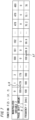
- FIG. 10 to FIG. 12 illustrate control according to Embodiment 2. Specifically, FIG. 10 shows waveforms at respective parts in a case of using the function F(Z) that has not been changed yet, FIG. 11 shows waveforms at respective parts in a case of using the changed function Fa(Z), and FIG. 12 shows change from the function F(Z) to the function Fa(Z).
- the controller 20 has such a function of storing, for example, a change amount of the output voltage Vout per control cycle, as a differential value of the output voltage Vout measured by the voltage sensor 8.
- the controller 20 To start supplying the gate signals 21 to the inverter circuit 1, the controller 20 generates the gate signals 21 in such a mode of sequentially increasing the manipulated variable Z, using the function F(Z) shown in the above Embodiment 1, thereby operating the LLC converter 10. At this time, a differential value dV/dt of the output voltage Vout is stored.
- the LLC converter 10 When the manipulated variable Z is sequentially increased using the function F(Z) as described above, the LLC converter 10 operates as shown in FIG. 10 .
- a waveform 31 represents change of the frequency f
- a waveform 32 represents change of the phase shift amount ⁇
- a waveform 33 represents change of the output voltage Vout
- a waveform 34 represents change of the differential value dV/dt of the output voltage Vout as an output differential value.
- the manipulated variable Z is an integer which is a discrete value
- the waveforms 31 to 34 of the frequency f, the phase shift amount ⁇ , the output voltage Vout, and the differential value dV/dt do not actually exhibit continuous changes, but are shown as lines connecting values, for convenience sake.
- the maximum value Zmax of the manipulated variable Z is 480, and in the graph, Z ⁇ is 170 and Z ⁇ is 180.
- the frequency f is kept at the upper limit value fmax and the phase shift amount ⁇ continuously decreases by the set change width ⁇ (1°) from the upper limit value ⁇ max to the lower limit value ⁇ min per increase of the manipulated variable Z by 1.
- the set change width ⁇ (1°) is defined as a unit change width ⁇ 1.
- the phase shift amount ⁇ is kept at the lower limit value ⁇ min and the frequency f continuously decreases by the set change width ⁇ f from the upper limit value fmax to the lower limit value fmin per increase of the manipulated variable Z by 1.
- the set change width ⁇ f (0.1 kHz) is defined as a unit change width ⁇ f1.
- the controller 20 detects a region A of the manipulated variables (Z ⁇ to Z ⁇ ) where the differential value dV/dt is not greater than a predetermined value Dth. Then, the function F(Z) is changed so as to exclude combinations ( ⁇ , f) of the phase shift amount ⁇ and the frequency f corresponding to the region A, and the changed function Fa(Z) is set.
- the frequency f, the phase shift amount ⁇ , the output voltage Vout, and the differential value dV/dt thereof shift from characteristics represented by the waveforms 31, 32, 33, 34 to characteristics represented by waveforms 31a, 32a, 33a, 34a.
- the waveforms 31a, 32a, 33a, 34a are formed such that a region of manipulated variables (Z ⁇ to Zmax) subsequent to the greater manipulated variable Z side of the detected region A of manipulated variables (Z ⁇ to Z ⁇ ), is shifted to the region A side.
- a combination ( ⁇ , f) of the phase shift amount ⁇ and the frequency f corresponding to the value Z ⁇ of the manipulated variable Z in the function F(Z) becomes a combination ( ⁇ , f) of the phase shift amount ⁇ and the frequency f corresponding to the value Z ⁇ of the manipulated variable Z in the new function Fa(Z).
- the manipulated variable Z is a discrete integer
- the manipulated variable region as a removal target corresponding to the region A is a region not less than Z ⁇ but less than Z ⁇ , and is actually a region of integers Z ⁇ to (Z ⁇ - 1).
- a phase shift amount ⁇ c at the lower limit value Z ⁇ of the manipulated variable Z in the region A is removed.
- combinations ( ⁇ , f) of the phase shift amount ⁇ and the frequency f in a region C of manipulated variables (180 to 480) subsequent to the region A in the function F(Z) become combinations ( ⁇ , f) of the phase shift amount ⁇ and the frequency f in a region Ca of manipulated variables (170 to 470) in the changed function Fa(Z).
- the frequency f is kept at the upper limit value fmax and the phase shift amount ⁇ decreases by the set change width ⁇ from the upper limit value ⁇ max to the lower limit value ⁇ min per increase of the manipulated variable Z by 1.
- the phase shift amount ⁇ continuously decreases by the unit change width ⁇ 1 per increase of the manipulated variable Z by 1.
- the region A where the differential value dV/dt of the output voltage Vout is not greater than a predetermined value Dth is detected, the function F(Z) is changed so as to exclude that region, and the changed function is used.
- a low-controllability range in which the output hardly changes relative to change of the manipulated variable Z can be removed, whereby control performance and response are improved.
- the LLC converter 10 is operated using the function F(Z) set in advance, the function F(Z) is changed in accordance with the operation state, and the changed function Fa(Z) is set.
- the function F(Z) can be changed as needed, and it is possible to dynamically set the first specific region X where the change width is not the unit change width ⁇ 1 (1°), by monitoring the differential value dV/dt of the output voltage Vout.
- the region A where the differential value dV/dt of the output voltage Vout is not greater than the set value Dth is detected, and the function F(Z) is changed so as to exclude that region.
- the function F(Z) can be changed in the same manner. In this case, the changed function is a function Fb(Z).
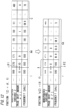
- FIG. 13 shows change from the function F(Z) to the function Fb(Z).
- the region A of manipulated variables (370 to 380).
- This region A is merely an example, and a region near the border between the low manipulated variable range (0 to 180) and the high manipulated variable range (180 to 480), e.g., a region (180 to 190), may be employed.
- the function F(Z) is changed so as to exclude the region A, i.e., so as to shift a region of manipulated variables (380 to 480) subsequent to the greater manipulated variable Z side of the region A to the region A side.
- the manipulated variable region as a removal target corresponding to the region A is actually a region of integers 370 to 379.
- combinations ( ⁇ , f) of the phase shift amount ⁇ and the frequency f in a region C of manipulated variables (380 to 480) subsequent to the region A (370 to 380) in the function F(Z) become combinations ( ⁇ , f) of the phase shift amount ⁇ and the frequency f in a region Ca of manipulated variables (370 to 470) in the changed function Fb(Z).
- combinations ( ⁇ , f) of the phase shift amount ⁇ and the frequency f in a region B of manipulated variables (0 to 369) in the function F(Z) are kept as they are, in the changed function Fb(Z).
- the frequency f is kept at the upper limit value fmax and the phase shift amount ⁇ decreases by the set change width ⁇ from the upper limit value ⁇ max to the lower limit value ⁇ min per increase of the manipulated variable Z by 1.
- the frequency f continuously decreases by the unit change width ⁇ f1 per increase of the manipulated variable Z by 1.
- the function F(Z) is changed to the function Fb(Z) so as to exclude that region, and the changed function Fb(Z) is used. In this way, a low-controllability range in which the output hardly changes relative to change of the manipulated variable Z can be removed, whereby control performance and response are improved.
- control frequency f since the range of the control frequency (frequency f) can be changed, the design range for the control frequency can be expanded, so that robustness is improved.
- the function F(Z) may be set in advance so that the differential value dV/dt of the output voltage Vout exceeds the set value Dth.
- the set function F(Z) includes one or both of the first specific region X and the second specific region Y, in advance.
- the differential value of output power or output current may be used as the output differential value.
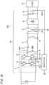
- FIG. 14 is a circuit diagram illustrating effects of the power conversion device according to Embodiment 2.
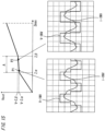
- FIG. 15 illustrates effects, using waveforms of output voltage and output current of the inverter circuit.
- the circuit configuration of the power conversion device 100 is the same as that shown in FIG. 1 , and in FIG. 14 , output voltage V-INV and output current i-INV of the inverter circuit 1 are shown.
- FIG. 15 the output voltage V-INV and the output current i-INV at two points P1 and P2 in the region A of manipulated variables (Z ⁇ to Z ⁇ ) where the differential value dV/dt is not greater than the set value Dth and the output voltage Vout hardly changes, are shown.
- the manipulated variable Z is Z ⁇
- the ratio of output voltage V-Z ⁇ to the input (input-output voltage ratio) is 0.84
- the manipulated variable Z is Z ⁇
- the ratio of output voltage V-Z ⁇ to the input (input-output voltage ratio) is 0.85.
- a period in which the signs of the output voltage V-INV and the output current i-INV are opposite to each other is long, that is, a period in which reactive power is outputted is long.
- the output voltage Vout of the LLC converter 10 hardly changes.
- Embodiment 2 the region A which is an operation range where control performance is deteriorated as described above can be detected and removed. Thus, an effect of improving control performance and improving response is obtained.
- the operation range where control performance is deteriorated changes depending on the state of the connected load 12. Further, the operation range where control performance is deteriorated might also change depending on the resonance characteristic of the resonance circuit composed of the resonance capacitor 2, the series resonance reactor 3, and the parallel resonance reactor 4, variations in elements of the resonance circuit, or the like.
- a range of the manipulated variable Z to be removed as a region where the differential value dV/dt of the output voltage Vout is not greater than the set value Dth is an end range on the greater manipulated variable Z side in the entire range (0 to 480).
- the LLC converter 10 is operated using the function F(Z) shown in FIG. 7 , and thereafter, the function F(Z) is changed in accordance with the operation state of the LLC converter 10.
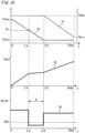
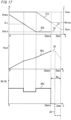
- FIG. 16 and FIG. 17 show waveforms at respective parts for illustrating control according to Embodiment 3. Specifically, FIG. 16 shows waveforms at respective parts in a case of using the function F(Z) that has not been changed yet, and FIG. 17 shows waveforms at respective parts in a case of using the changed function F(Z).
- the controller 20 to start supplying the gate signals 21 to the inverter circuit 1, the controller 20 generates the gate signals 21 in such a mode of sequentially increasing the manipulated variable Z, using the function F(Z) shown in the above Embodiment 1, thereby operating the LLC converter 10. At this time, the differential value dV/dt of the output voltage Vout is stored.
- the LLC converter 10 When the manipulated variable Z is sequentially increased using the function F(Z) as described above, in this case, the LLC converter 10 operates as shown in FIG. 16 .
- a waveform 31 represents change of the frequency f
- a waveform 32 represents change of the phase shift amount ⁇
- a waveform 35 represents change of the output voltage Vout
- a waveform 36 represents change of the differential value dV/dt of the output voltage Vout.
- the manipulated variable Z is an integer which is a discrete value
- the waveforms 31 to 34 of the frequency f, the phase shift amount ⁇ , the output voltage Vout, and the differential value dV/dt thereof do not actually exhibit continuous changes, but are shown as lines connecting values, for convenience sake.
- the maximum value Zmax of the manipulated variable Z is 480.
- the differential value dV/dt of the output voltage Vout might be reduced or become negative. That is, even if the manipulated variable Z is increased, the output voltage Vout does not increase and is reduced thereafter.
- the set value is set at 0, a region Aa where the differential value dV/dt is not greater than the set value 0 is detected, and the function F(Z) is changed so as to exclude the region Aa.
- the frequency f, the phase shift amount ⁇ , the output voltage Vout, and the differential value dV/dt thereof shift from characteristics represented by the waveforms 31, 32, 35, 36 to characteristics represented by waveforms 31b, 32b, 35a, 36a.
- the waveforms 31b, 32b, 35a, 36a are formed with the detected region Aa merely removed from the waveforms 31, 32, 35, 36, the maximum value Zmax of the manipulated variable Z decreases by the number of the removed manipulated variables Z, to become the maximum value Zmaxa, and the lower limit value fmin of the frequency f is changed to a lower limit value fmina.
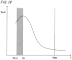
- FIG. 18 is a waveform graph illustrating the relationship between the frequency and the output voltage.
- the lower limit value fmin for the frequency f is set to be smaller than the frequency fp at which the output voltage Vout is maximized. Then, by changing the function F(Z), a hatched range from the lower limit value fmin to the frequency fp is removed from the control range.
- the region Aa where the differential value dV/dt of the output voltage Vout is not greater than a predetermined value 0 is detected, the function F(Z) is changed so as to exclude that region, and the changed function is used.
- the function F(Z) is changed so as to exclude that region, and the changed function is used.
- the proportional relationship means that, under a condition that the impedance of the output voltage Vout is constant, the output voltage Vout increases with increase of the manipulated variable Z, and the output voltage Vout decreases with decrease of the manipulated variable Z. It becomes possible to perform more appropriate control by keeping the above proportional relationship.
- the lower limit value fmin and the upper limit value fmax for the frequency f are set, and the frequency f is set so that the output is maximized at the lower limit value fmin and the output is minimized at the upper limit value fmax.
- the circuit constants are set such that the increase/decrease relationship between the frequency f and the output voltage Vout is not inverted, and control operation is performed in such a range.
- the circuit constants or control is designed so that the LLC converter 10 is not operated in the range where the increase/decrease relationship between the frequency f and the output voltage Vout is inverted.
- the lower limit value fmin for the frequency f is set to be high, so that the adaptable load range, output, or error tolerance for the circuit constants is reduced.
- FIG. 19 illustrates an operation range and the relationship between the frequency and the output voltage under two load conditions.
- a frequency fpX corresponding to a peak is, for example, 70 kHz
- a frequency fpY corresponding to a peak is, for example, 75 kHz.
- the lower limit value fmin for the frequency f is set at, for example, 76 kHz, the output voltage 38X under the first load condition is low in a set operation range Rf, so that desired output voltage 38X cannot be obtained.
- the frequencies fpX, fpY corresponding to peaks are determined by parameters of elements of the resonance circuit composed of the resonance capacitor 2, the series resonance reactor 3, and the parallel resonance reactor 4, and therefore are also influenced by error or variation in constants thereof.
- the lower limit value fmin for the frequency f is set with tolerable error or load variation taken into consideration, but as a result, the lower limit value fmin for the frequency f is set to be high, so that the control range is reduced and robustness is also reduced.
- the region Aa where the differential value dV/dt of the output voltage Vout is not greater than a predetermined value 0 is detected and the function F(Z) is changed so as to exclude that region, whereby the maximum value Zmax of the manipulated variable Z and the lower limit value fmin for the frequency f can be changed.
Landscapes
- Engineering & Computer Science (AREA)
- Power Engineering (AREA)
- Dc-Dc Converters (AREA)
Applications Claiming Priority (1)
| Application Number | Priority Date | Filing Date | Title |
|---|---|---|---|
| PCT/JP2021/024692 WO2023276024A1 (fr) | 2021-06-30 | 2021-06-30 | Dispositif de conversion de puissance |
Publications (2)
| Publication Number | Publication Date |
|---|---|
| EP4366149A1 true EP4366149A1 (fr) | 2024-05-08 |
| EP4366149A4 EP4366149A4 (fr) | 2024-08-28 |
Family
ID=84691628
Family Applications (1)
| Application Number | Title | Priority Date | Filing Date |
|---|---|---|---|
| EP21948331.0A Withdrawn EP4366149A4 (fr) | 2021-06-30 | 2021-06-30 | Dispositif de conversion de puissance |
Country Status (4)
| Country | Link |
|---|---|
| US (1) | US20240235403A1 (fr) |
| EP (1) | EP4366149A4 (fr) |
| JP (1) | JP7542746B2 (fr) |
| WO (1) | WO2023276024A1 (fr) |
Families Citing this family (1)
| Publication number | Priority date | Publication date | Assignee | Title |
|---|---|---|---|---|
| WO2024257394A1 (fr) * | 2023-06-12 | 2024-12-19 | パナソニックIpマネジメント株式会社 | Circuit de commande, convertisseur de puissance électrique et procédé de commande |
Family Cites Families (36)
| Publication number | Priority date | Publication date | Assignee | Title |
|---|---|---|---|---|
| US4951185A (en) * | 1989-07-13 | 1990-08-21 | General Electric Company | Resonant inverter employing frequency and phase modulation using optimal trajectory control |
| CN101056061B (zh) * | 2006-04-14 | 2012-12-05 | 艾默生网络能源系统北美公司 | 一种谐振电路调制控制方法和系统 |
| CN101064476B (zh) * | 2006-04-30 | 2012-06-27 | 艾默生网络能源系统北美公司 | 一种谐振直流/直流变换器及其控制方法 |
| TWI340528B (en) * | 2007-04-03 | 2011-04-11 | Delta Electronics Inc | Resonant converter system and controlling method thereof having relatively better efficiency |
| US8717783B2 (en) * | 2009-10-30 | 2014-05-06 | Delta Electronics (Shanghai) Co., Ltd. | Method and apparatus for regulating gain within a resonant converter |
| US9379617B2 (en) * | 2012-02-03 | 2016-06-28 | Fuji Electric Co., Ltd. | Resonant DC-DC converter control device |
| EP2940848B1 (fr) * | 2012-12-28 | 2018-12-05 | Panasonic Intellectual Property Management Co., Ltd. | Convertisseur cc/cc |
| WO2015004989A1 (fr) * | 2013-07-11 | 2015-01-15 | 富士電機株式会社 | Convertisseur continu-continu bidirectionnel |
| US10707775B2 (en) * | 2013-08-14 | 2020-07-07 | Enphase Energy, Inc. | Method and apparatus for multi phase shift power converter control |
| US9490704B2 (en) * | 2014-02-12 | 2016-11-08 | Delta Electronics, Inc. | System and methods for controlling secondary side switches in resonant power converters |
| US9509225B2 (en) | 2014-09-16 | 2016-11-29 | Continental Automotive Systems, Inc. | Efficient LLC resonant converter having variable frequency control and fixed frequency phase-shift PWM |
| US9595867B2 (en) * | 2014-10-02 | 2017-03-14 | Texas Instruments Incorporated | System and method to improve standby efficiency of LLC converter |
| JP6153144B1 (ja) * | 2016-03-17 | 2017-06-28 | 三菱電機株式会社 | Dc/dcコンバータの制御装置および制御方法 |
| US11063520B2 (en) * | 2016-12-16 | 2021-07-13 | Murata Manufacturing Co., Ltd. | Simplified hybrid PWM/PFM control method for SLLC converter |
| JP6381853B1 (ja) * | 2017-04-03 | 2018-08-29 | 三菱電機株式会社 | 電力変換装置 |
| CN107809178B (zh) * | 2017-11-03 | 2021-06-11 | 上海联影医疗科技股份有限公司 | 一种高压发生器及其控制方法 |
| US11056979B2 (en) * | 2017-12-25 | 2021-07-06 | Mitsubishi Electric Corporation | Power conversion apparatus |
| JP7061548B2 (ja) * | 2018-10-04 | 2022-04-28 | 株式会社日立産機システム | 共振型電源装置 |
| JP2020124050A (ja) * | 2019-01-31 | 2020-08-13 | 株式会社デンソー | 共振インバータ装置 |
| KR102829319B1 (ko) * | 2019-05-20 | 2025-07-02 | 현대자동차주식회사 | Llc 공진 컨버터 및 이를 포함하는 충전 시스템 |
| US11025172B2 (en) * | 2019-08-26 | 2021-06-01 | Delta Electronics, Inc. | Three-level modulation for wide output voltage range isolated DC/DC converters |
| US11901826B2 (en) * | 2019-08-26 | 2024-02-13 | Delta Electronics, Inc. | Isolated DC/DC converters for wide output voltage range and control methods thereof |
| US20220337166A1 (en) * | 2019-09-05 | 2022-10-20 | Hong Kong Applied Science and Technology Research Institute Company Limited | Adaptive Power Control for Two-Stage AC/DC or DC/DC Isolated Power Converters |
| WO2021071708A1 (fr) * | 2019-10-11 | 2021-04-15 | Virginia Tech Intellectual Properties Inc. | Convertisseurs cc-ca commandés par modulation hybride |
| CN111864915B (zh) * | 2020-07-27 | 2021-03-12 | 北京理工大学 | 宽功率范围内实现zvs的无线充电系统调控方法及系统 |
| US11689092B1 (en) * | 2020-09-25 | 2023-06-27 | Imagen Energy, LLC | Grid connected three phase PV power conversion system utilizing adaptive LLC resonant inverter, high frequency isolation transformer, modular unfolding inverter, and controller |
| CN114362532A (zh) * | 2020-09-30 | 2022-04-15 | 台达电子工业股份有限公司 | Llc谐振转换器及其控制方法 |
| CN114362533B (zh) * | 2020-09-30 | 2025-08-19 | 台达电子工业股份有限公司 | Llc谐振转换器、控制单元及其控制方法 |
| WO2022130612A1 (fr) * | 2020-12-18 | 2022-06-23 | 三菱電機株式会社 | Dispositif de conversion de puissance |
| JP7541298B2 (ja) * | 2021-01-13 | 2024-08-28 | 富士電機株式会社 | 電力変換装置、電力変換装置の制御装置、および、電力変換制御方法 |
| JP7387663B2 (ja) * | 2021-03-02 | 2023-11-28 | 株式会社東芝 | 電力変換回路及び電力変換装置 |
| CN114301297B (zh) * | 2021-06-23 | 2024-06-25 | 华为数字能源技术有限公司 | 一种功率变换器、增大逆向增益范围的方法、装置、介质 |
| CN115528918B (zh) * | 2021-06-25 | 2026-07-28 | 台达电子工业股份有限公司 | Llc谐振转换器及其控制方法 |
| CN116247937A (zh) * | 2021-12-07 | 2023-06-09 | 台达电子企业管理(上海)有限公司 | 一种谐振变换器及谐振变换器控制方法 |
| EP4254759A1 (fr) * | 2022-03-31 | 2023-10-04 | Watt & Well | Convertisseur cc/cc de chargeurs de batteries et procédé de commande d'un tel convertisseur cc/cc dans des conditions de charge très légère |
| JP2024134687A (ja) * | 2023-03-22 | 2024-10-04 | パナソニックオートモーティブシステムズ株式会社 | 電力変換装置、車両、制御方法およびプログラム |
-
2021
- 2021-06-30 EP EP21948331.0A patent/EP4366149A4/fr not_active Withdrawn
- 2021-06-30 US US18/572,220 patent/US20240235403A1/en not_active Abandoned
- 2021-06-30 JP JP2023531223A patent/JP7542746B2/ja active Active
- 2021-06-30 WO PCT/JP2021/024692 patent/WO2023276024A1/fr not_active Ceased
Also Published As
| Publication number | Publication date |
|---|---|
| JP7542746B2 (ja) | 2024-08-30 |
| WO2023276024A1 (fr) | 2023-01-05 |
| US20240235403A1 (en) | 2024-07-11 |
| EP4366149A4 (fr) | 2024-08-28 |
| JPWO2023276024A1 (fr) | 2023-01-05 |
Similar Documents
| Publication | Publication Date | Title |
|---|---|---|
| US7683568B2 (en) | Motor drive using flux adjustment to control power factor | |
| CN107809178B (zh) | 一种高压发生器及其控制方法 | |
| EP1589650B1 (fr) | Commande de moteur | |
| US11056979B2 (en) | Power conversion apparatus | |
| KR20240035881A (ko) | 제로-시퀀스 안정화된 전력 변환기들의 제어를 위한 시스템들 및 방법들 | |
| CN116530004B (zh) | 电力变换装置 | |
| US20100214809A1 (en) | Pwm rectifier | |
| CN102986127B (zh) | 循环变流器的前馈控制 | |
| EP2461473A2 (fr) | Alimentation controllée par modulation de largeur d'impulsion et modulation de phase | |
| US11368109B2 (en) | Power conversion system with PWM carrier transition smoothing and autotuning | |
| JP6381497B2 (ja) | 電力変換装置 | |
| EP1548923B1 (fr) | Dispositif et procédé de commande pour onduleur | |
| EP4420229B1 (fr) | Convertisseur de puissance c.c.-c.c. à résonance en série basé sur une commande multimode et méthode de commande | |
| JP6366543B2 (ja) | Dc/dcコンバータ | |
| Divakar et al. | Genetic algorithm based tuning of nonfragile and robust PI controller for PSFB DC-DC converter | |
| US20240235403A1 (en) | Power conversion device | |
| US11296608B2 (en) | Electric-power conversion apparatus | |
| JP2004072806A (ja) | 電力変換装置 | |
| US11456690B2 (en) | Pulse-controlled inverter with a variable speed-dependent switching frequency | |
| JP7109688B2 (ja) | 電力変換装置 | |
| CN110739852B (zh) | 谐振电源及其控制方法以及非暂态计算机可读存储介质 | |
| JP2017070056A (ja) | インバータ駆動装置 | |
| JP7825700B2 (ja) | 電力変換方法及び電力変換装置 | |
| US12525864B2 (en) | Method for compensating reactive power, associated control system, and sensor driver circuit | |
| KR20210029546A (ko) | 파워 변환 장치 및 이의 동작 방법 |
Legal Events
| Date | Code | Title | Description |
|---|---|---|---|
| STAA | Information on the status of an ep patent application or granted ep patent |
Free format text: STATUS: THE INTERNATIONAL PUBLICATION HAS BEEN MADE |
|
| PUAI | Public reference made under article 153(3) epc to a published international application that has entered the european phase |
Free format text: ORIGINAL CODE: 0009012 |
|
| STAA | Information on the status of an ep patent application or granted ep patent |
Free format text: STATUS: REQUEST FOR EXAMINATION WAS MADE |
|
| 17P | Request for examination filed |
Effective date: 20231220 |
|
| AK | Designated contracting states |
Kind code of ref document: A1 Designated state(s): AL AT BE BG CH CY CZ DE DK EE ES FI FR GB GR HR HU IE IS IT LI LT LU LV MC MK MT NL NO PL PT RO RS SE SI SK SM TR |
|
| REG | Reference to a national code |
Ref country code: DE Ref legal event code: R079 Free format text: PREVIOUS MAIN CLASS: H02M0003280000 Ipc: H02M0001000000 |
|
| A4 | Supplementary search report drawn up and despatched |
Effective date: 20240726 |
|
| RIC1 | Information provided on ipc code assigned before grant |
Ipc: H02M 7/5387 20070101ALI20240722BHEP Ipc: H02M 3/335 20060101ALI20240722BHEP Ipc: H02M 3/00 20060101ALI20240722BHEP Ipc: H02M 1/00 20060101AFI20240722BHEP |
|
| DAV | Request for validation of the european patent (deleted) | ||
| DAX | Request for extension of the european patent (deleted) | ||
| STAA | Information on the status of an ep patent application or granted ep patent |
Free format text: STATUS: THE APPLICATION HAS BEEN WITHDRAWN |
|
| 18W | Application withdrawn |
Effective date: 20251204 |