EP4369252B1 - Précision dynamique pour opérations de calcul de réseau neuronal - Google Patents
Précision dynamique pour opérations de calcul de réseau neuronal Download PDFInfo
- Publication number
- EP4369252B1 EP4369252B1 EP24166744.3A EP24166744A EP4369252B1 EP 4369252 B1 EP4369252 B1 EP 4369252B1 EP 24166744 A EP24166744 A EP 24166744A EP 4369252 B1 EP4369252 B1 EP 4369252B1
- Authority
- EP
- European Patent Office
- Prior art keywords
- graphics
- processor
- memory
- data
- processing
- Prior art date
- Legal status (The legal status is an assumption and is not a legal conclusion. Google has not performed a legal analysis and makes no representation as to the accuracy of the status listed.)
- Active
Links
Images












Classifications
-
- G—PHYSICS
- G06—COMPUTING OR CALCULATING; COUNTING
- G06N—COMPUTING ARRANGEMENTS BASED ON SPECIFIC COMPUTATIONAL MODELS
- G06N3/00—Computing arrangements based on biological models
- G06N3/02—Neural networks
- G06N3/06—Physical realisation, i.e. hardware implementation of neural networks, neurons or parts of neurons
- G06N3/063—Physical realisation, i.e. hardware implementation of neural networks, neurons or parts of neurons using electronic means
-
- G—PHYSICS
- G06—COMPUTING OR CALCULATING; COUNTING
- G06F—ELECTRIC DIGITAL DATA PROCESSING
- G06F1/00—Details not covered by groups G06F3/00 - G06F13/00 and G06F21/00
- G06F1/26—Power supply means, e.g. regulation thereof
- G06F1/32—Means for saving power
- G06F1/3203—Power management, i.e. event-based initiation of a power-saving mode
- G06F1/3234—Power saving characterised by the action undertaken
- G06F1/3287—Power saving characterised by the action undertaken by switching off individual functional units in the computer system
-
- G—PHYSICS
- G06—COMPUTING OR CALCULATING; COUNTING
- G06F—ELECTRIC DIGITAL DATA PROCESSING
- G06F1/00—Details not covered by groups G06F3/00 - G06F13/00 and G06F21/00
- G06F1/26—Power supply means, e.g. regulation thereof
- G06F1/32—Means for saving power
- G06F1/3203—Power management, i.e. event-based initiation of a power-saving mode
- G06F1/3234—Power saving characterised by the action undertaken
- G06F1/3293—Power saving characterised by the action undertaken by switching to a less power-consuming processor, e.g. sub-CPU
-
- G—PHYSICS
- G06—COMPUTING OR CALCULATING; COUNTING
- G06F—ELECTRIC DIGITAL DATA PROCESSING
- G06F15/00—Digital computers in general; Data processing equipment in general
- G06F15/76—Architectures of general purpose stored program computers
-
- G—PHYSICS
- G06—COMPUTING OR CALCULATING; COUNTING
- G06F—ELECTRIC DIGITAL DATA PROCESSING
- G06F15/00—Digital computers in general; Data processing equipment in general
- G06F15/76—Architectures of general purpose stored program computers
- G06F15/78—Architectures of general purpose stored program computers comprising a single central processing unit
-
- G—PHYSICS
- G06—COMPUTING OR CALCULATING; COUNTING
- G06F—ELECTRIC DIGITAL DATA PROCESSING
- G06F9/00—Arrangements for program control, e.g. control units
- G06F9/06—Arrangements for program control, e.g. control units using stored programs, i.e. using an internal store of processing equipment to receive or retain programs
- G06F9/30—Arrangements for executing machine instructions, e.g. instruction decode
- G06F9/30003—Arrangements for executing specific machine instructions
- G06F9/30007—Arrangements for executing specific machine instructions to perform operations on data operands
- G06F9/3001—Arithmetic instructions
- G06F9/30014—Arithmetic instructions with variable precision
-
- G—PHYSICS
- G06—COMPUTING OR CALCULATING; COUNTING
- G06F—ELECTRIC DIGITAL DATA PROCESSING
- G06F9/00—Arrangements for program control, e.g. control units
- G06F9/06—Arrangements for program control, e.g. control units using stored programs, i.e. using an internal store of processing equipment to receive or retain programs
- G06F9/30—Arrangements for executing machine instructions, e.g. instruction decode
- G06F9/30003—Arrangements for executing specific machine instructions
- G06F9/30007—Arrangements for executing specific machine instructions to perform operations on data operands
- G06F9/30036—Instructions to perform operations on packed data, e.g. vector, tile or matrix operations
-
- G—PHYSICS
- G06—COMPUTING OR CALCULATING; COUNTING
- G06F—ELECTRIC DIGITAL DATA PROCESSING
- G06F9/00—Arrangements for program control, e.g. control units
- G06F9/06—Arrangements for program control, e.g. control units using stored programs, i.e. using an internal store of processing equipment to receive or retain programs
- G06F9/30—Arrangements for executing machine instructions, e.g. instruction decode
- G06F9/30003—Arrangements for executing specific machine instructions
- G06F9/30007—Arrangements for executing specific machine instructions to perform operations on data operands
- G06F9/30036—Instructions to perform operations on packed data, e.g. vector, tile or matrix operations
- G06F9/30038—Instructions to perform operations on packed data, e.g. vector, tile or matrix operations using a mask
-
- G—PHYSICS
- G06—COMPUTING OR CALCULATING; COUNTING
- G06N—COMPUTING ARRANGEMENTS BASED ON SPECIFIC COMPUTATIONAL MODELS
- G06N3/00—Computing arrangements based on biological models
- G06N3/02—Neural networks
- G06N3/04—Architecture, e.g. interconnection topology
- G06N3/044—Recurrent networks, e.g. Hopfield networks
-
- G—PHYSICS
- G06—COMPUTING OR CALCULATING; COUNTING
- G06N—COMPUTING ARRANGEMENTS BASED ON SPECIFIC COMPUTATIONAL MODELS
- G06N3/00—Computing arrangements based on biological models
- G06N3/02—Neural networks
- G06N3/04—Architecture, e.g. interconnection topology
- G06N3/044—Recurrent networks, e.g. Hopfield networks
- G06N3/0442—Recurrent networks, e.g. Hopfield networks characterised by memory or gating, e.g. long short-term memory [LSTM] or gated recurrent units [GRU]
-
- G—PHYSICS
- G06—COMPUTING OR CALCULATING; COUNTING
- G06N—COMPUTING ARRANGEMENTS BASED ON SPECIFIC COMPUTATIONAL MODELS
- G06N3/00—Computing arrangements based on biological models
- G06N3/02—Neural networks
- G06N3/04—Architecture, e.g. interconnection topology
- G06N3/045—Combinations of networks
-
- G—PHYSICS
- G06—COMPUTING OR CALCULATING; COUNTING
- G06N—COMPUTING ARRANGEMENTS BASED ON SPECIFIC COMPUTATIONAL MODELS
- G06N3/00—Computing arrangements based on biological models
- G06N3/02—Neural networks
- G06N3/04—Architecture, e.g. interconnection topology
- G06N3/0464—Convolutional networks [CNN, ConvNet]
-
- G—PHYSICS
- G06—COMPUTING OR CALCULATING; COUNTING
- G06N—COMPUTING ARRANGEMENTS BASED ON SPECIFIC COMPUTATIONAL MODELS
- G06N3/00—Computing arrangements based on biological models
- G06N3/02—Neural networks
- G06N3/08—Learning methods
-
- G—PHYSICS
- G06—COMPUTING OR CALCULATING; COUNTING
- G06N—COMPUTING ARRANGEMENTS BASED ON SPECIFIC COMPUTATIONAL MODELS
- G06N3/00—Computing arrangements based on biological models
- G06N3/02—Neural networks
- G06N3/08—Learning methods
- G06N3/084—Backpropagation, e.g. using gradient descent
-
- G—PHYSICS
- G06—COMPUTING OR CALCULATING; COUNTING
- G06N—COMPUTING ARRANGEMENTS BASED ON SPECIFIC COMPUTATIONAL MODELS
- G06N3/00—Computing arrangements based on biological models
- G06N3/02—Neural networks
- G06N3/08—Learning methods
- G06N3/0895—Weakly supervised learning, e.g. semi-supervised or self-supervised learning
-
- G—PHYSICS
- G06—COMPUTING OR CALCULATING; COUNTING
- G06N—COMPUTING ARRANGEMENTS BASED ON SPECIFIC COMPUTATIONAL MODELS
- G06N3/00—Computing arrangements based on biological models
- G06N3/02—Neural networks
- G06N3/08—Learning methods
- G06N3/09—Supervised learning
-
- G—PHYSICS
- G06—COMPUTING OR CALCULATING; COUNTING
- G06N—COMPUTING ARRANGEMENTS BASED ON SPECIFIC COMPUTATIONAL MODELS
- G06N3/00—Computing arrangements based on biological models
- G06N3/02—Neural networks
- G06N3/08—Learning methods
- G06N3/098—Distributed learning, e.g. federated learning
-
- G—PHYSICS
- G06—COMPUTING OR CALCULATING; COUNTING
- G06T—IMAGE DATA PROCESSING OR GENERATION, IN GENERAL
- G06T1/00—General purpose image data processing
- G06T1/20—Processor architectures; Processor configuration, e.g. pipelining
-
- G—PHYSICS
- G06—COMPUTING OR CALCULATING; COUNTING
- G06T—IMAGE DATA PROCESSING OR GENERATION, IN GENERAL
- G06T15/00—Three-dimensional [3D] image rendering
- G06T15/005—General purpose rendering architectures
-
- G—PHYSICS
- G06—COMPUTING OR CALCULATING; COUNTING
- G06T—IMAGE DATA PROCESSING OR GENERATION, IN GENERAL
- G06T1/00—General purpose image data processing
- G06T1/60—Memory management
-
- Y—GENERAL TAGGING OF NEW TECHNOLOGICAL DEVELOPMENTS; GENERAL TAGGING OF CROSS-SECTIONAL TECHNOLOGIES SPANNING OVER SEVERAL SECTIONS OF THE IPC; TECHNICAL SUBJECTS COVERED BY FORMER USPC CROSS-REFERENCE ART COLLECTIONS [XRACs] AND DIGESTS
- Y02—TECHNOLOGIES OR APPLICATIONS FOR MITIGATION OR ADAPTATION AGAINST CLIMATE CHANGE
- Y02D—CLIMATE CHANGE MITIGATION TECHNOLOGIES IN INFORMATION AND COMMUNICATION TECHNOLOGIES [ICT], I.E. INFORMATION AND COMMUNICATION TECHNOLOGIES AIMING AT THE REDUCTION OF THEIR OWN ENERGY USE
- Y02D10/00—Energy efficient computing, e.g. low power processors, power management or thermal management
Definitions
- Machine learning has been successful at solving many kinds of tasks.
- the computations that arise when training and using machine learning algorithms lend themselves naturally to efficient parallel implementations.
- parallel processors such as general-purpose graphic processing units (GPGPUs) have played a significant role in the practical implementation of deep neural networks.
- graphics processors with single instruction, multiple thread (SIMT) architectures are designed to maximize the amount of parallel processing in the graphics pipeline.
- SIMT single instruction, multiple thread
- groups of parallel threads attempt to execute program instructions synchronously together as often as possible to increase processing efficiency.
- the efficiency provided by parallel machine learning algorithm implementations allows the use of high capacity networks and enables those networks to be trained on larger datasets.
- US2014282593 A1 relates to scheduling threads in a multicore processor.
- an apparatus comprises a compute engine comprising a high precision component and a low precision component; and logic, at least partially including hardware logic, to receive instructions in the compute engine; and select at least one of the high precision component or the low precision component to execute the instructions; and apply a gate to at least one of the high precision component or the low precision component to execute the instructions
- the gate comprises a clock gate or a power gate.
- the literal wording of the claims granted an apparatus comprises logic, at least partially including hardware logic, to track a precision level data of neural network operations; and expose the precision level data in a model specific register.
- an apparatus comprises a low-level training pipeline; a high-level training pipeline; and logic, at least partially including hardware logic, to transfer training signals which generate an error in the low-level training pipeline to the high-level training pipeline.
- processors such as GPCPU, CPU, GPU, etc.
- graphics controllers etc.
- Other embodiments are also disclosed and claimed.
- processors e.g., with one or more processor cores
- mobile computing devices e.g., a smartphone, tablet, UMPC (Ultra-Mobile Personal Computer), laptop computer, Ultrabook TM computing device, wearable devices (such as a smart watch or smart glasses), etc.
- UMPC Ultra-Mobile Personal Computer
- Ultrabook TM computing device wearable devices (such as a smart watch or smart glasses), etc.
- a graphics processing unit is communicatively coupled to host/processor cores to accelerate graphics operations, machine-learning operations, pattern analysis operations, and various general purpose GPU (GPGPU) functions.
- the GPU may be communicatively coupled to the host processor/cores over a bus or another interconnect (e.g., a high-speed interconnect such as PCIe or NVLink).
- the GPU may be integrated on the same package or chip as the cores and communicatively coupled to the cores over an internal processor bus/interconnect (i.e., internal to the package or chip).
- the processor cores may allocate work to the GPU in the form of sequences of commands/instructions contained in a work descriptor.
- the GPU then uses dedicated circuitry/logic for efficiently processing these commands/instructions.
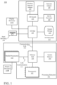
- FIG. 1 is a block diagram illustrating a computing system 100 configured to implement one or more aspects described herein.
- the computing system 100 includes a processing subsystem 101 having one or more processor(s) 102 and a system memory 104 communicating via an interconnection path that may include a memory hub 105.
- the memory hub 105 may be a separate component within a chipset component or may be integrated within the one or more processor(s) 102.
- the memory hub 105 couples with an I/O subsystem 111 via a communication link 106.
- the I/O subsystem 111 includes an I/O hub 107 that can enable the computing system 100 to receive input from one or more input device(s) 108.
- the I/O hub 107 can enable a display controller, which may be included in the one or more processor(s) 102, to provide outputs to one or more display device(s) 110A.
- the one or more display device(s) 110A coupled with the I/O hub 107 can include a local, internal, or embedded display device.
- the one or more parallel processor(s) 112 incorporate circuitry optimized for graphics and video processing, including, for example, video output circuitry, and constitutes a graphics processing unit (GPU).
- the one or more parallel processor(s) 112 incorporate circuitry optimized for general purpose processing, while preserving the underlying computational architecture, described in greater detail herein.
- components of the computing system 100 may be integrated with one or more other system elements on a single integrated circuit.
- the one or more parallel processor(s), 112 memory hub 105, processor(s) 102, and I/O hub 107 can be integrated into a system on chip (SoC) integrated circuit.
- SoC system on chip
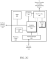
- the instruction cache 252 receives a stream of instructions to execute from the pipeline manager 232.
- the instructions are cached in the instruction cache 252 and dispatched for execution by the instruction unit 254.
- the instruction unit 254 can dispatch instructions as thread groups (e.g., warps), with each thread of the thread group assigned to a different execution unit within GPGPU core 262.
- An instruction can access any of a local, shared, or global address space by specifying an address within a unified address space.
- the address mapping unit 256 can be used to translate addresses in the unified address space into a distinct memory address that can be accessed by the load/store units 266.
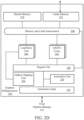
- the register file 258 provides a set of registers for the functional units of the graphics multiprocessor 324.
- the register file 258 provides temporary storage for operands connected to the data paths of the functional units (e.g., GPGPU cores 262, load/store units 266) of the graphics multiprocessor 324.
- the register file 258 is divided between each of the functional units such that each functional unit is allocated a dedicated portion of the register file 258.
- the register file 258 is divided between the different warps being executed by the graphics multiprocessor 324.
- the GPGPU cores 262 can each include floating point units (FPUs) and/or integer arithmetic logic units (ALUs) that are used to execute instructions of the graphics multiprocessor 324.
- the GPGPU cores 262 can be similar in architecture or can differ in architecture, according to examples.
- a first portion of the GPGPU cores 262 include a single precision FPU and an integer ALU while a second portion of the GPGPU cores include a double precision FPU.
- the FPUs can implement the IEEE 754-2008 standard for floating point arithmetic or enable variable precision floating point arithmetic.
- the graphics multiprocessor 324 can additionally include one or more fixed function or special function units to perform specific functions such as copy rectangle or pixel blending operations.
- one or more of the GPGPU cores can also include fixed or special function logic.
- the memory and cache interconnect 268 is an interconnect network that connects each of the functional units of the graphics multiprocessor 324 to the register file 258 and to the shared memory 270.
- the memory and cache interconnect 268 is a crossbar interconnect that allows the load/store unit 266 to implement load and store operations between the shared memory 270 and the register file 258.
- the register file 258 can operate at the same frequency as the GPGPU cores 262, thus data transfer between the GPGPU cores 262 and the register file 258 is very low latency.
- the shared memory 270 can be used to enable communication between threads that execute on the functional units within the graphics multiprocessor 234.
- the cache memory 272 can be used as a data cache for example, to cache texture data communicated between the functional units and the texture unit 236.
- the shared memory 270 can also be used as a program managed cached. Threads executing on the GPGPU cores 262 can programmatically store data within the shared memory in addition to the automatically cached data that is stored within the cache memory 272.
- FIGs. 3A-3B illustrate additional graphics multiprocessors, according to examples.
- the illustrated graphics multiprocessors 325, 350 are variants of the graphics multiprocessor 234 of Fig. 2C .
- the illustrated graphics multiprocessors 325, 350 can be configured as a streaming multiprocessor (SM) capable of simultaneous execution of a large number of execution threads.
- SM streaming multiprocessor
- FIG. 3A shows a graphics multiprocessor 325 according to an additional example.
- the graphics multiprocessor 325 includes multiple additional instances of execution resource units relative to the graphics multiprocessor 234 of FIG. 2D .
- the graphics multiprocessor 325 can include multiple instances of the instruction unit 332A-332B, register file 334A-334B, and texture unit(s) 344A-344B.
- the graphics multiprocessor 325 also includes multiple sets of graphics or compute execution units (e.g., GPGPU core 336A-336B, GPGPU core 337A-337B, GPGPU core 338A-338B) and multiple sets of load/store units 340A-340B.
- the execution resource units have a common instruction cache 330, texture and/or data cache memory 342, and shared memory 346.
- the various components can communicate via an interconnect fabric 327.
- the interconnect fabric 327 includes one or more crossbar switches to enable communication between the various components of the graphics multiprocessor 325.
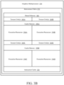
- FIG. 3B shows a graphics multiprocessor 350 according to an additional example.
- the graphics processor includes multiple sets of execution resources 356A-356D, where each set of execution resource includes multiple instruction units, register files, GPGPU cores, and load store units, as illustrated in FIG. 2D and FIG. 3A .
- the execution resources 356A-356D can work in concert with texture unit(s) 360A-360D for texture operations, while sharing an instruction cache 354, and shared memory 362.
- the execution resources 356A-356D can share an instruction cache 354 and shared memory 362, as well as multiple instances of a texture and/or data cache memory 358A-358B.
- the various components can communicate via an interconnect fabric 352 similar to the interconnect fabric 327 of FIG. 3A .
- a parallel processor or GPGPU as described herein is communicatively coupled to host/processor cores to accelerate graphics operations, machine-learning operations, pattern analysis operations, and various general purpose GPU (GPGPU) functions.
- the GPU may be communicatively coupled to the host processor/cores over a bus or other interconnect (e.g., a high speed interconnect such as PCIe or NVLink).
- the GPU may be integrated on the same package or chip as the cores and communicatively coupled to the cores over an internal processor bus/interconnect (i.e., internal to the package or chip).
- the processor cores may allocate work to the GPU in the form of sequences of commands/instructions contained in a work descriptor.
- the GPU then uses dedicated circuitry/logic for efficiently processing these commands/instructions.
- FIG. 4A illustrates an exemplary architecture in which a plurality of GPUs 410-413 are communicatively coupled to a plurality of multi-core processors 405-406 over high-speed links 440-443 (e.g., buses, point-to-point interconnects, etc.).
- the high-speed links 440-443 support a communication throughput of 4GB/s, 30GB/s, 80GB/s or higher, depending on the implementation.
- Various interconnect protocols may be used including, but not limited to, PCIe 4.0 or 5.0 and NVLink 2.0. However, the underlying principles of the invention are not limited to any particular communication protocol or throughput.
- two or more of the GPUs 410-413 are interconnected over high-speed links 444-445, which may be implemented using the same or different protocols/links than those used for high-speed links 440-443.
- two or more of the multi-core processors 405-406 may be connected over high speed link 433 which may be symmetric multi-processor (SMP) buses operating at 20GB/s, 30GB/s, 120GB/s or higher.
- SMP symmetric multi-processor
- each multi-core processor 405-406 is communicatively coupled to a processor memory 401-402, via memory interconnects 430-431, respectively, and each GPU 410-413 is communicatively coupled to GPU memory 420-423 over GPU memory interconnects 450-453, respectively.
- the memory interconnects 430-431 and 450-453 may utilize the same or different memory access technologies.
- the processor memories 401-402 and GPU memories 420-423 may be volatile memories such as dynamic random access memories (DRAMs) (including stacked DRAMs), Graphics DDR SDRAM (GDDR) (e.g., GDDR5, GDDR6), or High Bandwidth Memory (HBM) and/or may be non-volatile memories such as 3D XPoint or Nano-Ram.
- DRAMs dynamic random access memories
- GDDR Graphics DDR SDRAM
- HBM High Bandwidth Memory
- some portion of the memories may be volatile memory and another portion may be non-volatile memory (e.g., using a two-level memory (2LM) hierarchy).
- 2LM two-level memory
- processors 405-406 and GPUs 410-413 may be physically coupled to a particular memory 401-402, 420-423, respectively, a unified memory architecture may be implemented in which the same virtual system address space (also referred to as the "effective address" space) is distributed among all of the various physical memories.
- processor memories 401-402 may each comprise 64GB of the system memory address space
- GPU memories 420-423 may each comprise 32GB of the system memory address space (resulting in a total of 256GB addressable memory in this example).
- FIG. 4B illustrates additional details for an interconnection between a multi-core processor 407 and a graphics acceleration module 446 in accordance with one example.
- the graphics acceleration module 446 may include one or more GPU chips integrated on a line card which is coupled to the processor 407 via the high-speed link 440. Alternatively, the graphics acceleration module 446 may be integrated on the same package or chip as the processor 407.
- the illustrated processor 407 includes a plurality of cores 460A-460D, each with a translation lookaside buffer 461A-461D and one or more caches 462A-462D.
- the cores may include various other components for executing instructions and processing data which are not illustrated to avoid obscuring the underlying principles of the invention (e.g., instruction fetch units, branch prediction units, decoders, execution units, reorder buffers, etc.).
- the caches 462A-462D may comprise level 1 (L1) and level 2 (L2) caches.
- one or more shared caches 426 may be included in the caching hierarchy and shared by sets of the cores 460A-460D.
- processor 407 includes 24 cores, each with its own L1 cache, twelve shared L2 caches, and twelve shared L3 caches. In this example, one of the L2 and L3 caches are shared by two adjacent cores.
- the processor 407 and the graphics accelerator integration module 446 connect with system memory 441, which may include processor memories 401-402
- Coherency is maintained for data and instructions stored in the various caches 462A-462D, 456 and system memory 441 via inter-core communication over a coherence bus 464.
- each cache may have cache coherency logic/circuitry associated therewith to communicate to over the coherence bus 464 in response to detected reads or writes to particular cache lines.
- a cache snooping protocol is implemented over the coherence bus 464 to snoop cache accesses. Cache snooping/coherency techniques are well understood by those of skill in the art and will not be described in detail here to avoid obscuring the underlying principles of the invention.
- proxy circuit 425 which takes part in the cache coherency mechanism on behalf of cache 438 and memories 433-434, N (e.g., sending updates to the cache 438 related to modifications/accesses of cache lines on processor caches 462A-462D, 456 and receiving updates from the cache 438).
- a set of registers 445 store context data for threads executed by the graphics processing engines 431-432, N and a context management circuit 448 manages the thread contexts.
- the context management circuit 448 may perform save and restore operations to save and restore contexts of the various threads during contexts switches (e.g., where a first thread is saved and a second thread is stored so that the second thread can be execute by a graphics processing engine).
- the context management circuit 448 may store current register values to a designated region in memory (e.g., identified by a context pointer). It may then restore the register values when returning to the context.
- an interrupt management circuit 447 receives and processes interrupts received from system devices.
- the accelerator integration circuit acts as a bridge to the system for the graphics acceleration module 446 and provides address translation and system memory cache services.
- the accelerator integration circuit 436 may provide virtualization facilities for the host processor to manage virtualization of the graphics processing engines, interrupts, and memory management.
- any host processor can address these resources directly using an effective address value.
- One function of the accelerator integration circuit 436 is the physical separation of the graphics processing engines 431-432, N so that they appear to the system as independent units.
- one or more graphics memories 433-434, M are coupled to each of the graphics processing engines 431-432, N, respectively.
- the graphics memories 433-434, M store instructions and data being processed by each of the graphics processing engines 431-432, N.
- the graphics memories 433-434, M may be volatile memories such as DRAMs (including stacked DRAMs), GDDR memory (e.g., GDDR5, GDDR6), or HBM, and/or may be non-volatile memories such as 3D XPoint or Nano-Ram.
- biasing techniques are used to ensure that the data stored in graphics memories 433-434, M is data which will be used most frequently by the graphics processing engines 431-432, N and preferably not used by the cores 460A-460D (at least not frequently).
- the biasing mechanism attempts to keep data needed by the cores (and preferably not the graphics processing engines 431-432, N) within the caches 462A-462D, 456 of the cores and system memory 411.
- FIG. 4C illustrates another example in which the accelerator integration circuit 436 is integrated within the processor 407.
- the graphics processing engines 431-432, N communicate directly over the high-speed link 440 to the accelerator integration circuit 436 via interface 437 and interface 435 (which, again, may be utilize any form of bus or interface protocol).
- the accelerator integration circuit 436 may perform the same operations as those described with respect to FIG. 4B , but potentially at a higher throughput given its close proximity to the coherency bus 462 and caches 462A-462D, 426.
- the graphics processing engines 431-432, N may be shared by multiple VM/application partitions.
- the shared models require a system hypervisor to virtualize the graphics processing engines 431-432, N to allow access by each operating system.
- the graphics processing engines 431-432, N are owned by the operating system. In both cases, the operating system can virtualize the graphics processing engines 431-432, N to provide access to each process or application.
- the graphics acceleration module 446 or an individual graphics processing engine 431-432, N selects a process element using a process handle.
- process elements are stored in system memory 411 and are addressable using the effective address to real address translation techniques described herein.
- the process handle may be an implementation-specific value provided to the host process when registering its context with the graphics processing engine 431-432, N (that is, calling system software to add the process element to the process element linked list).
- the lower 16-bits of the process handle may be the offset of the process element within the process element linked list.
- the shared programming models allow for all or a subset of processes from all or a subset of partitions in the system to use a graphics acceleration module 446.
- the system hypervisor 496 owns the graphics acceleration module 446 and makes its function available to all operating systems 495.
- the graphics acceleration module 446 may adhere to the following requirements: 1) An application's job request must be autonomous (that is, the state does not need to be maintained between jobs), or the graphics acceleration module 446 must provide a context save and restore mechanism. 2) An application's job request is guaranteed by the graphics acceleration module 446 to complete in a specified amount of time, including any translation faults, or the graphics acceleration module 446 provides the ability to preempt the processing of the job. 3) The graphics acceleration module 446 must be guaranteed fairness between processes when operating in the directed shared programming model.
- the operating system 495 may verify that the application 480 has registered and been given the authority to use the graphics acceleration module 446. The operating system 495 then calls the hypervisor 496 with the information shown in Table 3. Table 3 - OS to Hypervisor Call Parameters 1 A work descriptor (WD) 2 An Authority Mask Register (AMR) value (potentially masked). 3 An effective address (EA) Context Save/Restore Area Pointer (CSRP) 4 A process ID (PID) and optional thread ID (TID) 5 A virtual address (VA) accelerator utilization record pointer (AURP) 6 The virtual address of the storage segment table pointer (SSTP) 7 A logical interrupt service number (LISN)
- the hypervisor 496 Upon receiving the hypervisor call, the hypervisor 496 verifies that the operating system 495 has registered and been given the authority to use the graphics acceleration module 446. The hypervisor 496 then puts the process element 483 into the process element linked list for the corresponding graphics acceleration module 446 type.
- the process element may include the information shown in Table 4.
- Table 4 - Process Element Information 1 A work descriptor (WD) 2 An Authority Mask Register (AMR) value (potentially masked).
- EA Context Save/Restore Area Pointer
- PID process ID
- TID thread ID
- VA accelerator utilization record pointer
- SSTP storage segment table pointer
- LISN logical interrupt service number
- SR state register
- LPID logical partition ID
- RA real address
- SDR Storage Descriptor Register
- the hypervisor initializes a plurality of accelerator integration slice 490 registers 445.
- one example of the invention employs a unified memory addressable via a common virtual memory address space used to access the physical processor memories 401-402 and GPU memories 420-423.
- operations executed on the GPUs 410-413 utilize the same virtual/effective memory address space to access the processors memories 401-402 and vice versa, thereby simplifying programmability.
- a first portion of the virtual/effective address space is allocated to the processor memory 401, a second portion to the second processor memory 402, a third portion to the GPU memory 420, and so on.
- the entire virtual/effective memory space (sometimes referred to as the effective address space) is thereby distributed across each of the processor memories 401-402 and GPU memories 420-423, allowing any processor or GPU to access any physical memory with a virtual address mapped to that memory.
- bias/coherence management circuitry 494A-494E within one or more of the MMUs 439A-439E ensures cache coherence between the caches of the host processors (e.g., 405) and the GPUs 410-413 and implements biasing techniques indicating the physical memories in which certain types of data should be stored. While multiple instances of bias/coherence management circuitry 494A-494E are illustrated in FIG. 4F , the bias/coherence circuitry may be implemented within the MMU of one or more host processors 405 and/or within the accelerator integration circuit 436.
- GPU-attached memory 420-423 allows GPU-attached memory 420-423 to be mapped as part of system memory, and accessed using shared virtual memory (SVM) technology, but without suffering the typical performance drawbacks associated with full system cache coherence.
- SVM shared virtual memory
- the ability to GPU-attached memory 420-423 to be accessed as system memory without onerous cache coherence overhead provides a beneficial operating environment for GPU offload.
- This arrangement allows the host processor 405 software to setup operands and access computation results, without the overhead of tradition I/O DMA data copies. Such traditional copies involve driver calls, interrupts and memory mapped I/O (MMIO) accesses that are all inefficient relative to simple memory accesses.
- MMIO memory mapped I/O
- the bias table entry associated with each access to the GPU-attached memory 420-423 is accessed prior the actual access to the GPU memory, causing the following operations.
- First, local requests from the GPU 410-413 that find their page in GPU bias are forwarded directly to a corresponding GPU memory 420-423.
- Local requests from the GPU that find their page in host bias are forwarded to the processor 405 (e.g., over a high-speed link as discussed above).
- requests from the processor 405 that find the requested page in host processor bias complete the request like a normal memory read.
- requests directed to a GPU-biased page may be forwarded to the GPU 410-413. The GPU may then transition the page to a host processor bias if it is not currently using the page.
- cache coherency is maintained by temporarily rendering GPU-biased pages uncacheable by the host processor 405.
- the processor 405 may request access from the GPU 410 which may or may not grant access right away, depending on the implementation.
- the processor 405 may request access from the GPU 410 which may or may not grant access right away, depending on the implementation.
- FIG. 5 illustrates a graphics processing pipeline 500, according to an example.
- a graphics processor can implement the illustrated graphics processing pipeline 500.
- the graphics processor can be included within the parallel processing subsystems as described herein, such as the parallel processor 200 of FIG. 2 , which, in one example, is a variant of the parallel processor(s) 112 of FIG. 1 .
- the various parallel processing systems can implement the graphics processing pipeline 500 via one or more instances of the parallel processing unit (e.g., parallel processing unit 202 of FIG. 2 ) as described herein.
- a shader unit e.g., graphics multiprocessor 234 of FIG.
- a vertex processing unit 504 may be configured to perform the functions of one or more of a vertex processing unit 504, a tessellation control processing unit 508, a tessellation evaluation processing unit 512, a geometry processing unit 516, and a fragment/pixel processing unit 524.
- the functions of data assembler 502, primitive assemblers 506, 514, 518, tessellation unit 510, rasterizer 522, and raster operations unit 526 may also be performed by other processing engines within a processing cluster (e.g., processing cluster 214 of FIG. 3 ) and a corresponding partition unit (e.g., partition unit 220A-220N of FIG. 2 ).
- the graphics processing pipeline 500 may also be implemented using dedicated processing units for one or more functions.
- one or more portions of the graphics processing pipeline 500 can be performed by parallel processing logic within a general purpose processor (e.g., CPU). In one example, one or more portions of the graphics processing pipeline 500 can access on-chip memory (e.g., parallel processor memory 222 as in FIG. 2 ) via a memory interface 528, which may be an instance of the memory interface 218 of FIG. 2 .
- a general purpose processor e.g., CPU
- on-chip memory e.g., parallel processor memory 222 as in FIG. 2
- memory interface 528 may be an instance of the memory interface 218 of FIG. 2 .
- the data assembler 502 is a processing unit that collects vertex data for surfaces and primitives. The data assembler 502 then outputs the vertex data, including the vertex attributes, to the vertex processing unit 504.
- the vertex processing unit 504 is a programmable execution unit that executes vertex shader programs, lighting and transforming vertex data as specified by the vertex shader programs.
- the vertex processing unit 504 reads data that is stored in cache, local or system memory for use in processing the vertex data and may be programmed to transform the vertex data from an object-based coordinate representation to a world space coordinate space or a normalized device coordinate space.
- a first instance of a primitive assembler 506 receives vertex attributes from the vertex processing unit 50.
- the primitive assembler 506 readings stored vertex attributes as needed and constructs graphics primitives for processing by tessellation control processing unit 508.
- the graphics primitives include triangles, line segments, points, patches, and so forth, as supported by various graphics processing application programming interfaces (APIs).
- the tessellation control processing unit 508 treats the input vertices as control points for a geometric patch.
- the control points are transformed from an input representation from the patch (e.g., the patch's bases) to a representation that is suitable for use in surface evaluation by the tessellation evaluation processing unit 512.
- the tessellation control processing unit 508 can also compute tessellation factors for edges of geometric patches.
- a tessellation factor applies to a single edge and quantifies a view-dependent level of detail associated with the edge.
- a tessellation unit 510 is configured to receive the tessellation factors for edges of a patch and to tessellate the patch into multiple geometric primitives such as line, triangle, or quadrilateral primitives, which are transmitted to a tessellation evaluation processing unit 512.
- the tessellation evaluation processing unit 512 operates on parameterized coordinates of the subdivided patch to generate a surface representation and vertex attributes for each vertex associated with the geometric primitives.
- a learning model can be applied to the network to train the network to perform specific tasks.
- the learning model describes how to adjust the weights within the model to reduce the output error of the network.
- Backpropagation of errors is a common method used to train neural networks. An input vector is presented to the network for processing. The output of the network is compared to the desired output using a loss function and an error value is calculated for each of the neurons in the output layer. The error values are then propagated backwards until each neuron has an associated error value which roughly represents its contribution to the original output. The network can then learn from those errors using an algorithm, such as the stochastic gradient descent algorithm, to update the weights of the of the neural network.
- an algorithm such as the stochastic gradient descent algorithm
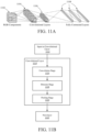
- FIG. 11A-B illustrate an exemplary convolutional neural network.
- FIG. 11A illustrates various layers within a CNN.
- an exemplary CNN used to model image processing can receive input 1102 describing the red, green, and blue (RGB) components of an input image.
- the input 1102 can be processed by multiple convolutional layers (e.g., convolutional layer 1104, convolutional layer 1106).
- the output from the multiple convolutional layers may optionally be processed by a set of fully connected layers 1108.
- Neurons in a fully connected layer have full connections to all activations in the previous layer, as previously described for a feedforward network.
- the output from the fully connected layers 1108 can be used to generate an output result from the network.
- the activations within the fully connected layers 1108 can be computed using matrix multiplication instead of convolution. Not all CNN implementations are make use of fully connected layers 1108.
- the convolutional layer 1106 can generate output for the CNN.
- the initial weights may be chosen randomly or by pre-training using a deep belief network.
- the training cycle then be performed in either a supervised or unsupervised manner.
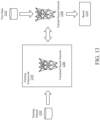
- Supervised learning is a learning method in which training is performed as a mediated operation, such as when the training dataset 1302 includes input paired with the desired output for the input, or where the training dataset includes input having known output and the output of the neural network is manually graded.
- the network processes the inputs and compares the resulting outputs against a set of expected or desired outputs. Errors are then propagated back through the system.
- the training framework 1304 can adjust to adjust the weights that control the untrained neural network 1306.
- the training framework 1304 can provide tools to monitor how well the untrained neural network 1306 is converging towards a model suitable to generating correct answers based on known input data.
- the training process occurs repeatedly as the weights of the network are adjusted to refine the output generated by the neural network.
- the training process can continue until the neural network reaches a statistically desired accuracy associated with a trained neural net 1308.
- the trained neural network 1308 can then be deployed to implement any number of machine learning operations.
- Unsupervised learning is a learning method in which the network attempts to train itself using unlabeled data.
- the training dataset 1302 will include input data without any associated output data.
- the untrained neural network 1306 can learn groupings within the unlabeled input and can determine how individual inputs are related to the overall dataset.
- Unsupervised training can be used to generate a self-organizing map, which is a type of trained neural network 1307 capable of performing operations useful in reducing the dimensionality of data.
- Unsupervised training can also be used to perform anomaly detection, which allows the identification of data points in an input dataset that deviate from the normal patterns of the data.
- Semi-supervised learning is a technique in which in the training dataset 1302 includes a mix of labeled and unlabeled data of the same distribution.
- Incremental learning is a variant of supervised learning in which input data is continuously used to further train the model. Incremental learning enables the trained neural network 1308 to adapt to the new data 1312 without forgetting the knowledge instilled within the network during initial training.
- the training process for particularly deep neural networks may be too computationally intensive for a single compute node.
- a distributed network of computational nodes can be used to accelerate the training process.
- model parallelism 1402 different computational nodes in a distributed system can perform training computations for different parts of a single network. For example, each layer of a neural network can be trained by a different processing node of the distributed system.
- the benefits of model parallelism include the ability to scale to particularly large models. Splitting the computations associated with different layers of the neural network enables the training of very large neural networks in which the weights of all layers would not fit into the memory of a single computational node. In some instances, model parallelism can be particularly useful in performing unsupervised training of large neural networks.
- data parallelism 1404 the different nodes of the distributed network have a complete instance of the model and each node receives a different portion of the data. The results from the different nodes are then combined. While different approaches to data parallelism are possible, data parallel training approaches all require a technique of combining results and synchronizing the model parameters between each node. Exemplary approaches to combining data include parameter averaging and update based data parallelism. Parameter averaging trains each node on a subset of the training data and sets the global parameters (e.g., weights, biases) to the average of the parameters from each node. Parameter averaging uses a central parameter server that maintains the parameter data.
- parameter averaging trains each node on a subset of the training data and sets the global parameters (e.g., weights, biases) to the average of the parameters from each node. Parameter averaging uses a central parameter server that maintains the parameter data.
- Update based data parallelism is similar to parameter averaging except that instead of transferring parameters from the nodes to the parameter server, the updates to the model are transferred. Additionally, update based data parallelism can be performed in a decentralized manner, where the updates are compressed and transferred between nodes.
- Combined model and data parallelism 1406 can be implemented, for example, in a distributed system in which each computational node includes multiple GPUs. Each node can have a complete instance of the model with separate GPUs within each node are used to train different portions of the model.
- Distributed training has increased overhead relative to training on a single machine.
- the parallel processors and GPGPUs described herein can each implement various techniques to reduce the overhead of distributed training, including techniques to enable high bandwidth GPU-to-GPU data transfer and accelerated remote data synchronization.
- ASR automatic speech recognition
- HMMs hidden Markov models
- GMMs Gaussian mixture models
- the multi-core processor 1508 can include control logic to assist with sequencing and synchronization of data transfers and shared memory operations performed by the media processor 1502 and the vision processor 1504.
- the multi-core processor 1508 can also function as an application processor to execute software applications that can make use of the inferencing compute capability of the GPGPU 1506. For example, at least a portion of the navigation and driving logic can be implemented in software executing on the multi-core processor 1508. Such software can directly issue computational workloads to the GPGPU 1506 or the computational workloads can be issued to the multi-core processor 1508, which can offload at least a portion of those operations to the GPGPU 1506.
- FIG. 21-34 illustrate alternative systems and graphics processing hardware that can implement any and all of the techniques described above.
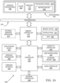
- FIG. 16 is a block diagram of a processing system 1600, according to an example.
- the system 1600 includes one or more processors 1602 and one or more graphics processors 1608, and may be a single processor desktop system, a multiprocessor workstation system, or a server system having a large number of processors 1602 or processor cores 1607.
- the system 1600 is a processing platform incorporated within a system-on-a-chip (SoC) integrated circuit for use in mobile, handheld, or embedded devices.
- SoC system-on-a-chip
- System 1600 can include, or be incorporated within a server-based gaming platform, a game console, including a game and media console, a mobile gaming console, a handheld game console, or an online game console.
- system 1600 is a mobile phone, smart phone, tablet computing device or mobile Internet device.
- Data processing system 1600 can also include, couple with, or be integrated within a wearable device, such as a smart watch wearable device, smart eyewear device, augmented reality device, or virtual reality device.
- data processing system 1600 is a television or set top box device having one or more processors 1602 and a graphical interface generated by one or more graphics processors 1608.
- the processor 1602 includes cache memory 1604. Depending on the architecture, the processor 1602 can have a single internal cache or multiple levels of internal cache. In some examples, the cache memory is shared among various components of the processor 1602. In some examples, the processor 1602 also uses an external cache (e.g., a Level-3 (L3) cache or Last Level Cache (LLC)) (not shown), which may be shared among processor cores 1607 using known cache coherency techniques.
- L3 cache Level-3
- LLC Last Level Cache
- a register file 1606 is additionally included in processor 1602 which may include different types of registers for storing different types of data (e.g., integer registers, floating point registers, status registers, and an instruction pointer register). Some registers may be general-purpose registers, while other registers may be specific to the design of the processor 1602.
- processor 1602 is coupled with a processor bus 1610 to transmit communication signals such as address, data, or control signals between processor 1602 and other components in system 1600.
- the system 1600 uses an exemplary 'hub' system architecture, including a memory controller hub 1616 and an Input Output (I/O) controller hub 1630.
- a memory controller hub 1616 facilitates communication between a memory device and other components of system 1600, while an I/O Controller Hub (ICH) 1630 provides connections to I/O devices via a local I/O bus.
- ICH I/O Controller Hub
- the logic of the memory controller hub 1616 is integrated within the processor.
- Memory device 1620 can be a dynamic random access memory (DRAM) device, a static random access memory (SRAM) device, flash memory device, phase-change memory device, or some other memory device having suitable performance to serve as process memory.
- the memory device 1620 can operate as system memory for the system 1600, to store data 1622 and instructions 1621 for use when the one or more processors 1602 executes an application or process.
- Memory controller hub 1616 also couples with an optional external graphics processor 1612, which may communicate with the one or more graphics processors 1608 in processors 1602 to perform graphics and media operations.
- ICH 1630 enables peripherals to connect to memory device 1620 and processor 1602 via a high-speed I/O bus.
- the I/O peripherals include, but are not limited to, an audio controller 1646, a firmware interface 1628, a wireless transceiver 1626 (e.g., Wi-Fi, Bluetooth), a data storage device 1624 (e.g., hard disk drive, flash memory, etc.), and a legacy I/O controller 1640 for coupling legacy (e.g., Personal System 2 (PS/2)) devices to the system.
- PS/2 Personal System 2
- One or more Universal Serial Bus (USB) controllers 1642 connect input devices, such as keyboard and mouse 1644 combinations.
- a network controller 1634 may also couple with ICH 1630.
- a high-performance network controller (not shown) couples with processor bus 1610. It will be appreciated that the system 1600 shown is exemplary and not limiting, as other types of data processing systems that are differently configured may also be used.
- the I/O controller hub 1630 may be integrated within the one or more processor 1602, or the memory controller hub 1616 and I/O controller hub 1630 may be integrated into a discreet external graphics processor, such as the external graphics processor 1612.
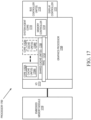
- FIG. 17 is a block diagram of an example of a processor 1700 having one or more processor cores 1702A-1702N, an integrated memory controller 1714, and an integrated graphics processor 1708. Those elements of FIG. 17 having the same reference numbers (or names) as the elements of any other figure herein can operate or function in any manner similar to that described elsewhere herein, but are not limited to such.
- Processor 1700 can include additional cores up to and including additional core 1702N represented by the dashed lined boxes.
- Each of processor cores 1702A-1702N includes one or more internal cache units 1704A-1704N. In some examples each processor core also has access to one or more shared cached units 1706.
- the internal cache units 1704A-1704N and shared cache units 1706 represent a cache memory hierarchy within the processor 1700.
- the cache memory hierarchy may include at least one level of instruction and data cache within each processor core and one or more levels of shared mid-level cache, such as a Level 2 (L2), Level 3 (L3), Level 4 (L4), or other levels of cache, where the highest level of cache before external memory is classified as the LLC.
- cache coherency logic maintains coherency between the various cache units 1706 and 1704A-1704N.
- processor 1700 may also include a set of one or more bus controller units 1716 and a system agent core 1710.
- the one or more bus controller units 1716 manage a set of peripheral buses, such as one or more Peripheral Component Interconnect buses (e.g., PCI, PCI Express).
- System agent core 1710 provides management functionality for the various processor components.
- system agent core 1710 includes one or more integrated memory controllers 1714 to manage access to various external memory devices (not shown).
- one or more of the processor cores 1702A-1702N include support for simultaneous multi-threading.
- the system agent core 1710 includes components for coordinating and operating processor cores 1702A-1702N during multi-threaded processing.
- System agent core 1710 may additionally include a power control unit (PCU), which includes logic and components to regulate the power state of processor cores 1702A-1702N and graphics processor 1708.
- PCU power control unit
- processor 1700 additionally includes graphics processor 1708 to execute graphics processing operations.
- the graphics processor 1708 couples with the set of shared cache units 1706, and the system agent core 1710, including the one or more integrated memory controllers 1714.
- a display controller 1711 is coupled with the graphics processor 1708 to drive graphics processor output to one or more coupled displays.
- display controller 1711 may be a separate module coupled with the graphics processor via at least one interconnect, or may be integrated within the graphics processor 1708 or system agent core 1710.
- the exemplary I/O link 1713 represents at least one of multiple varieties of I/O interconnects, including an on-package I/O interconnect which facilitates communication between various processor components and a high-performance embedded memory module 1718, such as an eDRAM module.
- a high-performance embedded memory module 1718 such as an eDRAM module.
- each of the processor cores 1702A-1702N and graphics processor 1708 use embedded memory modules 1718 as a shared Last Level Cache.
- processor cores 1702A-1702N are homogenous cores executing the same instruction set architecture.
- processor cores 1702A-1702N are heterogeneous in terms of instruction set architecture (ISA), where one or more of processor cores 1702A-1702N execute a first instruction set, while at least one of the other cores executes a subset of the first instruction set or a different instruction set.
- processor cores 1702A-1702N are heterogeneous in terms of microarchitecture, where one or more cores having a relatively higher power consumption couple with one or more power cores having a lower power consumption.
- processor 1700 can be implemented on one or more chips or as an SoC integrated circuit having the illustrated components, in addition to other components.
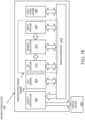
- FIG. 18 is a block diagram of a graphics processor 1800, which may be a discrete graphics processing unit, or may be a graphics processor integrated with a plurality of processing cores.
- the graphics processor communicates via a memory mapped I/O interface to registers on the graphics processor and with commands placed into the processor memory.
- graphics processor 1800 includes a memory interface 1814 to access memory.
- Memory interface 1814 can be an interface to local memory, one or more internal caches, one or more shared external caches, and/or to system memory.
- graphics processor 1800 includes a block image transfer (BLIT) engine 1804 to perform two-dimensional (2D) rasterizer operations including, for example, bit-boundary block transfers.
- 2D graphics operations are performed using one or more components of graphics processing engine (GPE) 1810.
- GPE 1810 is a compute engine for performing graphics operations, including three-dimensional (3D) graphics operations and media operations.
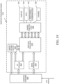
- graphics processor 2000 includes scalable thread execution resources featuring modular cores 2080A-2080N (sometimes referred to as core slices), each having multiple sub-cores 2050A-550N, 2060A-2060N (sometimes referred to as core sub-slices).
- graphics processor 2000 can have any number of graphics cores 2080A through 2080N.
- graphics processor 2000 includes a graphics core 2080A having at least a first sub-core 2050A and a second sub-core 2060A.
- the graphics processor is a low power processor with a single sub-core (e.g., 2050A).
- graphics processor 2000 includes multiple graphics cores 2080A-2080N, each including a set of first sub-cores 2050A-2050N and a set of second sub-cores 2060A-2060N.
- Each sub-core in the set of first sub-cores 2050A-2050N includes at least a first set of execution units 2052A-2052N and media/texture samplers 2054A-2054N.
- Each sub-core in the set of second sub-cores 2060A-2060N includes at least a second set of execution units 2062A-2062N and samplers 2064A-2064N.
- each sub-core 2050A-2050N, 2060A-2060N shares a set of shared resources 2070A-2070N.
- the shared resources include shared cache memory and pixel operation logic. Other shared resources may also be included in the various examples of the graphics processor.
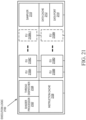
- FIG. 21 illustrates thread execution logic 2100 including an array of processing elements employed in some examples of a GPE. Elements of FIG. 21 having the same reference numbers (or names) as the elements of any other figure herein can operate or function in any manner similar to that described elsewhere herein, but are not limited to such.
- thread execution logic 2100 includes a shader processor 2102, a thread dispatcher 2104, instruction cache 2106, a scalable execution unit array including a plurality of execution units 2108A-2108N, a sampler 2110, a data cache 2112, and a data port 2114.
- the scalable execution unit array can dynamically scale by enabling or disabling one or more execution units (e.g., any of execution unit 2108A, 2108B, 2108C, 2108D, through 2108N-1 and 2108N) based on the computational requirements of a workload.
- the included components are interconnected via an interconnect fabric that links to each of the components.
- thread execution logic 2100 includes one or more connections to memory, such as system memory or cache memory, through one or more of instruction cache 2106, data port 2114, sampler 2110, and execution units 2108A-2108N.
- each execution unit e.g. 2108A
- each execution unit is a stand-alone programmable general purpose computational unit that is capable of executing multiple simultaneous hardware threads while processing multiple data elements in parallel for each thread.
- the array of execution units 2108A-2108N is scalable to include any number individual execution units.
- the execution units 2108A-2108N are primarily used to execute shader programs.
- a shader processor 2102 can process the various shader programs and dispatch execution threads associated with the shader programs via a thread dispatcher 2104.
- the thread dispatcher includes logic to arbitrate thread initiation requests from the graphics and media pipelines and instantiate the requested threads on one or more execution unit in the execution units 2108A-2108N.
- the geometry pipeline e.g., 2036 of FIG. 20
- thread dispatcher 2104 can also process runtime thread spawning requests from the executing shader programs.
- the execution units 2108A-2108N support an instruction set that includes native support for many standard 3D graphics shader instructions, such that shader programs from graphics libraries (e.g., Direct 3D and OpenGL) are executed with a minimal translation.
- the execution units support vertex and geometry processing (e.g., vertex programs, geometry programs, vertex shaders), pixel processing (e.g., pixel shaders, fragment shaders) and general-purpose processing (e.g., compute and media shaders).
- Each of the execution units 2108A-2108N is capable of multi-issue single instruction multiple data (SIMD) execution and multi-threaded operation enables an efficient execution environment in the face of higher latency memory accesses.
- SIMD single instruction multiple data
- Each execution unit in execution units 2108A-2108N operates on arrays of data elements.
- the number of data elements is the "execution size," or the number of channels for the instruction.
- An execution channel is a logical unit of execution for data element access, masking, and flow control within instructions.
- the number of channels may be independent of the number of physical Arithmetic Logic Units (ALUs) or Floating Point Units (FPUs) for a particular graphics processor.
- ALUs Arithmetic Logic Units
- FPUs Floating Point Units
- execution units 2108A-2108N support integer and floating-point data types.
- the execution unit instruction set includes SIMD instructions.
- the various data elements can be stored as a packed data type in a register and the execution unit will process the various elements based on the data size of the elements. For example, when operating on a 256-bit wide vector, the 256 bits of the vector are stored in a register and the execution unit operates on the vector as four separate 64-bit packed data elements (Quad-Word (QW) size data elements), eight separate 32-bit packed data elements (Double Word (DW) size data elements), sixteen separate 16-bit packed data elements (Word (W) size data elements), or thirty-two separate 8-bit data elements (byte (B) size data elements).
- QW Quad-Word
- DW Double Word
- W 16-bit packed data elements
- B thirty-two separate 8-bit data elements
- One or more internal instruction caches are included in the thread execution logic 2100 to cache thread instructions for the execution units.
- one or more data caches are included to cache thread data during thread execution.
- a sampler 2110 is included to provide texture sampling for 3D operations and media sampling for media operations.
- sampler 2110 includes specialized texture or media sampling functionality to process texture or media data during the sampling process before providing the sampled data to an execution unit.
- pixel processor logic within the shader processor 2102 is invoked to further compute output information and cause results to be written to output surfaces (e.g., color buffers, depth buffers, stencil buffers, etc.).
- output surfaces e.g., color buffers, depth buffers, stencil buffers, etc.
- a pixel shader or fragment shader calculates the values of the various vertex attributes that are to be interpolated across the rasterized object.
- pixel processor logic within the shader processor 2102 then executes an application programming interface (API)-supplied pixel or fragment shader program.
- API application programming interface
- the shader processor 2102 dispatches threads to an execution unit (e.g., 2108A) via thread dispatcher 2104.
- pixel shader 2102 uses texture sampling logic in the sampler 2110 to access texture data in texture maps stored in memory. Arithmetic operations on the texture data and the input geometry data compute pixel color data for each geometric fragment, or discards one or more pixels from further processing.
- the data port 2114 provides a memory access mechanism for the thread execution logic 2100 output processed data to memory for processing on a graphics processor output pipeline.
- the data port 2114 includes or couples to one or more cache memories (e.g., data cache 2112) to cache data for memory access via the data port.
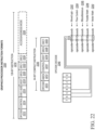
- FIG. 22 is a block diagram illustrating a graphics processor instruction formats 2200 according to some examples.
- the graphics processor execution units support an instruction set having instructions in multiple formats.
- the solid lined boxes illustrate the components that are generally included in an execution unit instruction, while the dashed lines include components that are optional or that are only included in a sub-set of the instructions.
- instruction format 2200 described and illustrated are macro-instructions, in that they are instructions supplied to the execution unit, as opposed to micro-operations resulting from instruction decode once the instruction is processed.
- the graphics processor execution units natively support instructions in a 128-bit instruction format 2210.
- a 64-bit compacted instruction format 2230 is available for some instructions based on the selected instruction, instruction options, and number of operands.
- the native 128-bit instruction format 710 provides access to all instruction options, while some options and operations are restricted in the 64-bit format 2230.
- the native instructions available in the 64-bit format 2230 vary by example.
- the instruction is compacted in part using a set of index values in an index field 2213.
- the execution unit hardware references a set of compaction tables based on the index values and uses the compaction table outputs to reconstruct a native instruction in the 128-bit instruction format 2210.
- the 128-bit instruction format 2210 includes an access/address mode field 2226 specifying, for example, whether direct register addressing mode or indirect register addressing mode is used. When direct register addressing mode is used, the register address of one or more operands is directly provided by bits in the instruction.
- the 128-bit instruction format 2210 includes an access/address mode field 2226, which specifies an address mode and/or an access mode for the instruction.
- the access mode is used to define a data access alignment for the instruction.
- Some examples support access modes including a 16-byte aligned access mode and a 1-byte aligned access mode, where the byte alignment of the access mode determines the access alignment of the instruction operands. For example, when in a first mode, the instruction may use byte-aligned addressing for source and destination operands and when in a second mode, the instruction may use 16-byte-aligned addressing for all source and destination operands.
- the address mode portion of the access/address mode field 2226 determines whether the instruction is to use direct or indirect addressing.
- direct register addressing mode bits in the instruction directly provide the register address of one or more operands.
- indirect register addressing mode the register address of one or more operands may be computed based on an address register value and an address immediate field in the instruction.
- instructions are grouped based on opcode 2212 bit-fields to simplify Opcode decode 2240.
- bits 4, 5, and 6 allow the execution unit to determine the type of opcode.
- the precise opcode grouping shown is merely an example.
- a move and logic opcode group 2242 includes data movement and logic instructions (e.g., move (mov), compare (cmp)).
- move and logic opcode group 2242 shares the five most significant bits (MSB), where move (mov) instructions are in the form of 0000xxxxb and logic instructions are in the form of 0001xxxxb.
- a flow control instruction group 2244 (e.g., call, jump (jmp)) includes instructions in the form of 0010xxxxb (e.g., 0x20).
- a miscellaneous instruction group 2246 includes a mix of instructions, including synchronization instructions (e.g., wait, send) in the form of 0011xxxxb (e.g., 0x30).
- a parallel math instruction group 2248 includes component-wise arithmetic instructions (e.g., add, multiply (mul)) in the form of 0100xxxxb (e.g., 0x40). The parallel math group 2248 performs the arithmetic operations in parallel across data channels.
- the vector math group 2250 includes arithmetic instructions (e.g., dp4) in the form of 0101xxxxb (e.g., 0x50).
- the vector math group performs arithmetic such as dot product calculations on vector operands.
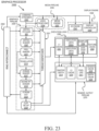
- FIG. 23 is a block diagram of another example of a graphics processor 2300. Elements of FIG. 23 having the same reference numbers (or names) as the elements of any other figure herein can operate or function in any manner similar to that described elsewhere herein, but are not limited to such.
- graphics processor 2300 includes a graphics pipeline 2320, a media pipeline 2330, a display engine 2340, thread execution logic 2350, and a render output pipeline 2370.
- graphics processor 2300 is a graphics processor within a multi-core processing system that includes one or more general purpose processing cores. The graphics processor is controlled by register writes to one or more control registers (not shown) or via commands issued to graphics processor 2300 via a ring interconnect 2302.
- ring interconnect 2302 couples graphics processor 2300 to other processing components, such as other graphics processors or general-purpose processors. Commands from ring interconnect 2302 are interpreted by a command streamer 2303, which supplies instructions to individual components of graphics pipeline 2320 or media pipeline 2330.
- command streamer 2303 directs the operation of a vertex fetcher 2305 that reads vertex data from memory and executes vertex-processing commands provided by command streamer 2303.
- vertex fetcher 2305 provides vertex data to a vertex shader 2307, which performs coordinate space transformation and lighting operations to each vertex.
- vertex fetcher 2305 and vertex shader 2307 execute vertex-processing instructions by dispatching execution threads to execution units 2352A-2352B via a thread dispatcher 2331.
- execution units 2352A-2352B are an array of vector processors having an instruction set for performing graphics and media operations. In some examples, execution units 2352A-2352B have an attached L1 cache 2351 that is specific for each array or shared between the arrays.
- the cache can be configured as a data cache, an instruction cache, or a single cache that is partitioned to contain data and instructions in different partitions.
- graphics pipeline 2320 includes tessellation components to perform hardware-accelerated tessellation of 3D objects.
- a programmable hull shader 811 configures the tessellation operations.
- a programmable domain shader 817 provides back-end evaluation of tessellation output.
- a tessellator 2313 operates at the direction of hull shader 2311 and contains special purpose logic to generate a set of detailed geometric objects based on a coarse geometric model that is provided as input to graphics pipeline 2320.
- tessellation components e.g., hull shader 2311, tessellator 2313, and domain shader 2317
- complete geometric objects can be processed by a geometry shader 2319 via one or more threads dispatched to execution units 2352A-2352B, or can proceed directly to the clipper 2329.
- the geometry shader operates on entire geometric objects, rather than vertices or patches of vertices as in previous stages of the graphics pipeline. If the tessellation is disabled the geometry shader 2319 receives input from the vertex shader 2307. In some examples, geometry shader 2319 is programmable by a geometry shader program to perform geometry tessellation if the tessellation units are disabled.
- graphics pipeline 2320 and media pipeline 2330 are configurable to perform operations based on multiple graphics and media programming interfaces and are not specific to any one application programming interface (API).
- driver software for the graphics processor translates API calls that are specific to a particular graphics or media library into commands that can be processed by the graphics processor.
- support is provided for the Open Graphics Library (OpenGL), Open Computing Language (OpenCL), and/or Vulkan graphics and compute API, all from the Khronos Group.
- support may also be provided for the Direct3D library from the Microsoft Corporation.
- a combination of these libraries may be supported.
- Support may also be provided for the Open Source Computer Vision Library (OpenCV).
- OpenCV Open Source Computer Vision Library
- a future API with a compatible 3D pipeline would also be supported if a mapping can be made from the pipeline of the future API to the pipeline of the graphics processor.
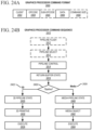
- client 2402 specifies the client unit of the graphics device that processes the command data.
- a graphics processor command parser examines the client field of each command to condition the further processing of the command and route the command data to the appropriate client unit.
- the graphics processor client units include a memory interface unit, a render unit, a 2D unit, a 3D unit, and a media unit. Each client unit has a corresponding processing pipeline that processes the commands.
- the client unit reads the opcode 2404 and, if present, sub-opcode 2405 to determine the operation to perform.
- the client unit performs the command using information in data field 2406.
- an explicit command size 2408 is expected to specify the size of the command.
- the command parser automatically determines the size of at least some of the commands based on the command opcode. In some examples commands are aligned via multiples of a double word.
- FIG. 24B shows an exemplary graphics processor command sequence 2410.
- software or firmware of a data processing system that features an example of a graphics processor uses a version of the command sequence shown to set up, execute, and terminate a set of graphics operations.
- a sample command sequence is shown and described for purposes of example only as examples are not limited to these specific commands or to this command sequence.
- the commands may be issued as batch of commands in a command sequence, such that the graphics processor will process the sequence of commands in at least partially concurrence.
- the graphics processor command sequence 2410 may begin with a pipeline flush command 2412 to cause any active graphics pipeline to complete the currently pending commands for the pipeline.
- the 3D pipeline 2422 and the media pipeline 2424 do not operate concurrently.
- the pipeline flush is performed to cause the active graphics pipeline to complete any pending commands.
- the command parser for the graphics processor will pause command processing until the active drawing engines complete pending operations and the relevant read caches are invalidated.
- any data in the render cache that is marked 'dirty' can be flushed to memory.
- pipeline flush command 2412 can be used for pipeline synchronization or before placing the graphics processor into a low power state.
- a pipeline select command 2413 is used when a command sequence requires the graphics processor to explicitly switch between pipelines. In some examples, a pipeline select command 2413 is required only once within an execution context before issuing pipeline commands unless the context is to issue commands for both pipelines. In some examples, a pipeline flush command 2412 is required immediately before a pipeline switch via the pipeline select command 2413.
- a pipeline control command 2414 configures a graphics pipeline for operation and is used to program the 3D pipeline 2422 and the media pipeline 2424. In some examples, pipeline control command 2414 configures the pipeline state for the active pipeline. In one example, the pipeline control command 2414 is used for pipeline synchronization and to clear data from one or more cache memories within the active pipeline before processing a batch of commands.
- the remaining commands in the command sequence differ based on the active pipeline for operations. Based on a pipeline determination 2420, the command sequence is tailored to the 3D pipeline 2422 beginning with the 3D pipeline state 2430 or the media pipeline 2424 beginning at the media pipeline state 2440.
- the commands to configure the 3D pipeline state 2430 include 3D state setting commands for vertex buffer state, vertex element state, constant color state, depth buffer state, and other state variables that are to be configured before 3D primitive commands are processed. The values of these commands are determined at least in part based on the particular 3D API in use. In some examples, 3D pipeline state 2430 commands are also able to selectively disable or bypass certain pipeline elements if those elements will not be used.
- 3D primitive 2432 command is used to submit 3D primitives to be processed by the 3D pipeline. Commands and associated parameters that are passed to the graphics processor via the 3D primitive 2432 command are forwarded to the vertex fetch function in the graphics pipeline.
- the vertex fetch function uses the 3D primitive 2432 command data to generate vertex data structures. The vertex data structures are stored in one or more return buffers.
- 3D primitive 2432 command is used to perform vertex operations on 3D primitives via vertex shaders. To process vertex shaders, 3D pipeline 2422 dispatches shader execution threads to graphics processor execution units.
- the graphics processor command sequence 2410 follows the media pipeline 2424 path when performing media operations.
- the specific use and manner of programming for the media pipeline 2424 depends on the media or compute operations to be performed. Specific media decode operations may be offloaded to the media pipeline during media decode.
- the media pipeline can also be bypassed and media decode can be performed in whole or in part using resources provided by one or more general purpose processing cores.
- the media pipeline also includes elements for general-purpose graphics processor unit (GPGPU) operations, where the graphics processor is used to perform SIMD vector operations using computational shader programs that are not explicitly related to the rendering of graphics primitives.
- GPGPU general-purpose graphics processor unit
- media pipeline 2424 is configured in a similar manner as the 3D pipeline 2422.
- a set of commands to configure the media pipeline state 2440 are dispatched or placed into a command queue before the media object commands 2442.
- the commands for the media pipeline state 2440 include data to configure the media pipeline elements that will be used to process the media objects. This includes data to configure the video decode and video encode logic within the media pipeline, such as encode or decode format.
- commands for the media pipeline state 2440 enable support the use of one or more pointers to "indirect" state elements that contain a batch of state settings.
- media object commands 2442 supply pointers to media objects for processing by the media pipeline.
- the media objects include memory buffers containing video data to be processed.
- all media pipeline states must be valid before issuing a media object command 2442.
- the media pipeline 2424 is triggered via an execute command 2444 or an equivalent execute event (e.g., register write).
- Output from media pipeline 2424 may then be post processed by operations provided by the 3D pipeline 2422 or the media pipeline 2424.
- GPGPU operations are configured and executed in a similar manner as media operations.
- FIG. 25 illustrates exemplary graphics software architecture for a data processing system 2500 according to some examples.
- software architecture includes a 3D graphics application 2510, an operating system 2520, and at least one processor 2530.
- processor 2530 includes a graphics processor 2532 and one or more general-purpose processor core(s) 2534.
- the graphics application 2510 and operating system 2520 each execute in the system memory 2550 of the data processing system.
- operating system 2520 is a Microsoft ® Windows ® operating system from the Microsoft Corporation, a proprietary UNIX-like operating system, or an open source UNIX-like operating system using a variant of the Linux kernel.
- the operating system 2520 can support a graphics API 2522 such as the Direct3D API, the OpenGL API, or the Vulkan API.
- the operating system 2520 uses a front-end shader compiler 2524 to compile any shader instructions 2512 in HLSL into a lower-level shader language.
- the compilation may be a just-in-time (JIT) compilation or the application can perform shader pre-compilation.
- high-level shaders are compiled into low-level shaders during the compilation of the 3D graphics application 2510.
- the shader instructions 2512 are provided in an intermediate form, such as a version of the Standard Portable Intermediate Representation (SPIR) used by the Vulkan API.
- SPIR Standard Portable Intermediate Representation
- user mode graphics driver 2526 contains a back-end shader compiler 2527 to convert the shader instructions 2512 into a hardware specific representation.
- shader instructions 2512 in the GLSL high-level language are passed to a user mode graphics driver 2526 for compilation.
- user mode graphics driver 2526 uses operating system kernel mode functions 2528 to communicate with a kernel mode graphics driver 2529.
- kernel mode graphics driver 2529 communicates with graphics processor 2532 to dispatch commands and instructions.
- FIG. 26 is a block diagram illustrating an IP core development system 2600 that may be used to manufacture an integrated circuit to perform operations according to an example.
- the IP core development system 2600 may be used to generate modular, reusable designs that can be incorporated into a larger design or used to construct an entire integrated circuit (e.g., an SOC integrated circuit).
- a design facility 2630 can generate a software simulation 2610 of an IP core design in a high level programming language (e.g., C/C++).
- the software simulation 2610 can be used to design, test, and verify the behavior of the IP core using a simulation model 2612.
- the simulation model 2612 may include functional, behavioral, and/or timing simulations.
- a register transfer level (RTL) design 2615 can then be created or synthesized from the simulation model 2612.
- the RTL design 2615 is an abstraction of the behavior of the integrated circuit that models the flow of digital signals between hardware registers, including the associated logic performed using the modeled digital signals.
- lower-level designs at the logic level or transistor level may also be created, designed, or synthesized. Thus, the particular details of the initial design and simulation may vary.
- the RTL design 2615 or equivalent may be further synthesized by the design facility into a hardware model 2620, which may be in a hardware description language (HDL), or some other representation of physical design data.
- the HDL may be further simulated or tested to verify the IP core design.
- the IP core design can be stored for delivery to a 3 rd party fabrication facility 2665 using non-volatile memory 2640 (e.g., hard disk, flash memory, or any non-volatile storage medium).
- the IP core design may be transmitted (e.g., via the Internet) over a wired connection 2650 or wireless connection 2660.
- the fabrication facility 2665 may then fabricate an integrated circuit that is based at least in part on the IP core design.
- the fabricated integrated circuit can be configured to perform operations in accordance with at least one example described herein.
- FIGs. 27-29 illustrated exemplary integrated circuits and associated graphics processors that may be fabricated using one or more IP cores, according to various examples described herein. In addition to what is illustrated, other logic and circuits may be included, including additional graphics processors/cores, peripheral interface controllers, or general purpose processor cores.
- FIG. 27 is a block diagram illustrating an exemplary system on a chip integrated circuit 2700 that may be fabricated using one or more IP cores, according to an example.
- Exemplary integrated circuit 2700 includes one or more application processor(s) 2705 (e.g., CPUs), at least one graphics processor 2710, and may additionally include an image processor 2715 and/or a video processor 2720, any of which may be a modular IP core from the same or multiple different design facilities.
- Integrated circuit 2700 includes peripheral or bus logic including a USB controller 2725, UART controller 2730, an SPI/SDIO controller 2735, and an I 2 S/I 2 C controller 2740.
- FIG. 29 is a block diagram illustrating an additional exemplary graphics processor 2910 of a system on a chip integrated circuit that may be fabricated using one or more IP cores, according to an example.
- Graphics processor 2910 can be a variant of the graphics processor 2710 of FIG. 27 .
- Graphics processor 2910 includes the one or more MMU(s) 2820A-2820B, cache(s) 2825A-2825B, and circuit interconnect(s) 2830A-2830B of the integrated circuit 2800 of FIG. 28 .
- Graphics processor 2910 includes one or more shader core(s) 2915A-2915N (e.g., 2915A, 2915B, 2915C, 2915D, 2915E, 2915F, through 2915N-1, and 2915N), which provides for a unified shader core architecture in which a single core or type or core can execute all types of programmable shader code, including shader program code to implement vertex shaders, fragment shaders, and/or compute shaders. The exact number of shader cores present can vary among embodiments and implementations.
- graphics processor 2910 includes an inter-core task manager 2905, which acts as a thread dispatcher to dispatch execution threads to one or more shader core(s) 2915A-2915N and a tiling unit 2918 to accelerate tiling operations for tile-based rendering, in which rendering operations for a scene are subdivided in image space, for example to exploit local spatial coherence within a scene or to optimize use of internal caches.
- inter-core task manager 2905 acts as a thread dispatcher to dispatch execution threads to one or more shader core(s) 2915A-2915N and a tiling unit 2918 to accelerate tiling operations for tile-based rendering, in which rendering operations for a scene are subdivided in image space, for example to exploit local spatial coherence within a scene or to optimize use of internal caches.
- Such computer-readable media may be downloaded as a computer program product, wherein the program may be transferred from a remote computer (e.g., a server) to a requesting computer (e.g., a client) by way of data signals provided in a carrier wave or other propagation medium via a communication link (e.g., a bus, a modem, or a network connection).
- a remote computer e.g., a server
- a requesting computer e.g., a client
- a communication link e.g., a bus, a modem, or a network connection
Landscapes
- Engineering & Computer Science (AREA)
- Theoretical Computer Science (AREA)
- Physics & Mathematics (AREA)
- General Physics & Mathematics (AREA)
- General Engineering & Computer Science (AREA)
- Software Systems (AREA)
- Mathematical Physics (AREA)
- Health & Medical Sciences (AREA)
- Life Sciences & Earth Sciences (AREA)
- Biomedical Technology (AREA)
- Biophysics (AREA)
- Computing Systems (AREA)
- Computational Linguistics (AREA)
- Molecular Biology (AREA)
- General Health & Medical Sciences (AREA)
- Evolutionary Computation (AREA)
- Data Mining & Analysis (AREA)
- Artificial Intelligence (AREA)
- Computer Hardware Design (AREA)
- Computer Graphics (AREA)
- Neurology (AREA)
- Computational Mathematics (AREA)
- Mathematical Analysis (AREA)
- Mathematical Optimization (AREA)
- Pure & Applied Mathematics (AREA)
- Image Processing (AREA)
- Image Generation (AREA)
- Combined Controls Of Internal Combustion Engines (AREA)
- Advance Control (AREA)
Claims (11)
- Appareil comprenant :au moins une unité d'exécution ;au moins un réseau prédiffusé programmable par l'utilisateur, FPGA (665), couplé de manière à communiquer avec l'au moins une unité d'exécution ; etune logique, comprenant au moins partiellement une logique matérielle, pour :déterminer (650) les exigences de charge de travail pour au moins un élément parmi une charge de travail ou un fil d'exécution ;remapper (655) l'au moins un élément parmi la charge de travail ou le fil d'exécution sur le FPGA (665) sur une base sélective, caractérisé parun synthétiseur FPGA (678) comprenant une logique, comprenant au moins partiellement une logique matérielle, pour convertir les opérations à faible charge en bits qui deviennent une partie d'un état de contexte d'un fil d'exécution.
- Appareil selon la revendication 1, dans lequel :
l'au moins un FPGA (665) est intégré dans l'au moins une unité d'exécution. - Appareil selon la revendication 1, dans lequel :
l'au moins un FPGA (665) est couplé de manière à communiquer avec l'au moins une unité d'exécution par une interface de communication large et à faible latence. - Appareil selon la revendication 1, dans lequel :
les opérations à faible charge sont mappées sur l'au moins un FPGA (665). - Appareil selon la revendication 1, comprenant en outre un planificateur de fils d'exécution (680) comprenant une logique, comprenant au moins partiellement une logique matérielle, pour programmer l'au moins un FPGA (665) avec les bits pendant une opération de planification de fils d'exécution.
- Procédé mis en œuvre par processeur pour exécution dans un appareil selon l'une quelconque des revendications 1 à 5, le procédé comprenant les étapes suivantes :déterminer (650) les exigences de charge de travail pour au moins un élément parmi une charge de travail ou un fil d'exécution ;remapper (655) l'au moins un élément parmi la charge de travail ou le fil d'exécution sur le FPGA (665) sur une base sélective, caractérisé pardans le synthétiseur FPGA (678) comprenant une logique, comprenant au moins partiellement une logique matérielle, la conversion des opérations à faible charge en bits qui deviennent une partie d'un état de contexte d'un fil d'exécution.
- Procédé selon la revendication 6, comprenant en outre l'étape suivante :
mapper des opérations à faible charge sur l'au moins un FPGA (665). - Procédé selon la revendication 6, comprenant en outre l'étape suivante :
dans le planificateur de fils d'exécution (680) comprenant une logique, comprenant au moins partiellement une logique matérielle, programmer l'au moins un FPGA (665) avec les bits pendant une opération de planification de fils d'exécution. - Support non transitoire lisible par ordinateur comprenant des instructions qui, lorsqu'elles sont exécutées par l'appareil selon l'une quelconque des revendications 1 à 5, configurent la logique pour effectuer des opérations, comprenant les étapes suivantes :déterminer (650) les exigences de charge de travail pour au moins un élément parmi une charge de travail ou un fil d'exécution ;remapper (655) l'au moins un élément parmi la charge de travail ou le fil d'exécution sur le FPGA (665) sur une base sélective, caractérisé pardans le synthétiseur FPGA (678) comprenant une logique, comprenant au moins partiellement une logique matérielle, la conversion des opérations à faible charge en bits qui deviennent une partie d'un état de contexte d'un fil d'exécution.
- Support non transitoire lisible par ordinateur selon la revendication 9, comprenant en outre des instructions qui, lorsqu'elles sont exécutées par l'appareil, configurent la logique pour effectuer des opérations, comprenant l'étape suivante :
mapper des opérations à faible charge sur l'au moins un FPGA (665). - Support non transitoire lisible par ordinateur selon la revendication 9, comprenant en outre des instructions qui, lorsqu'elles sont exécutées par l'appareil, configurent la logique pour effectuer des opérations, comprenant l'étape suivante :
dans le planificateur de fils d'exécution (680) comprenant une logique, comprenant au moins partiellement une logique matérielle, programmer l'au moins un FPGA (665) avec les bits pendant une opération de planification de fils d'exécution.
Applications Claiming Priority (2)
| Application Number | Priority Date | Filing Date | Title |
|---|---|---|---|
| US15/495,020 US11010659B2 (en) | 2017-04-24 | 2017-04-24 | Dynamic precision for neural network compute operations |
| EP18162628.4A EP3396532B1 (fr) | 2017-04-24 | 2018-03-19 | Précision dynamique pour opérations de calcul de réseau neuronal |
Related Parent Applications (2)
| Application Number | Title | Priority Date | Filing Date |
|---|---|---|---|
| EP18162628.4A Division EP3396532B1 (fr) | 2017-04-24 | 2018-03-19 | Précision dynamique pour opérations de calcul de réseau neuronal |
| EP18162628.4A Division-Into EP3396532B1 (fr) | 2017-04-24 | 2018-03-19 | Précision dynamique pour opérations de calcul de réseau neuronal |
Publications (3)
| Publication Number | Publication Date |
|---|---|
| EP4369252A2 EP4369252A2 (fr) | 2024-05-15 |
| EP4369252A3 EP4369252A3 (fr) | 2024-07-24 |
| EP4369252B1 true EP4369252B1 (fr) | 2025-07-09 |
Family
ID=61691805
Family Applications (2)
| Application Number | Title | Priority Date | Filing Date |
|---|---|---|---|
| EP18162628.4A Active EP3396532B1 (fr) | 2017-04-24 | 2018-03-19 | Précision dynamique pour opérations de calcul de réseau neuronal |
| EP24166744.3A Active EP4369252B1 (fr) | 2017-04-24 | 2018-03-19 | Précision dynamique pour opérations de calcul de réseau neuronal |
Family Applications Before (1)
| Application Number | Title | Priority Date | Filing Date |
|---|---|---|---|
| EP18162628.4A Active EP3396532B1 (fr) | 2017-04-24 | 2018-03-19 | Précision dynamique pour opérations de calcul de réseau neuronal |
Country Status (5)
| Country | Link |
|---|---|
| US (4) | US11010659B2 (fr) |
| EP (2) | EP3396532B1 (fr) |
| CN (1) | CN108734650A (fr) |
| ES (1) | ES2986903T3 (fr) |
| PL (1) | PL3396532T3 (fr) |
Families Citing this family (13)
| Publication number | Priority date | Publication date | Assignee | Title |
|---|---|---|---|---|
| US11010659B2 (en) * | 2017-04-24 | 2021-05-18 | Intel Corporation | Dynamic precision for neural network compute operations |
| US10467177B2 (en) * | 2017-12-08 | 2019-11-05 | Kandou Labs, S.A. | High speed memory interface |
| US11150899B2 (en) * | 2018-04-09 | 2021-10-19 | Advanced Micro Devices, Inc. | Selecting a precision level for executing a workload in an electronic device |
| US10656913B2 (en) * | 2018-06-05 | 2020-05-19 | International Business Machines Corporation | Enhanced low precision binary floating-point formatting |
| US12217158B2 (en) | 2019-09-03 | 2025-02-04 | International Business Machines Corporation | Neural network circuitry having floating point format with asymmetric range |
| US12175359B2 (en) | 2019-09-03 | 2024-12-24 | International Business Machines Corporation | Machine learning hardware having reduced precision parameter components for efficient parameter update |
| US11604647B2 (en) | 2019-09-03 | 2023-03-14 | International Business Machines Corporation | Mixed precision capable hardware for tuning a machine learning model |
| WO2021174370A1 (fr) * | 2020-03-05 | 2021-09-10 | Huawei Technologies Co., Ltd. | Procédé et système de division et d'attribution de largeur de bit de modèles d'apprentissage profond pour inférence sur des systèmes distribués |
| US11403102B2 (en) | 2020-06-27 | 2022-08-02 | Intel Corporation | Technology to learn and offload common patterns of memory access and computation |
| US12443841B2 (en) | 2020-12-04 | 2025-10-14 | International Business Machines Corporation | Four-bit training for machine learning |
| US12547235B2 (en) * | 2022-09-14 | 2026-02-10 | Advanced Micro Devices, Inc. | Dynamic vector lane broadcasting |
| US12105575B2 (en) * | 2022-10-19 | 2024-10-01 | Hewlett Packard Enterprise Development Lp | Reconfiguration of a computing system using a circuit switch |
| EP4435591A1 (fr) * | 2023-03-20 | 2024-09-25 | BF exaQC AG | Système informatique pour traitement de précision mixte d'une tâche informatique et procédé associé |
Family Cites Families (28)
| Publication number | Priority date | Publication date | Assignee | Title |
|---|---|---|---|---|
| US7117462B2 (en) * | 2000-09-29 | 2006-10-03 | Matsushita Electric Industrial Co., Ltd. | Circuit operation verifying method and apparatus |
| US7253495B2 (en) * | 2002-10-15 | 2007-08-07 | Marvell World Trade Ltd. | Integrated circuit package with air gap |
| US7418606B2 (en) * | 2003-09-18 | 2008-08-26 | Nvidia Corporation | High quality and high performance three-dimensional graphics architecture for portable handheld devices |
| US7873812B1 (en) | 2004-04-05 | 2011-01-18 | Tibet MIMAR | Method and system for efficient matrix multiplication in a SIMD processor architecture |
| US8411105B1 (en) | 2004-05-14 | 2013-04-02 | Nvidia Corporation | Method and system for computing pixel parameters |
| US8683184B1 (en) * | 2004-11-15 | 2014-03-25 | Nvidia Corporation | Multi context execution on a video processor |
| GB0519981D0 (en) * | 2005-09-30 | 2005-11-09 | Ignios Ltd | Scheduling in a multicore architecture |
| US8421794B2 (en) * | 2007-03-23 | 2013-04-16 | Qualcomm Incorporated | Processor with adaptive multi-shader |
| JP4977570B2 (ja) * | 2007-10-03 | 2012-07-18 | 株式会社日立製作所 | デジタルキャリブレーション型アナログデジタル変換器及びそれを用いた無線受信回路及び無線送受信回路 |
| US8209597B2 (en) * | 2009-03-23 | 2012-06-26 | Cognitive Electronics, Inc. | System and method for achieving improved accuracy from efficient computer architectures |
| US8812569B2 (en) | 2011-05-02 | 2014-08-19 | Saankhya Labs Private Limited | Digital filter implementation for exploiting statistical properties of signal and coefficients |
| US8966457B2 (en) * | 2011-11-15 | 2015-02-24 | Global Supercomputing Corporation | Method and system for converting a single-threaded software program into an application-specific supercomputer |
| KR102028663B1 (ko) * | 2012-07-24 | 2019-10-04 | 삼성전자주식회사 | 에러 검출 방법 및 장치 |
| US9104474B2 (en) * | 2012-12-28 | 2015-08-11 | Intel Corporation | Variable precision floating point multiply-add circuit |
| CN103092248B (zh) * | 2012-12-31 | 2014-09-17 | 华为技术有限公司 | 一种前馈控制方法及装置 |
| US9600346B2 (en) * | 2013-07-10 | 2017-03-21 | International Business Machines Corporation | Thread scheduling across heterogeneous processing elements with resource mapping |
| GB201314067D0 (en) * | 2013-08-06 | 2013-09-18 | Microsoft Corp | Allocating Processor Resources |
| US9794289B1 (en) * | 2014-04-11 | 2017-10-17 | Symantec Corporation | Applying security policies based on context of a workload |
| US10223333B2 (en) | 2014-08-29 | 2019-03-05 | Nvidia Corporation | Performing multi-convolution operations in a parallel processing system |
| JP6492507B2 (ja) * | 2014-10-06 | 2019-04-03 | 株式会社デンソー | 電子制御装置 |
| US20170061279A1 (en) * | 2015-01-14 | 2017-03-02 | Intel Corporation | Updating an artificial neural network using flexible fixed point representation |
| US9715268B2 (en) * | 2015-05-08 | 2017-07-25 | Microsoft Technology Licensing, Llc | Reducing power by vacating subsets of CPUs and memory |
| US10334334B2 (en) * | 2016-07-22 | 2019-06-25 | Intel Corporation | Storage sled and techniques for a data center |
| US10891538B2 (en) | 2016-08-11 | 2021-01-12 | Nvidia Corporation | Sparse convolutional neural network accelerator |
| US10997496B2 (en) | 2016-08-11 | 2021-05-04 | Nvidia Corporation | Sparse convolutional neural network accelerator |
| US11010659B2 (en) | 2017-04-24 | 2021-05-18 | Intel Corporation | Dynamic precision for neural network compute operations |
| US11093822B2 (en) * | 2017-04-28 | 2021-08-17 | Intel Corporation | Variable precision and mix type representation of multiple layers in a network |
| US11150899B2 (en) * | 2018-04-09 | 2021-10-19 | Advanced Micro Devices, Inc. | Selecting a precision level for executing a workload in an electronic device |
-
2017
- 2017-04-24 US US15/495,020 patent/US11010659B2/en active Active
-
2018
- 2018-03-19 ES ES18162628T patent/ES2986903T3/es active Active
- 2018-03-19 EP EP18162628.4A patent/EP3396532B1/fr active Active
- 2018-03-19 EP EP24166744.3A patent/EP4369252B1/fr active Active
- 2018-03-19 PL PL18162628.4T patent/PL3396532T3/pl unknown
- 2018-04-24 CN CN201810372891.1A patent/CN108734650A/zh active Pending
-
2021
- 2021-05-11 US US17/317,857 patent/US11748606B2/en active Active
-
2023
- 2023-07-12 US US18/351,124 patent/US12346798B2/en active Active
-
2025
- 2025-05-28 US US19/220,351 patent/US20250299032A1/en active Pending
Also Published As
| Publication number | Publication date |
|---|---|
| US11748606B2 (en) | 2023-09-05 |
| EP4369252A2 (fr) | 2024-05-15 |
| ES2986903T3 (es) | 2024-11-13 |
| US11010659B2 (en) | 2021-05-18 |
| US20180307971A1 (en) | 2018-10-25 |
| EP4369252A3 (fr) | 2024-07-24 |
| US20250299032A1 (en) | 2025-09-25 |
| US20240005136A1 (en) | 2024-01-04 |
| CN108734650A (zh) | 2018-11-02 |
| EP3396532B1 (fr) | 2024-05-29 |
| EP3396532A2 (fr) | 2018-10-31 |
| US20210334637A1 (en) | 2021-10-28 |
| US12346798B2 (en) | 2025-07-01 |
| PL3396532T3 (pl) | 2024-10-28 |
| EP3396532A3 (fr) | 2019-03-13 |
Similar Documents
| Publication | Publication Date | Title |
|---|---|---|
| US10853035B2 (en) | Multiply-accumulate “0” data gating | |
| US12346798B2 (en) | Dynamic precision for neural network compute operations | |
| EP3385887A1 (fr) | Sous-graphique dans le domaine fréquentiel et sélection dynamique de l'implémentation de la convolution sur une gpu | |
| EP3396528A1 (fr) | Formation distribuée dynamique de modèles d'apprentissage machine | |
| EP3392825A2 (fr) | Extension de la cohérence gpu/uc à des noyaux multi-gpu | |
| US11886984B2 (en) | Variable precision and mix type representation of multiple layers in a network | |
| EP3396601A1 (fr) | Réseau contradictoire génératif d'unité de traitement graphique | |
| EP3396599A1 (fr) | Réseau neuronal convolutionnel optimisé pour l'equipement | |
| US20180314934A1 (en) | Scheduling configuration for deep learning networks | |
| EP3607495A1 (fr) | Procédés et systèmes utilisant une formation et un apprentissage améliorés pour des réseaux neuronaux profonds | |
| US12223427B2 (en) | Real time context dependent deep learning | |
| EP3396604A1 (fr) | Arbres de décision accélérés sur des grappes de centres de données | |
| EP3607412B1 (fr) | Systèmes et procédés de génération de nombres aléatoires gaussiens avec accélération matérielle |
Legal Events
| Date | Code | Title | Description |
|---|---|---|---|
| PUAI | Public reference made under article 153(3) epc to a published international application that has entered the european phase |
Free format text: ORIGINAL CODE: 0009012 |
|
| STAA | Information on the status of an ep patent application or granted ep patent |
Free format text: STATUS: THE APPLICATION HAS BEEN PUBLISHED |
|
| AC | Divisional application: reference to earlier application |
Ref document number: 3396532 Country of ref document: EP Kind code of ref document: P |
|
| AK | Designated contracting states |
Kind code of ref document: A2 Designated state(s): AL AT BE BG CH CY CZ DE DK EE ES FI FR GB GR HR HU IE IS IT LI LT LU LV MC MK MT NL NO PL PT RO RS SE SI SK SM TR |
|
| REG | Reference to a national code |
Ref country code: DE Free format text: PREVIOUS MAIN CLASS: G06N0003045000 Ipc: G06F0009300000 Ref country code: DE Ref legal event code: R079 Ref document number: 602018083565 Country of ref document: DE Free format text: PREVIOUS MAIN CLASS: G06N0003045000 Ipc: G06F0009300000 |
|
| PUAL | Search report despatched |
Free format text: ORIGINAL CODE: 0009013 |
|
| AK | Designated contracting states |
Kind code of ref document: A3 Designated state(s): AL AT BE BG CH CY CZ DE DK EE ES FI FR GB GR HR HU IE IS IT LI LT LU LV MC MK MT NL NO PL PT RO RS SE SI SK SM TR |
|
| RIC1 | Information provided on ipc code assigned before grant |
Ipc: G06N 3/084 20230101ALI20240618BHEP Ipc: G06N 3/063 20230101ALI20240618BHEP Ipc: G06N 3/045 20230101ALI20240618BHEP Ipc: G06N 3/044 20230101ALI20240618BHEP Ipc: G06T 15/00 20110101ALI20240618BHEP Ipc: G06T 1/20 20060101ALI20240618BHEP Ipc: G06F 1/3293 20190101ALI20240618BHEP Ipc: G06F 1/3287 20190101ALI20240618BHEP Ipc: G06F 1/32 20190101ALI20240618BHEP Ipc: G06F 15/78 20060101ALI20240618BHEP Ipc: G06F 15/76 20060101ALI20240618BHEP Ipc: G06F 9/30 20180101AFI20240618BHEP |
|
| STAA | Information on the status of an ep patent application or granted ep patent |
Free format text: STATUS: REQUEST FOR EXAMINATION WAS MADE |
|
| GRAP | Despatch of communication of intention to grant a patent |
Free format text: ORIGINAL CODE: EPIDOSNIGR1 |
|
| GRAJ | Information related to disapproval of communication of intention to grant by the applicant or resumption of examination proceedings by the epo deleted |
Free format text: ORIGINAL CODE: EPIDOSDIGR1 |
|
| GRAP | Despatch of communication of intention to grant a patent |
Free format text: ORIGINAL CODE: EPIDOSNIGR1 |
|
| STAA | Information on the status of an ep patent application or granted ep patent |
Free format text: STATUS: GRANT OF PATENT IS INTENDED |
|
| 17P | Request for examination filed |
Effective date: 20250124 |
|
| RIC1 | Information provided on ipc code assigned before grant |
Ipc: G06N 3/084 20230101ALI20250212BHEP Ipc: G06N 3/063 20230101ALI20250212BHEP Ipc: G06N 3/045 20230101ALI20250212BHEP Ipc: G06N 3/044 20230101ALI20250212BHEP Ipc: G06T 15/00 20110101ALI20250212BHEP Ipc: G06T 1/20 20060101ALI20250212BHEP Ipc: G06F 1/3293 20190101ALI20250212BHEP Ipc: G06F 1/3287 20190101ALI20250212BHEP Ipc: G06F 1/32 20190101ALI20250212BHEP Ipc: G06F 15/78 20060101ALI20250212BHEP Ipc: G06F 15/76 20060101ALI20250212BHEP Ipc: G06F 9/30 20180101AFI20250212BHEP |
|
| INTG | Intention to grant announced |
Effective date: 20250225 |
|
| RIN1 | Information on inventor provided before grant (corrected) |
Inventor name: JAHAGIRDAR, SANJEEV S. Inventor name: RANGANATHAN, VASANTH Inventor name: HURD, LINDA L. Inventor name: MACPHERSON, MIKE B. Inventor name: WEAST, JOHN C. Inventor name: SATISH, NADATHUR RAJAGOPALAN Inventor name: KIM, DUKHWAN Inventor name: CHEN, FENG Inventor name: SRINIVASA, NARAYAN Inventor name: AKHBARI, FARSHAD Inventor name: KOKER, ALTUG Inventor name: APPU, ABHISHEK R. Inventor name: SHPEISMAN, TATIANA Inventor name: YAO, ANBANG Inventor name: CHEN, XIAOMING Inventor name: STRICKLAND, MICHAEL S. Inventor name: TANG, PING T. Inventor name: RAY, JOYDEEP Inventor name: LIN, TSUNG-HAN Inventor name: BARIK, RAJKISHORE Inventor name: GALOPPO VON BORRIES, NICOLAS C. Inventor name: NURVITADHI, ERIKO Inventor name: VEMBU, BALAJI Inventor name: SINHA, KAMAL |
|
| INTG | Intention to grant announced |
Effective date: 20250227 |
|
| GRAS | Grant fee paid |
Free format text: ORIGINAL CODE: EPIDOSNIGR3 |
|
| GRAA | (expected) grant |
Free format text: ORIGINAL CODE: 0009210 |
|
| STAA | Information on the status of an ep patent application or granted ep patent |
Free format text: STATUS: THE PATENT HAS BEEN GRANTED |
|
| AC | Divisional application: reference to earlier application |
Ref document number: 3396532 Country of ref document: EP Kind code of ref document: P |
|
| AK | Designated contracting states |
Kind code of ref document: B1 Designated state(s): AL AT BE BG CH CY CZ DE DK EE ES FI FR GB GR HR HU IE IS IT LI LT LU LV MC MK MT NL NO PL PT RO RS SE SI SK SM TR |
|
| REG | Reference to a national code |
Ref country code: GB Ref legal event code: FG4D |
|
| REG | Reference to a national code |
Ref country code: CH Ref legal event code: EP |
|
| REG | Reference to a national code |
Ref country code: IE Ref legal event code: FG4D |
|
| REG | Reference to a national code |
Ref country code: DE Ref legal event code: R096 Ref document number: 602018083565 Country of ref document: DE |
|
| P01 | Opt-out of the competence of the unified patent court (upc) registered |
Free format text: CASE NUMBER: UPC_APP_1113_4369252/2025 Effective date: 20250725 |
|
| REG | Reference to a national code |
Ref country code: NL Ref legal event code: FP |
|
| PG25 | Lapsed in a contracting state [announced via postgrant information from national office to epo] |
Ref country code: PT Free format text: LAPSE BECAUSE OF FAILURE TO SUBMIT A TRANSLATION OF THE DESCRIPTION OR TO PAY THE FEE WITHIN THE PRESCRIBED TIME-LIMIT Effective date: 20251110 |
|
| REG | Reference to a national code |
Ref country code: AT Ref legal event code: MK05 Ref document number: 1812460 Country of ref document: AT Kind code of ref document: T Effective date: 20250709 |
|
| PG25 | Lapsed in a contracting state [announced via postgrant information from national office to epo] |
Ref country code: IS Free format text: LAPSE BECAUSE OF FAILURE TO SUBMIT A TRANSLATION OF THE DESCRIPTION OR TO PAY THE FEE WITHIN THE PRESCRIBED TIME-LIMIT Effective date: 20251109 |
|
| PG25 | Lapsed in a contracting state [announced via postgrant information from national office to epo] |
Ref country code: NO Free format text: LAPSE BECAUSE OF FAILURE TO SUBMIT A TRANSLATION OF THE DESCRIPTION OR TO PAY THE FEE WITHIN THE PRESCRIBED TIME-LIMIT Effective date: 20251009 |
|
| REG | Reference to a national code |
Ref country code: LT Ref legal event code: MG9D |
|
| PG25 | Lapsed in a contracting state [announced via postgrant information from national office to epo] |
Ref country code: AT Free format text: LAPSE BECAUSE OF FAILURE TO SUBMIT A TRANSLATION OF THE DESCRIPTION OR TO PAY THE FEE WITHIN THE PRESCRIBED TIME-LIMIT Effective date: 20250709 |
|
| PG25 | Lapsed in a contracting state [announced via postgrant information from national office to epo] |
Ref country code: FI Free format text: LAPSE BECAUSE OF FAILURE TO SUBMIT A TRANSLATION OF THE DESCRIPTION OR TO PAY THE FEE WITHIN THE PRESCRIBED TIME-LIMIT Effective date: 20250709 |
|
| PG25 | Lapsed in a contracting state [announced via postgrant information from national office to epo] |
Ref country code: HR Free format text: LAPSE BECAUSE OF FAILURE TO SUBMIT A TRANSLATION OF THE DESCRIPTION OR TO PAY THE FEE WITHIN THE PRESCRIBED TIME-LIMIT Effective date: 20250709 |
|
| PG25 | Lapsed in a contracting state [announced via postgrant information from national office to epo] |
Ref country code: GR Free format text: LAPSE BECAUSE OF FAILURE TO SUBMIT A TRANSLATION OF THE DESCRIPTION OR TO PAY THE FEE WITHIN THE PRESCRIBED TIME-LIMIT Effective date: 20251010 |
|
| PG25 | Lapsed in a contracting state [announced via postgrant information from national office to epo] |
Ref country code: SE Free format text: LAPSE BECAUSE OF FAILURE TO SUBMIT A TRANSLATION OF THE DESCRIPTION OR TO PAY THE FEE WITHIN THE PRESCRIBED TIME-LIMIT Effective date: 20250709 |
|
| PG25 | Lapsed in a contracting state [announced via postgrant information from national office to epo] |
Ref country code: LV Free format text: LAPSE BECAUSE OF FAILURE TO SUBMIT A TRANSLATION OF THE DESCRIPTION OR TO PAY THE FEE WITHIN THE PRESCRIBED TIME-LIMIT Effective date: 20250709 |
|
| PG25 | Lapsed in a contracting state [announced via postgrant information from national office to epo] |
Ref country code: PL Free format text: LAPSE BECAUSE OF FAILURE TO SUBMIT A TRANSLATION OF THE DESCRIPTION OR TO PAY THE FEE WITHIN THE PRESCRIBED TIME-LIMIT Effective date: 20250709 Ref country code: BG Free format text: LAPSE BECAUSE OF FAILURE TO SUBMIT A TRANSLATION OF THE DESCRIPTION OR TO PAY THE FEE WITHIN THE PRESCRIBED TIME-LIMIT Effective date: 20250709 |
|
| PG25 | Lapsed in a contracting state [announced via postgrant information from national office to epo] |
Ref country code: RS Free format text: LAPSE BECAUSE OF FAILURE TO SUBMIT A TRANSLATION OF THE DESCRIPTION OR TO PAY THE FEE WITHIN THE PRESCRIBED TIME-LIMIT Effective date: 20251009 |
|
| PG25 | Lapsed in a contracting state [announced via postgrant information from national office to epo] |
Ref country code: ES Free format text: LAPSE BECAUSE OF FAILURE TO SUBMIT A TRANSLATION OF THE DESCRIPTION OR TO PAY THE FEE WITHIN THE PRESCRIBED TIME-LIMIT Effective date: 20250709 |
|
| PGFP | Annual fee paid to national office [announced via postgrant information from national office to epo] |
Ref country code: NL Payment date: 20260227 Year of fee payment: 9 |
|
| PG25 | Lapsed in a contracting state [announced via postgrant information from national office to epo] |
Ref country code: SM Free format text: LAPSE BECAUSE OF FAILURE TO SUBMIT A TRANSLATION OF THE DESCRIPTION OR TO PAY THE FEE WITHIN THE PRESCRIBED TIME-LIMIT Effective date: 20250709 |
|
| PGFP | Annual fee paid to national office [announced via postgrant information from national office to epo] |
Ref country code: GB Payment date: 20260223 Year of fee payment: 9 |
|
| PG25 | Lapsed in a contracting state [announced via postgrant information from national office to epo] |
Ref country code: DK Free format text: LAPSE BECAUSE OF FAILURE TO SUBMIT A TRANSLATION OF THE DESCRIPTION OR TO PAY THE FEE WITHIN THE PRESCRIBED TIME-LIMIT Effective date: 20250709 |
|
| PGFP | Annual fee paid to national office [announced via postgrant information from national office to epo] |
Ref country code: DE Payment date: 20260102 Year of fee payment: 9 |
|
| PG25 | Lapsed in a contracting state [announced via postgrant information from national office to epo] |
Ref country code: IT Free format text: LAPSE BECAUSE OF FAILURE TO SUBMIT A TRANSLATION OF THE DESCRIPTION OR TO PAY THE FEE WITHIN THE PRESCRIBED TIME-LIMIT Effective date: 20250709 |
|
| PGFP | Annual fee paid to national office [announced via postgrant information from national office to epo] |
Ref country code: FR Payment date: 20260223 Year of fee payment: 9 |
|
| PG25 | Lapsed in a contracting state [announced via postgrant information from national office to epo] |
Ref country code: CZ Free format text: LAPSE BECAUSE OF FAILURE TO SUBMIT A TRANSLATION OF THE DESCRIPTION OR TO PAY THE FEE WITHIN THE PRESCRIBED TIME-LIMIT Effective date: 20250709 |
|
| PG25 | Lapsed in a contracting state [announced via postgrant information from national office to epo] |
Ref country code: SK Free format text: LAPSE BECAUSE OF FAILURE TO SUBMIT A TRANSLATION OF THE DESCRIPTION OR TO PAY THE FEE WITHIN THE PRESCRIBED TIME-LIMIT Effective date: 20250709 Ref country code: EE Free format text: LAPSE BECAUSE OF FAILURE TO SUBMIT A TRANSLATION OF THE DESCRIPTION OR TO PAY THE FEE WITHIN THE PRESCRIBED TIME-LIMIT Effective date: 20250709 |