EP4372121A2 - Plateau de tranche, support et procédé - Google Patents
Plateau de tranche, support et procédé Download PDFInfo
- Publication number
- EP4372121A2 EP4372121A2 EP23203999.0A EP23203999A EP4372121A2 EP 4372121 A2 EP4372121 A2 EP 4372121A2 EP 23203999 A EP23203999 A EP 23203999A EP 4372121 A2 EP4372121 A2 EP 4372121A2
- Authority
- EP
- European Patent Office
- Prior art keywords
- carrier
- process chamber
- quartz oscillator
- electrode
- layer
- Prior art date
- Legal status (The legal status is an assumption and is not a legal conclusion. Google has not performed a legal analysis and makes no representation as to the accuracy of the status listed.)
- Pending
Links
- 238000000034 method Methods 0.000 title claims abstract description 154
- 239000010453 quartz Substances 0.000 claims abstract description 119
- VYPSYNLAJGMNEJ-UHFFFAOYSA-N silicon dioxide Inorganic materials O=[Si]=O VYPSYNLAJGMNEJ-UHFFFAOYSA-N 0.000 claims abstract description 119
- 230000008878 coupling Effects 0.000 claims abstract description 7
- 238000010168 coupling process Methods 0.000 claims abstract description 7
- 238000005859 coupling reaction Methods 0.000 claims abstract description 7
- 238000000151 deposition Methods 0.000 claims description 28
- 238000005229 chemical vapour deposition Methods 0.000 claims description 24
- 230000008021 deposition Effects 0.000 claims description 24
- 239000013078 crystal Substances 0.000 claims description 12
- 238000000231 atomic layer deposition Methods 0.000 claims description 10
- 235000012431 wafers Nutrition 0.000 description 87
- 238000000576 coating method Methods 0.000 description 21
- 238000005240 physical vapour deposition Methods 0.000 description 14
- 238000005530 etching Methods 0.000 description 13
- 238000003380 quartz crystal microbalance Methods 0.000 description 12
- 238000012545 processing Methods 0.000 description 10
- 238000005259 measurement Methods 0.000 description 7
- 239000011248 coating agent Substances 0.000 description 6
- 230000001419 dependent effect Effects 0.000 description 5
- 238000007599 discharging Methods 0.000 description 5
- 238000011065 in-situ storage Methods 0.000 description 4
- 238000004519 manufacturing process Methods 0.000 description 4
- 238000003860 storage Methods 0.000 description 4
- 239000000758 substrate Substances 0.000 description 4
- 239000007789 gas Substances 0.000 description 3
- XKRFYHLGVUSROY-UHFFFAOYSA-N Argon Chemical compound [Ar] XKRFYHLGVUSROY-UHFFFAOYSA-N 0.000 description 2
- 238000011066 ex-situ storage Methods 0.000 description 2
- 229910052786 argon Inorganic materials 0.000 description 1
- QVGXLLKOCUKJST-UHFFFAOYSA-N atomic oxygen Chemical compound [O] QVGXLLKOCUKJST-UHFFFAOYSA-N 0.000 description 1
- 238000004590 computer program Methods 0.000 description 1
- 238000010924 continuous production Methods 0.000 description 1
- 238000001816 cooling Methods 0.000 description 1
- 238000013461 design Methods 0.000 description 1
- 238000001514 detection method Methods 0.000 description 1
- 238000009792 diffusion process Methods 0.000 description 1
- 238000005566 electron beam evaporation Methods 0.000 description 1
- 238000011156 evaluation Methods 0.000 description 1
- 239000011521 glass Substances 0.000 description 1
- 238000010438 heat treatment Methods 0.000 description 1
- 238000012625 in-situ measurement Methods 0.000 description 1
- 239000011261 inert gas Substances 0.000 description 1
- 238000003780 insertion Methods 0.000 description 1
- 230000037431 insertion Effects 0.000 description 1
- 239000000463 material Substances 0.000 description 1
- 239000001301 oxygen Substances 0.000 description 1
- 229910052760 oxygen Inorganic materials 0.000 description 1
- 238000005086 pumping Methods 0.000 description 1
- 230000005855 radiation Effects 0.000 description 1
- 239000000376 reactant Substances 0.000 description 1
- 238000004544 sputter deposition Methods 0.000 description 1
Images




Classifications
-
- C—CHEMISTRY; METALLURGY
- C23—COATING METALLIC MATERIAL; COATING MATERIAL WITH METALLIC MATERIAL; CHEMICAL SURFACE TREATMENT; DIFFUSION TREATMENT OF METALLIC MATERIAL; COATING BY VACUUM EVAPORATION, BY SPUTTERING, BY ION IMPLANTATION OR BY CHEMICAL VAPOUR DEPOSITION, IN GENERAL; INHIBITING CORROSION OF METALLIC MATERIAL OR INCRUSTATION IN GENERAL
- C23C—COATING METALLIC MATERIAL; COATING MATERIAL WITH METALLIC MATERIAL; SURFACE TREATMENT OF METALLIC MATERIAL BY DIFFUSION INTO THE SURFACE, BY CHEMICAL CONVERSION OR SUBSTITUTION; COATING BY VACUUM EVAPORATION, BY SPUTTERING, BY ION IMPLANTATION OR BY CHEMICAL VAPOUR DEPOSITION, IN GENERAL
- C23C14/00—Coating by vacuum evaporation, by sputtering or by ion implantation of the coating forming material
- C23C14/22—Coating by vacuum evaporation, by sputtering or by ion implantation of the coating forming material characterised by the process of coating
- C23C14/50—Substrate holders
-
- C—CHEMISTRY; METALLURGY
- C23—COATING METALLIC MATERIAL; COATING MATERIAL WITH METALLIC MATERIAL; CHEMICAL SURFACE TREATMENT; DIFFUSION TREATMENT OF METALLIC MATERIAL; COATING BY VACUUM EVAPORATION, BY SPUTTERING, BY ION IMPLANTATION OR BY CHEMICAL VAPOUR DEPOSITION, IN GENERAL; INHIBITING CORROSION OF METALLIC MATERIAL OR INCRUSTATION IN GENERAL
- C23C—COATING METALLIC MATERIAL; COATING MATERIAL WITH METALLIC MATERIAL; SURFACE TREATMENT OF METALLIC MATERIAL BY DIFFUSION INTO THE SURFACE, BY CHEMICAL CONVERSION OR SUBSTITUTION; COATING BY VACUUM EVAPORATION, BY SPUTTERING, BY ION IMPLANTATION OR BY CHEMICAL VAPOUR DEPOSITION, IN GENERAL
- C23C14/00—Coating by vacuum evaporation, by sputtering or by ion implantation of the coating forming material
- C23C14/22—Coating by vacuum evaporation, by sputtering or by ion implantation of the coating forming material characterised by the process of coating
- C23C14/52—Means for observation of the coating process
-
- C—CHEMISTRY; METALLURGY
- C23—COATING METALLIC MATERIAL; COATING MATERIAL WITH METALLIC MATERIAL; CHEMICAL SURFACE TREATMENT; DIFFUSION TREATMENT OF METALLIC MATERIAL; COATING BY VACUUM EVAPORATION, BY SPUTTERING, BY ION IMPLANTATION OR BY CHEMICAL VAPOUR DEPOSITION, IN GENERAL; INHIBITING CORROSION OF METALLIC MATERIAL OR INCRUSTATION IN GENERAL
- C23C—COATING METALLIC MATERIAL; COATING MATERIAL WITH METALLIC MATERIAL; SURFACE TREATMENT OF METALLIC MATERIAL BY DIFFUSION INTO THE SURFACE, BY CHEMICAL CONVERSION OR SUBSTITUTION; COATING BY VACUUM EVAPORATION, BY SPUTTERING, BY ION IMPLANTATION OR BY CHEMICAL VAPOUR DEPOSITION, IN GENERAL
- C23C14/00—Coating by vacuum evaporation, by sputtering or by ion implantation of the coating forming material
- C23C14/22—Coating by vacuum evaporation, by sputtering or by ion implantation of the coating forming material characterised by the process of coating
- C23C14/54—Controlling or regulating the coating process
- C23C14/542—Controlling the film thickness or evaporation rate
- C23C14/545—Controlling the film thickness or evaporation rate using measurement on deposited material
- C23C14/546—Controlling the film thickness or evaporation rate using measurement on deposited material using crystal oscillators
-
- C—CHEMISTRY; METALLURGY
- C23—COATING METALLIC MATERIAL; COATING MATERIAL WITH METALLIC MATERIAL; CHEMICAL SURFACE TREATMENT; DIFFUSION TREATMENT OF METALLIC MATERIAL; COATING BY VACUUM EVAPORATION, BY SPUTTERING, BY ION IMPLANTATION OR BY CHEMICAL VAPOUR DEPOSITION, IN GENERAL; INHIBITING CORROSION OF METALLIC MATERIAL OR INCRUSTATION IN GENERAL
- C23C—COATING METALLIC MATERIAL; COATING MATERIAL WITH METALLIC MATERIAL; SURFACE TREATMENT OF METALLIC MATERIAL BY DIFFUSION INTO THE SURFACE, BY CHEMICAL CONVERSION OR SUBSTITUTION; COATING BY VACUUM EVAPORATION, BY SPUTTERING, BY ION IMPLANTATION OR BY CHEMICAL VAPOUR DEPOSITION, IN GENERAL
- C23C16/00—Chemical coating by decomposition of gaseous compounds, without leaving reaction products of surface material in the coating, i.e. chemical vapour deposition [CVD] processes
- C23C16/44—Chemical coating by decomposition of gaseous compounds, without leaving reaction products of surface material in the coating, i.e. chemical vapour deposition [CVD] processes characterised by the method of coating
- C23C16/458—Chemical coating by decomposition of gaseous compounds, without leaving reaction products of surface material in the coating, i.e. chemical vapour deposition [CVD] processes characterised by the method of coating characterised by the method used for supporting substrates in the reaction chamber
- C23C16/4582—Rigid and flat substrates, e.g. plates or discs
- C23C16/4583—Rigid and flat substrates, e.g. plates or discs the substrate being supported substantially horizontally
- C23C16/4586—Elements in the interior of the support, e.g. electrodes, heating or cooling devices
-
- C—CHEMISTRY; METALLURGY
- C23—COATING METALLIC MATERIAL; COATING MATERIAL WITH METALLIC MATERIAL; CHEMICAL SURFACE TREATMENT; DIFFUSION TREATMENT OF METALLIC MATERIAL; COATING BY VACUUM EVAPORATION, BY SPUTTERING, BY ION IMPLANTATION OR BY CHEMICAL VAPOUR DEPOSITION, IN GENERAL; INHIBITING CORROSION OF METALLIC MATERIAL OR INCRUSTATION IN GENERAL
- C23C—COATING METALLIC MATERIAL; COATING MATERIAL WITH METALLIC MATERIAL; SURFACE TREATMENT OF METALLIC MATERIAL BY DIFFUSION INTO THE SURFACE, BY CHEMICAL CONVERSION OR SUBSTITUTION; COATING BY VACUUM EVAPORATION, BY SPUTTERING, BY ION IMPLANTATION OR BY CHEMICAL VAPOUR DEPOSITION, IN GENERAL
- C23C16/00—Chemical coating by decomposition of gaseous compounds, without leaving reaction products of surface material in the coating, i.e. chemical vapour deposition [CVD] processes
- C23C16/44—Chemical coating by decomposition of gaseous compounds, without leaving reaction products of surface material in the coating, i.e. chemical vapour deposition [CVD] processes characterised by the method of coating
- C23C16/52—Controlling or regulating the coating process
Definitions
- Various embodiments relate to a wafer chuck, a carrier and a related method.
- a quartz crystal microbalance can be permanently installed in the layer deposition system (e.g. by means of a flange and corresponding contacting) in order to record the layer thickness and/or layer deposition rate during physical vapor deposition (i.e. in situ).
- CVD chemical vapor deposition
- the layer deposition rate depends on the temperature of the substrate, so that precise measurements are not possible due to temperature differences between the substrate and the permanently installed quartz crystal microbalance.
- a carrier, a wafer chuck and a method are provided which make it possible to detect the layer thickness and/or the layer thickness change in situ even in the case of a CVD coating process.
- At least one quartz oscillator (e.g. acting as a quartz crystal microbalance) is arranged on a carrier and the carrier has corresponding contacts on its back for contacting the quartz oscillator. These contacts can be contacted using assigned contacts of the wafer chuck when the carrier is arranged on the wafer chuck.
- the insertion and removal of the carrier with the quartz crystal reduces the time required for exchanging quartz crystal microbalances compared to removing permanently installed quartz crystal microbalances. Consequently, the carrier, wafer chuck and method as described herein provide increased flexibility.
- Various embodiments relate to a carrier, a wafer chuck and a method by means of which a layer thickness and/or a layer thickness change (in situ) can be detected during a coating process and/or an etching process.
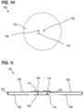
- FIG.1A to FIG.1C show a carrier 100 according to various embodiments.
- FIG.1A a front view
- FIG.1B a rear view
- FIG.1C a side view of the carrier 100.
- the carrier 100 can have a carrier plate 102.
- the carrier plate 102 can be, for example, a wafer (eg a wafer in any manufacturing state) or another substrate (eg a glass substrate).
- the carrier plate 102 can have a first side (hereinafter referred to as the front side, V) and a second side opposite the first side (hereinafter referred to as the back side, R).
- the carrier plate is shown in the figures as a round carrier (eg as wafer).
- the carrier plate 102 may also have any other shape (eg rectangular, eg square).
- the carrier plate 102 may have any desired size (eg adapted to the wafer chuck arranged in a process chamber).
- the carrier plate 102 may have any diameter, d, common for wafers (eg, the carrier plate 102 may be a 150-mm wafer, a 200-mm wafer, a 300-mm wafer, a 450-mm wafer, etc.).
- the carrier 100 can have a sensor arranged at least partially on the front side, V, of the carrier plate 102. In the following, the sensor is described by way of example as a quartz oscillator.
- the senor can also be any other type of sensor (e.g. a temperature sensor, a humidity sensor, etc.). It is also understood that the carrier 100 can have several such sensors. These several sensors can have the same type of sensor (e.g. each one a quartz oscillator) or can have different types of sensors from one another (e.g. the carrier 100 can have a quartz oscillator and a temperature sensor).
- the carrier 100 can have a quartz oscillator 104 arranged at least partially on the front side, V, of the carrier plate 102.
- the quartz oscillator 104 can have a first electrode and a second electrode.
- the carrier 100 can have a first electrode contact 106 and a second electrode contact 108 for contacting the quartz oscillator 104.
- the first electrode contact 106 can be electrically conductively connected to the first electrode of the quartz oscillator 104 and the second electrode contact 108 can be electrically conductively connected to the second electrode of the quartz oscillator 104.
- the first electrode contact 106 and the second electrode contact 108 can be arranged arbitrarily on the carrier plate 102. According to various embodiments, the first electrode contact 106 and the second electrode contact 108 can be arranged on the back side, R, of the carrier plate 102. It is understood that at least one of these electrode contacts 106, 108 can also be arranged on the front side, V, of the carrier plate 102. In this case, the wafer chuck 200 described herein can have corresponding contacts for contacting the at least one electrode contact on the front side, V, of the carrier plate 102.
- the quartz oscillator 104 can be configured as or used as a quartz crystal microbalance.
- the first electrode contact 106 arranged on the rear side, R, of the carrier plate 102 can be electrically connected to the first electrode of the quartz oscillator 104, for example by means of at least one first through-connection 110 (also referred to as via) formed in the carrier plate 102.
- the second electrode contact 108 arranged on the rear side, R, of the carrier plate 102 can be electrically connected to the second electrode of the quartz oscillator 104, for example by means of at least one second through-connection 120 formed in the carrier plate 102.
- the second electrode contact 108 can be connected to the second electrode of the quartz oscillator 104 by means of an electrically conductive layer formed on the surface of the carrier plate 102 (see, for example, FIG.1I ).
- the carrier 100 may have more than one quartz oscillator arranged on the front side, V, of the carrier plate 102.
- the plurality of quartz oscillators may be arranged at different positions of the carrier 100 so that during processing a respective layer thickness and/or layer thickness change can be detected at each of the different positions.
- FIG.1E to FIG.1I A corresponding example for two quartz oscillators is in FIG.1E to FIG.1I according to various embodiments.
- another quartz oscillator 114 can be arranged at least partially on the front side, V, of the carrier plate 102.
- the other quartz oscillator 114 can be configured similarly to the quartz oscillator 104.
- the other quartz oscillator can also have two electrodes (eg another first electrode and another second electrode).
- the carrier 100 can have another first electrode contact 116 (e.g. arranged on the back side, R, of the carrier plate 102) and another second electrode contact 118 (e.g. arranged on the back side, R, of the carrier plate 102).
- the other first electrode contact 116 can be electrically connected to the other first electrode of the other quartz oscillator 114 by means of at least one other first via 120.
- the other second electrode contact 118 can be electrically connected to the other second electrode of the other quartz oscillator 114 by means of at least one other second via.
- the carrier 100 may have the other first electrode contact 116 (eg arranged on the back side, R, of the carrier plate 102), but not the other second electrode contact 118 (eg arranged on the back side, R, of the carrier plate 102).
- the second electrode contact 108 may be a common electrode contact of the quartz oscillator 104 and the other quartz oscillator 114.
- the carrier 100 can, for example, have an electrically conductive layer which electrically connects the second electrode of the quartz oscillator 104 and the other second electrode of the other quartz oscillator 114 to the (common) second electrode contact 108.
- the carrier 100 described here can serve as a measuring wafer.
- various processes can be analyzed using this measuring wafer.
- the carrier 100 can be a wafer to be manufactured.
- the one or more quartz oscillators can be arranged on a wafer to be manufactured (e.g. in a manufacturing step) in order to analyze processes directly during manufacturing.
- the manufacturing of the wafer can be adapted in such a way that corresponding rear side contacts (as electrode contacts 106, 108, 116, 118) and optionally corresponding vias are provided beforehand.
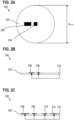
- FIG.2A and FIG.2B show a wafer chuck 200 according to various embodiments.
- the wafer chuck 200 may include a base plate 202.
- a conventional wafer chuck may be modified to the wafer chuck 200.
- the base plate 202 may be the conventional wafer chuck, for example.
- the base plate 202 may be configured to support (or hold) a carrier (eg, the carrier 100).
- the wafer chuck 200 may have any shape and size.
- the carrier may be a wafer, so that the base plate 202 may be configured to support the wafer.
- the base plate 202 may have a size (eg, a diameter, d chuck ) that is equal to or larger than a diameter, d, of the wafer (eg, the carrier 100).
- the wafer chuck 200 may have a plurality of electrical contacts, such as a first electrical contact 206 and a second electrical contact 208.
- the plurality of electrical contacts (e.g. the first electrical contact 206 and the second electrical contact 208) may be arranged on the same side of the wafer chuck 200. These plurality of electrical contacts may serve to electrically contact rear side contacts of the wafer. Alternatively, at least one of the plurality of electrical contacts may be arranged differently and may be configured such that it can electrically conductively contact a front side contact arranged on the front side of the wafer.
- first electrical contact 206 and the second electrical contact 208 are shown as contact surfaces. Alternatively, at least one of these contacts can be a contact pin.
- the plurality of electrical contacts may be configured to provide a signal path to a sensor arranged on the wafer (eg, quartz crystal 104) when the wafer is supported/held by the base plate (see, eg, description regarding FIG.3 ) .
- the wafer chuck 200 can have an interface 210.
- the interface 210 can be electrically conductively connected to the plurality of electrical contacts (eg the first electrical contact 206 and the second electrical contact 208).
- the interface 210 can be configured such that an electrical signal can be applied to and/or tapped off from the plurality of electrical contacts by means of the interface 210.
- At least one electrical contact of the plurality of electrical contacts may be arranged such that it is spaced apart from the wafer when the wafer is supported by the base plate 202.
- FIG.2C shows the wafer chuck 200 according to various embodiments.
- the plurality of electrical contacts may include, in addition to the first electrical contact 206 and the second electrical contact 208, another first electrical contact 216 and another second electrical contact 218. These may be coupled accordingly to the interface 210 for applying a corresponding other electrical sensor signal.
- the other quartz oscillator 114 of the carrier 100 can be electrically contacted by means of the other first electrical contact 216 and the other second electrical contact 218 when the carrier 100 is arranged on the wafer chuck 200.
- a common potential e.g. a ground potential
- the carrier 100 and the wafer chuck 200 may be aligned so that the carrier 100 may be disposed on the wafer chuck 200 and contacted accordingly.
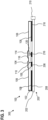
- FIG.3 shows a system 300 in which the carrier 100 is arranged on the wafer chuck 200, according to various embodiments.
- FIG.3 shows an exemplary design for two quartz oscillators. It is understood that the following explanations apply accordingly to fewer (i.e. one quartz oscillator) and for more than two quartz oscillators.
- Coupling between electrical contacts as described herein may be accomplished by direct physical contact of the electrical contacts. Alternatively, a gap may remain between the electrical contacts according to various embodiments.
- the carrier 100 and/or the wafer chuck 200 are configured such that the gap is present between two coupled contacts. This can, for example, significantly reduce wear and/or block a direct current contact.
- a respective sensor signal can be applied to the quartz oscillator 104 and the other quartz oscillator 114 via the coupled contacts.
- the change in layer thickness can be determined in a conventional manner by means of the quartz oscillator 104 and/or the other quartz oscillator 114.
- the deposition of a layer on the respective quartz oscillator and the Removing a layer deposited on the quartz oscillator leads to a change in the frequency of the quartz oscillator.
- This frequency change can be detected and from this the layer thickness change (and thus a layer thickness) can be determined.
- This frequency change can be detected (e.g. continuously) during layer deposition or removal (e.g. etching) and/or can be detected after the respective process.
- a frequency-dependent impedance of the respective quartz oscillator can be detected (e.g. measured).
- the frequency-dependent impedance of the quartz oscillator is dependent on the process-related frequency change, so that the layer thickness change can be determined based on the frequency-dependent impedance curve.
- applying the sensor signal to the quartz oscillator 104 can generate an oscillating circuit. If reference is made here to the resonant frequency of the quartz oscillator, it is understood that this resonant frequency only develops in the oscillating circuit (i.e. after the sensor signal is applied).
- a resonance frequency of the oscillating circuit generated by applying the sensor signal can be measured during the deposition of the layer (eg continuously). The resonance frequency can be detected, for example, with a minimum impedance (in a series oscillating circuit) or a maximum impedance (in a parallel oscillating circuit).
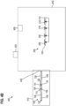
- FIG.4A shows a processing device 400 according to various embodiments.
- the processing device 400 can have a process chamber 402.
- the process chamber 402 can be coupled (eg by means of a corresponding opening (eg a flange)) to a pump system 404 for generating a negative pressure (eg vacuum) in the process chamber 402.
- the pump system 404 can have one or more vacuum pumps.
- a vacuum pump can be any type of vacuum pump, such as a high vacuum pump (eg a Turbomolecular pump) or a backing pump (e.g. a scroll pump, a diaphragm pump or a (e.g. multi-stage) Roots pump, a diffusion pump, rotary vane pump).
- the pump system 404 can be a combination of one or more of the above pumps.
- the pump system 404 can have a pumping station combined from a backing pump and a turbomolecular pump. It is understood that the process chamber 402 can be designed to achieve/maintain the negative pressure when closed, for example airtight, dusttight and/or vacuumtight.
- the negative pressure in the process chamber 402 can be a pressure (which is e.g. the external pressure) in a range from approximately 10 mbar to approximately 1 mbar (in other words, rough vacuum) or less, for example a pressure in a range from approximately 1 mbar to approximately 10 -3 mbar (in other words, fine vacuum) or less, for example a pressure in a range from approximately 10 -3 mbar to approximately 10 -7 mbar (in other words, high vacuum) or less, for example a pressure in a range of less than 10 -7 mbar (in other words, ultra-high vacuum).
- a pressure which is e.g. the external pressure in a range from approximately 10 mbar to approximately 1 mbar (in other words, rough vacuum) or less, for example a pressure in a range from approximately 1 mbar to approximately 10 -3 mbar (in other words, fine vacuum) or less, for example a pressure in a range from approximately 10 -3 mbar to approximately 10 -7 mbar (in
- the process chamber 402 can have at least one lock interface 406 for introducing and/or discharging the carrier 100.
- the carrier 100 can be arranged in an element 410 adjacent to it via the lock interface 406 before being introduced or after being discharging.
- the structure of the process chamber 402 can remain unchanged when introducing and/or discharging the carrier 100.
- the element 410 can be a pre-chamber.
- This pre-chamber can also be coupled to a corresponding pump system for generating a negative pressure.
- the pre-chamber can be closed by means of a slide (can also be referred to as a slide valve or gate) at the lock interface 406 may be vacuum separated from the process chamber 402.
- the carrier may be arranged in the pre-chamber, a negative pressure may be generated in the pre-chamber (generating a negative pressure in a chamber may also be referred to as evacuating the chamber), the slide may be opened and the carrier may be transferred into the process chamber 402 (eg onto the wafer chuck 200 arranged in the process chamber 402). It is understood that when transferring the carrier 100, one or more sample holders and/or one or more manipulators may be used.
- the element 410 can be a front opening unified pod (FOUP).
- FOUP front opening unified pod
- This can initially be vacuum decoupled by means of a slide, as described for the prechamber, and after arranging the FOUP at the lock interface 406, the slide can be opened and the carrier 100 can be fed from the FOUP into the process chamber 402 or ejected from the process chamber 402 into the FOUP.
- a FOUP can be arranged at the lock interface 406 of the process chamber 402
- the FOUP can also be arranged correspondingly at a lock interface of a prechamber connected to the process chamber 402 (e.g. vacuum-coupled) or another chamber connected to the process chamber 402 (e.g. vacuum-coupled).
- the element 410 may be an adjacent process chamber.
- the carrier 100 may be guided (eg transported) through the process chamber and the adjacent process chamber (in any order) one after the other.
- the processing device 400 may have a transport device (eg with a transport belt and/or transport rollers) for transporting the wafer arranged on the wafer chuck 200.
- carrier 100 through the process chamber and the adjacent process chamber.
- the wafer chuck 200 can also be moved in order to move the wafers, for example with reference to FIG.3 described measurements in each of the process chambers.
- the process chamber 402 may alternatively be opened and the carrier may subsequently be arranged (e.g., placed) on the wafer chuck 200. In this case, the process chamber 402 may be evacuated after arranging the carrier 100 on the wafer chuck 200.
- the processing device 400 can have a coating device 408 (eg arranged in the process chamber 402 and/or coupled to the process chamber 402).
- the coating device 408 can be set up such that a layer can be deposited on the front side of the carrier 100 (eg wafer) arranged on the wafer chuck 200. Consequently, the coating device 408 can be set up such that a coating process can be carried out in the process chamber 402 by means of the coating device 408.
- the coating process can be, for example, a physical vapor deposition process (PVD process) or a chemical vapor deposition process (CVD process).
- the PVD process can be, for example, electron beam evaporation, cathode sputtering, or the like.
- the CVD process can be, for example, atomic layer deposition (ALD for short). It is understood that atomic layer deposition can be considered a CVD process. When referred to herein as a CVD process, this can be, for example, ALD. As described herein, the carrier 100 (and the wafer chuck 200) is particularly advantageous for CVD processes, since these typically do not require in situ measurements of the Layer thickness and/or layer thickness change can be carried out.
- ALD atomic layer deposition
- the frequency of the quartz oscillator 104 and/or the other quartz oscillator 114 can be detected ex situ after the layer deposition (and/or after etching).
- materials, reactants or process gases may be introduced into the process chamber 402 during the coating process and/or that a temperature of the carrier 100 is changed (e.g., increased).
- a CVD process may be carried out at elevated temperatures (e.g., 100°C, 200°C, 300°C, etc.).
- the process gas may comprise an inert gas, such as argon, and/or a reactive gas, such as oxygen.
- a layer thickness of a layer deposited by means of the coating process and/or a layer deposition rate during the coating process can be determined.
- the carrier 100 arranged on the wafer chuck 200 can be transported from the process chamber 402 into the adjacent process chamber.
- the adjacent process chamber can also have a coating device for carrying out a coating process and the layer thickness and/or layer deposition rate associated with the coating process can be determined.
- the other process chamber can have a removal device for at least partially removing (eg etching) the layer deposited in the process chamber.
- a coating device that is used during the coating process can be used. and/or the layer thickness remaining after removal can be determined.
- a layer thickness change rate (e.g. an etching rate) can also be determined during removal.
- the carrier 100 can be additionally coated in yet another process chamber after being discharged from the process chamber 402 and/or a previously deposited layer can be at least partially removed (e.g. by means of an etching process). As described above, a layer thickness and/or a change in layer thickness can again be determined here. This clearly shows the reusability of the carrier 100 described here.
- the processing device 400 can have a control device.
- the control device can be set up to control the infeed and outfeed, the application of the sensor signal for generating the oscillating circuit, and/or the detection of the resonance frequency.
- the control device can be set up to provide the detected resonance frequency to an evaluation unit directly or indirectly (e.g. by means of one or more storage media).
- the quartz oscillator 104 is an example of a sensor and the carrier 100 may additionally or alternatively have any type of sensor.
- corresponding parameters can be detected by means of the sensor directly on the carrier 100 in the process chamber 402.
- the sensor can be a temperature sensor for detecting a temperature of the carrier 100.
- a change in the temperature of the carrier 100 can have various causes.
- the coating process can be a PVD process in which heat radiation is emitted.
- the processing device 400 can have a temperature control device which can be set up can increase (i.e. heating) or decrease (i.e. cooling) a temperature of the carrier 100.
- the coating process can be a CVD process in which the temperature of the carrier 100 is increased by means of the temperature control device.
- FIG.5 shows a flowchart of a method 500 according to various embodiments.
- the method 500 may include introducing a carrier (e.g. a wafer) into a process chamber (in 502).
- the carrier may include a carrier plate, a quartz oscillator arranged on the front side of the carrier plate, and a first electrode contact and a second electrode contact for contacting the quartz oscillator.
- the carrier may be configured according to the carrier 100.
- introducing the carrier may include transferring the carrier from a front opening unified pod (FOUP) (e.g. coupled to the process chamber directly or via intermediate chambers) into the process chamber.
- introducing the carrier may include introducing it using a prechamber.
- FOUP front opening unified pod
- the introduction by means of a prechamber can, for example, comprise: arranging the carrier in a prechamber coupled to the process chamber, evacuating the prechamber, opening a gate between the prechamber and the process chamber, and transferring the carrier from the prechamber into the process chamber.
- the method 500 may include coupling (eg, bringing into contact) the first electrode contact and the second electrode contact to an interface arranged in the process chamber (in 504).
- the interface may, for example, be an interface of a the wafer chuck arranged in the process chamber (e.g. the interface 210 of the wafer chuck 200).
- the method 500 may include applying a sensor signal to the quartz oscillator via the interface (in 506).
- a measurement signal may be detected while the sensor signal is being applied.
- the measurement signal may be, for example, an impedance of the quartz oscillator.
- the method 500 can further comprise depositing a layer (e.g. by means of chemical vapor deposition (CVD) and/or by means of physical vapor deposition (PVD)) on the carrier arranged in the process chamber.
- a layer e.g. by means of chemical vapor deposition (CVD) and/or by means of physical vapor deposition (PVD)
- the sensor signal can be applied to the quartz oscillator during the deposition of the layer. This makes it possible, for example, to monitor the change in the layer thickness during the deposition. A change in the layer thickness can also be detected in this way.
- the sensor signal can be applied to the quartz oscillator after the layer has been deposited. This makes it possible, for example, to determine the layer thickness of the deposited layer.
- the measurement accuracy can be significantly increased.
- the method 500 can further comprise discharging the carrier from the process chamber and introducing it into another process chamber.
- the first electrode contact and the second electrode contact of the carrier can be coupled to another interface, by means of which a sensor signal can be applied.
- another layer can now be deposited and the layer thickness or layer deposition rate can be recorded and/or the layer can be (at least) partially removed. (e.g. by etching) and the layer thickness remaining after removal or the removal rate (e.g. etching rate) can be recorded.
- a continuous process chain during processing of a wafer can be monitored and/or analyzed using the same sensor or sensors.
- Example 1 is a method comprising: introducing a carrier (e.g. a wafer) into a process chamber, the carrier comprising: a carrier plate, a sensor (e.g. quartz oscillator) arranged on the front side of the carrier plate, and a first electrode contact and a second electrode contact for contacting the sensor (e.g. the quartz oscillator); coupling (e.g. bringing into contact) the first electrode contact and the second electrode contact to an interface arranged in the process chamber; and applying a sensor signal to the sensor (e.g. to the quartz oscillator) by means of the interface.
- a carrier e.g. a wafer
- the carrier comprising: a carrier plate, a sensor (e.g. quartz oscillator) arranged on the front side of the carrier plate, and a first electrode contact and a second electrode contact for contacting the sensor (e.g. the quartz oscillator); coupling (e.g. bringing into contact) the first electrode contact and the second electrode contact to an interface arranged
- Example 2 is configured according to Example 1, wherein the structure of the process chamber is not changed when the carrier is introduced into the process chamber.
- Example 3 is a method according to example 1 or 2, wherein the introduction of the carrier into the process chamber comprises: arranging the carrier in a pre-chamber coupled to the process chamber; evacuating the pre-chamber; opening a slider between the pre-chamber and the process chamber; and transferring the carrier from the pre-chamber to the process chamber.
- Example 4 is configured according to example 1 or 2, wherein introducing the carrier into the process chamber comprises: transferring the carrier from a front opening unified pod (FOUP) (e.g. coupled to the process chamber) into the process chamber.
- FOUP front opening unified pod
- Example 5 is a method according to any one of Examples 1 to 4, wherein the interface is arranged at, on, or in a wafer chuck within the process chamber or is part of the wafer chuck; and wherein the first electrode contact and the second electrode contact are coupled to the interface by arranging (e.g., placing) the carrier on the wafer chuck.
- Example 6 the method according to any one of Examples 1 to 5 may optionally further comprise: depositing a layer (e.g. by means of chemical vapor deposition (CVD/ALD) and/or by means of physical vapor deposition (PVD)) on the carrier arranged in the process chamber.
- CVD/ALD chemical vapor deposition
- PVD physical vapor deposition
- the method according to example 6 can optionally further comprise that the sensor is a quartz oscillator and the method can further comprise: while applying the sensor signal to the quartz oscillator, measuring a resonance frequency of an oscillating circuit generated by applying the sensor signal. Additionally or alternatively, a frequency-dependent impedance can be measured.
- Example 8 the method according to Example 7 may optionally further comprise: determining a layer thickness of the deposited layer using the measured Resonance frequency of the quartz crystal.
- Example 9 is configured according to example 7 or 8, wherein the resonant frequency of the quartz oscillator is measured during the deposition of the layer, and wherein the method further comprises: determining a layer deposition rate during the deposition of the layer using the measured resonant frequency of the quartz oscillator.
- Example 10 is configured according to any one of Examples 6 to 9, wherein the layer is deposited by chemical vapor deposition (CVD), such as atomic layer deposition (ALD).
- CVD chemical vapor deposition
- ALD atomic layer deposition
- Example 11 is a method according to any one of Examples 6 to 10, further comprising: after depositing the layer, ejecting the carrier (e.g. the wafer) from the process chamber.
- the carrier e.g. the wafer
- Example 12 is configured according to Example 11, wherein discharging the carrier from the process chamber comprises: transferring the carrier from the process chamber into (e.g., the) Front Opening Unified Pod (FOUP).
- FOUP Front Opening Unified Pod
- Example 13 is a method according to example 11 or 12, further comprising: introducing the carrier (e.g. the wafer) into another process chamber; coupling (e.g. bringing into contact) the first electrode contact and the second electrode contact with another interface arranged in the other process chamber; and applying another sensor signal to the sensor (e.g. to the quartz oscillator) by means of the other interface.
- the carrier e.g. the wafer
- coupling e.g. bringing into contact
- the first electrode contact and the second electrode contact with another interface arranged in the other process chamber
- another sensor signal e.g. to the quartz oscillator
- Example 14 the method according to Example 13 may optionally further comprise: at least partially removing (eg etching) the layer, wherein the other sensor signal during removing (e.g. etching) the layer is applied to the quartz oscillator; and while applying the sensor signal to the sensor configured as the quartz oscillator, measuring a resonance frequency of the quartz oscillator.
- Example 15 is configured according to example 14, wherein the layer is only partially removed and wherein the method further comprises: determining a layer thickness of the layer after the partial removal of the layer using the measured resonance frequency of the quartz crystal.
- Example 16 is configured according to example 14 or 15, wherein the resonant frequency of the quartz oscillator is measured during removal (e.g., etching) of the layer, and wherein the method further comprises: determining a removal rate (e.g., etching rate) during removal of the layer using the measured resonant frequency of the quartz oscillator.
- a removal rate e.g., etching rate
- Example 17 is a carrier comprising: a carrier plate (e.g. a wafer) with a first side and a second side opposite the first side; a quartz oscillator with a first electrode and a second electrode, wherein the quartz oscillator is at least partially arranged on the first side of the carrier plate; and a first electrode contact and a second electrode contact on the second side of the carrier plate, wherein the first electrode contact is electrically conductively connected to the first electrode of the quartz oscillator and wherein the second electrode contact is electrically conductively connected to the second electrode of the quartz oscillator.
- a carrier plate e.g. a wafer
- a quartz oscillator with a first electrode and a second electrode, wherein the quartz oscillator is at least partially arranged on the first side of the carrier plate
- a first electrode contact and a second electrode contact on the second side of the carrier plate, wherein the first electrode contact is electrically conductively connected to the first electrode of the quartz oscillator and wherein the second electrode contact is
- Example 18 is configured according to Example 17, wherein the quartz oscillator in conjunction with the first electrode contact and the second electrode contact is configured as a quartz crystal microbalance.
- the carrier according to Example 17 or 18 can optionally further comprise: at least one first via, which is formed in the carrier plate and electrically connects the first electrode of the quartz oscillator to the first electrode contact.
- the carrier according to any one of examples 17 to 19 can optionally further comprise: at least one second via, which is formed in the carrier plate and electrically connects the second electrode of the quartz oscillator to the second electrode contact.
- Example 21 is configured according to any one of examples 17 to 18, wherein the carrier plate electrically connects the second electrode of the quartz oscillator to the second electrode contact.
- the carrier according to any one of examples 17 to 21 can optionally further comprise: another quartz oscillator with another first electrode and another second electrode, wherein the other quartz oscillator is at least partially arranged on the first side of the carrier plate; and another first electrode contact and another second electrode contact on the second side of the carrier plate, wherein the other first electrode contact is electrically conductively connected to the other first electrode of the other quartz oscillator and wherein the other second electrode contact is electrically conductively connected to the other second electrode of the other quartz oscillator.
- the carrier according to Example 22 can optionally further comprise: at least one other first via, which is formed in the carrier plate and electrically connects the other first electrode of the other quartz oscillator to the other first electrode contact; and at least one other second via, which is formed in the carrier plate and electrically connects the other second electrode of the other quartz oscillator with the other second electrode contact.
- the carrier according to any one of examples 17 to 21 can optionally further comprise: another quartz oscillator with another first electrode and another second electrode, wherein the other quartz oscillator is at least partially arranged on the first side of the carrier plate; and another electrode contact on the second side of the carrier plate, wherein the other electrode contact is electrically conductively connected to the other first electrode of the other quartz oscillator and wherein the other second electrode of the other quartz oscillator is electrically conductively connected to the second electrode contact.
- the carrier according to Example 24 can optionally further comprise: at least one other via which is formed in the carrier plate and electrically conductively connects the other first electrode of the other quartz oscillator to the other electrode contact; and wherein the carrier plate electrically conductively connects the other second electrode of the other quartz oscillator to the second electrode contact.
- Example 26 is a wafer chuck comprising: a base plate for supporting/holding a wafer; a plurality of electrical contacts (eg as a contact surface or as a contact pin) for providing a signal path to a sensor arranged on the wafer (eg to a quartz crystal) when the wafer is supported/held by the base plate; an interface electrically conductively connected to the plurality of electrical contacts, which is configured such that an electrical sensor signal can be applied to the plurality of electrical contacts by means of the interface.
- a plurality of electrical contacts eg as a contact surface or as a contact pin
- Example 27 is configured according to Example 26, wherein at least one electrical contact of the plurality of electrical contacts is arranged such that when a wafer is supported/held by the base plate, it is arranged at a distance from the wafer.
- Example 28 is configured according to example 26 or 27, wherein the sensor is a quartz crystal microbalance.
- Example 29 is a computer-readable medium (e.g., a computer program product, a non-transitory storage medium, a non-transitory storage medium, a non-volatile storage medium) capable of storing instructions that, when executed by a processor, cause the processor to control an apparatus to perform the method of one or more of the first example through the fifteenth example.
- a computer-readable medium e.g., a computer program product, a non-transitory storage medium, a non-transitory storage medium, a non-volatile storage medium
- the carrier in one or more of Examples 1 to 16 may be configured according to any of Examples 17 to 25 and that the carrier in one or more of Examples 1 to 16 may be disposed in the process chamber on a wafer chuck according to any of Examples 26 to 28.
Landscapes
- Chemical & Material Sciences (AREA)
- Chemical Kinetics & Catalysis (AREA)
- Engineering & Computer Science (AREA)
- Materials Engineering (AREA)
- Mechanical Engineering (AREA)
- Metallurgy (AREA)
- Organic Chemistry (AREA)
- General Chemical & Material Sciences (AREA)
- Crystallography & Structural Chemistry (AREA)
- Container, Conveyance, Adherence, Positioning, Of Wafer (AREA)
- Chemical Vapour Deposition (AREA)
Applications Claiming Priority (1)
| Application Number | Priority Date | Filing Date | Title |
|---|---|---|---|
| DE102022128091.8A DE102022128091B4 (de) | 2022-10-25 | 2022-10-25 | Wafer-Chuck, Träger und Verfahren |
Publications (2)
| Publication Number | Publication Date |
|---|---|
| EP4372121A2 true EP4372121A2 (fr) | 2024-05-22 |
| EP4372121A3 EP4372121A3 (fr) | 2024-07-17 |
Family
ID=88416872
Family Applications (1)
| Application Number | Title | Priority Date | Filing Date |
|---|---|---|---|
| EP23203999.0A Pending EP4372121A3 (fr) | 2022-10-25 | 2023-10-17 | Plateau de tranche, support et procédé |
Country Status (2)
| Country | Link |
|---|---|
| EP (1) | EP4372121A3 (fr) |
| DE (1) | DE102022128091B4 (fr) |
Family Cites Families (11)
| Publication number | Priority date | Publication date | Assignee | Title |
|---|---|---|---|---|
| JP2667682B2 (ja) * | 1988-09-26 | 1997-10-27 | 日本ケミコン株式会社 | 電子部品の実装構造および実装方法 |
| JPH0361368A (ja) * | 1989-07-28 | 1991-03-18 | Hitachi Nakaseiki Ltd | イオンスパッタリング方法およびその装置 |
| US6668618B2 (en) * | 2001-04-23 | 2003-12-30 | Agilent Technologies, Inc. | Systems and methods of monitoring thin film deposition |
| US6889568B2 (en) * | 2002-01-24 | 2005-05-10 | Sensarray Corporation | Process condition sensing wafer and data analysis system |
| US7828929B2 (en) * | 2004-12-30 | 2010-11-09 | Research Electro-Optics, Inc. | Methods and devices for monitoring and controlling thin film processing |
| US7977609B2 (en) * | 2005-12-22 | 2011-07-12 | Tokyo Electron Limited | Temperature measuring device using oscillating frequency signals |
| DE102006029039A1 (de) * | 2006-06-24 | 2007-12-27 | Carl Zeiss Smt Ag | Vorrichtung und Verfahren zur Überwachung von Materialbearbeitungsprozessen |
| DE102007061777B4 (de) * | 2007-12-19 | 2010-12-16 | Von Ardenne Anlagentechnik Gmbh | Verfahren zur Vakuumbeschichtung von zu beschichtenden Substraten und Vakkumbeschichtungsanlage |
| EP2309220A1 (fr) * | 2009-10-02 | 2011-04-13 | Applied Materials, Inc. | Dispositif et procédé pour mesurer l'épaisseur d'une couche |
| JP5696576B2 (ja) * | 2011-04-25 | 2015-04-08 | 東京エレクトロン株式会社 | 温度測定用基板及び熱処理装置 |
| US20170260629A1 (en) * | 2016-03-08 | 2017-09-14 | Ultratech, Inc. | Quartz crystal microbalance assembly for ALD systems |
-
2022
- 2022-10-25 DE DE102022128091.8A patent/DE102022128091B4/de active Active
-
2023
- 2023-10-17 EP EP23203999.0A patent/EP4372121A3/fr active Pending
Also Published As
| Publication number | Publication date |
|---|---|
| EP4372121A3 (fr) | 2024-07-17 |
| DE102022128091B4 (de) | 2024-06-06 |
| DE102022128091A1 (de) | 2024-04-25 |
Similar Documents
| Publication | Publication Date | Title |
|---|---|---|
| DE3853904T2 (de) | Verfahren zur bestimmung des endpunktes bei der reinigung in einem apparat zur herstellung von halbleiterbauelementen. | |
| DE69424759T2 (de) | Gasphasenabscheidungsverfahren in einer einzigen Kammer für Dünnfilmtransistoren | |
| DE10109507B4 (de) | Halbleiterherstellungsverfahren | |
| DE2703659C2 (de) | Ätzvorrichtung zum Ätzen eines Objekts unter Verwendung von Plasma | |
| DE69133254T2 (de) | Arbeitsverfahren für Vakuumbehandlungsvorrichtung | |
| DE69032189T2 (de) | Peripherieabdichtung für Halbleiterplättchen und verfahren zu deren Verwendung | |
| DE19832566C2 (de) | Niederdruck-CVD-Vorrichtung für die Herstellung von Halbleiterbauelementen, ihr Betriebsverfahren und Optimierungsverfahren eines Reinigungsverfahrens für eine Prozesskammer | |
| DE69011052T2 (de) | Chemische Gasphasen-Beschichtungsanlage der In-Line-Bauart. | |
| DE69808535T2 (de) | Verfahren zur Herstellung einer organischen elektrolumineszenten Vorrichtung | |
| DE3047441A1 (de) | Vorrichtung zum beschichten von mikroplaettchen | |
| DE69801291T2 (de) | Innenbeschichtung von Vakuumbehältern | |
| EP3020063A1 (fr) | Spectromètre de masse, son utilisation, ainsi que procédé d'analyse d'un mélange gazeux par spectrométrie de masse | |
| DE69610365T2 (de) | Haftschicht für die Abscheidung von Wolfram | |
| DE69715962T2 (de) | Plasma Behandlung Anlage und Behandlung-Methode | |
| DE19606463C2 (de) | Mehrkammer-Kathodenzerstäubungsvorrichtung | |
| DE68914963T2 (de) | Radiofrequenzquadrupolbeschleunigung mit Aussenresonanzkreis. | |
| DE112010000869T5 (de) | Plasmaverarbeitungsvorrichtung | |
| DE69108285T2 (de) | Peripherieabdichtung für Halbleiterplättchen durch Gasinjektion. | |
| DE102022128091B4 (de) | Wafer-Chuck, Träger und Verfahren | |
| DE69603569T2 (de) | Verfahren zur Substratschadensreduzierung bei PECVD | |
| DE102017202960A1 (de) | Quarzkristall-Mikrowaagen-Aufbau für ALD-Systeme | |
| DE102017108290B4 (de) | Plasmavorrichtung | |
| DE69111540T2 (de) | Vorrichtung zum Herstellen einer Schicht im Vacuum. | |
| US20220064783A1 (en) | Sputtering system and deposition method | |
| DE112010000717T5 (de) | Plasmaverarbeitungsvorrichtung |
Legal Events
| Date | Code | Title | Description |
|---|---|---|---|
| PUAI | Public reference made under article 153(3) epc to a published international application that has entered the european phase |
Free format text: ORIGINAL CODE: 0009012 |
|
| STAA | Information on the status of an ep patent application or granted ep patent |
Free format text: STATUS: THE APPLICATION HAS BEEN PUBLISHED |
|
| AK | Designated contracting states |
Kind code of ref document: A2 Designated state(s): AL AT BE BG CH CY CZ DE DK EE ES FI FR GB GR HR HU IE IS IT LI LT LU LV MC ME MK MT NL NO PL PT RO RS SE SI SK SM TR |
|
| PUAL | Search report despatched |
Free format text: ORIGINAL CODE: 0009013 |
|
| AK | Designated contracting states |
Kind code of ref document: A3 Designated state(s): AL AT BE BG CH CY CZ DE DK EE ES FI FR GB GR HR HU IE IS IT LI LT LU LV MC ME MK MT NL NO PL PT RO RS SE SI SK SM TR |
|
| RIC1 | Information provided on ipc code assigned before grant |
Ipc: G01K 7/02 20210101ALI20240611BHEP Ipc: H01L 21/67 20060101ALI20240611BHEP Ipc: C23C 16/52 20060101ALI20240611BHEP Ipc: C23C 16/458 20060101ALI20240611BHEP Ipc: C23C 14/54 20060101ALI20240611BHEP Ipc: C23C 14/52 20060101ALI20240611BHEP Ipc: C23C 14/50 20060101AFI20240611BHEP |
|
| STAA | Information on the status of an ep patent application or granted ep patent |
Free format text: STATUS: REQUEST FOR EXAMINATION WAS MADE |
|
| 17P | Request for examination filed |
Effective date: 20250117 |