EP4372807B1 - Substratanordnung und verfahren zur herstellung einer substratanordnung - Google Patents
Substratanordnung und verfahren zur herstellung einer substratanordnung Download PDFInfo
- Publication number
- EP4372807B1 EP4372807B1 EP22207915.4A EP22207915A EP4372807B1 EP 4372807 B1 EP4372807 B1 EP 4372807B1 EP 22207915 A EP22207915 A EP 22207915A EP 4372807 B1 EP4372807 B1 EP 4372807B1
- Authority
- EP
- European Patent Office
- Prior art keywords
- nanowires
- metallization layer
- layer
- subset
- substrate
- Prior art date
- Legal status (The legal status is an assumption and is not a legal conclusion. Google has not performed a legal analysis and makes no representation as to the accuracy of the status listed.)
- Active
Links
Images

Classifications
-
- H—ELECTRICITY
- H10—SEMICONDUCTOR DEVICES; ELECTRIC SOLID-STATE DEVICES NOT OTHERWISE PROVIDED FOR
- H10W—GENERIC PACKAGES, INTERCONNECTIONS, CONNECTORS OR OTHER CONSTRUCTIONAL DETAILS OF DEVICES COVERED BY CLASS H10
- H10W99/00—Subject matter not provided for in other groups of this subclass
-
- H—ELECTRICITY
- H10—SEMICONDUCTOR DEVICES; ELECTRIC SOLID-STATE DEVICES NOT OTHERWISE PROVIDED FOR
- H10W—GENERIC PACKAGES, INTERCONNECTIONS, CONNECTORS OR OTHER CONSTRUCTIONAL DETAILS OF DEVICES COVERED BY CLASS H10
- H10W70/00—Package substrates; Interposers; Redistribution layers [RDL]
- H10W70/60—Insulating or insulated package substrates; Interposers; Redistribution layers
- H10W70/611—Insulating or insulated package substrates; Interposers; Redistribution layers for connecting multiple chips together
-
- B—PERFORMING OPERATIONS; TRANSPORTING
- B82—NANOTECHNOLOGY
- B82Y—SPECIFIC USES OR APPLICATIONS OF NANOSTRUCTURES; MEASUREMENT OR ANALYSIS OF NANOSTRUCTURES; MANUFACTURE OR TREATMENT OF NANOSTRUCTURES
- B82Y10/00—Nanotechnology for information processing, storage or transmission, e.g. quantum computing or single electron logic
-
- H—ELECTRICITY
- H10—SEMICONDUCTOR DEVICES; ELECTRIC SOLID-STATE DEVICES NOT OTHERWISE PROVIDED FOR
- H10W—GENERIC PACKAGES, INTERCONNECTIONS, CONNECTORS OR OTHER CONSTRUCTIONAL DETAILS OF DEVICES COVERED BY CLASS H10
- H10W70/00—Package substrates; Interposers; Redistribution layers [RDL]
- H10W70/01—Manufacture or treatment
- H10W70/05—Manufacture or treatment of insulating or insulated package substrates, or of interposers, or of redistribution layers
-
- H—ELECTRICITY
- H10—SEMICONDUCTOR DEVICES; ELECTRIC SOLID-STATE DEVICES NOT OTHERWISE PROVIDED FOR
- H10W—GENERIC PACKAGES, INTERCONNECTIONS, CONNECTORS OR OTHER CONSTRUCTIONAL DETAILS OF DEVICES COVERED BY CLASS H10
- H10W70/00—Package substrates; Interposers; Redistribution layers [RDL]
- H10W70/60—Insulating or insulated package substrates; Interposers; Redistribution layers
- H10W70/62—Insulating or insulated package substrates; Interposers; Redistribution layers characterised by their interconnections
- H10W70/65—Shapes or dispositions of interconnections
- H10W70/658—Shapes or dispositions of interconnections for devices provided for in groups H10D8/00 - H10D48/00
-
- H—ELECTRICITY
- H10—SEMICONDUCTOR DEVICES; ELECTRIC SOLID-STATE DEVICES NOT OTHERWISE PROVIDED FOR
- H10W—GENERIC PACKAGES, INTERCONNECTIONS, CONNECTORS OR OTHER CONSTRUCTIONAL DETAILS OF DEVICES COVERED BY CLASS H10
- H10W70/00—Package substrates; Interposers; Redistribution layers [RDL]
- H10W70/60—Insulating or insulated package substrates; Interposers; Redistribution layers
- H10W70/67—Insulating or insulated package substrates; Interposers; Redistribution layers characterised by their insulating layers or insulating parts
- H10W70/68—Shapes or dispositions thereof
- H10W70/685—Shapes or dispositions thereof comprising multiple insulating layers
-
- H—ELECTRICITY
- H10—SEMICONDUCTOR DEVICES; ELECTRIC SOLID-STATE DEVICES NOT OTHERWISE PROVIDED FOR
- H10W—GENERIC PACKAGES, INTERCONNECTIONS, CONNECTORS OR OTHER CONSTRUCTIONAL DETAILS OF DEVICES COVERED BY CLASS H10
- H10W74/00—Encapsulations, e.g. protective coatings
- H10W74/10—Encapsulations, e.g. protective coatings characterised by their shape or disposition
- H10W74/111—Encapsulations, e.g. protective coatings characterised by their shape or disposition the semiconductor body being completely enclosed
- H10W74/114—Encapsulations, e.g. protective coatings characterised by their shape or disposition the semiconductor body being completely enclosed by a substrate and the encapsulations
-
- H—ELECTRICITY
- H10—SEMICONDUCTOR DEVICES; ELECTRIC SOLID-STATE DEVICES NOT OTHERWISE PROVIDED FOR
- H10W—GENERIC PACKAGES, INTERCONNECTIONS, CONNECTORS OR OTHER CONSTRUCTIONAL DETAILS OF DEVICES COVERED BY CLASS H10
- H10W74/00—Encapsulations, e.g. protective coatings
- H10W74/10—Encapsulations, e.g. protective coatings characterised by their shape or disposition
- H10W74/111—Encapsulations, e.g. protective coatings characterised by their shape or disposition the semiconductor body being completely enclosed
- H10W74/121—Encapsulations, e.g. protective coatings characterised by their shape or disposition the semiconductor body being completely enclosed by multiple encapsulations, e.g. by a thin protective coating and a thick encapsulation
-
- H—ELECTRICITY
- H10—SEMICONDUCTOR DEVICES; ELECTRIC SOLID-STATE DEVICES NOT OTHERWISE PROVIDED FOR
- H10W—GENERIC PACKAGES, INTERCONNECTIONS, CONNECTORS OR OTHER CONSTRUCTIONAL DETAILS OF DEVICES COVERED BY CLASS H10
- H10W76/00—Containers; Fillings or auxiliary members therefor; Seals
- H10W76/10—Containers or parts thereof
- H10W76/12—Containers or parts thereof characterised by their shape
- H10W76/15—Containers comprising an insulating or insulated base
-
- H—ELECTRICITY
- H10—SEMICONDUCTOR DEVICES; ELECTRIC SOLID-STATE DEVICES NOT OTHERWISE PROVIDED FOR
- H10W—GENERIC PACKAGES, INTERCONNECTIONS, CONNECTORS OR OTHER CONSTRUCTIONAL DETAILS OF DEVICES COVERED BY CLASS H10
- H10W76/00—Containers; Fillings or auxiliary members therefor; Seals
- H10W76/40—Fillings or auxiliary members in containers, e.g. centering rings
- H10W76/42—Fillings
- H10W76/47—Solid or gel fillings
-
- H—ELECTRICITY
- H10—SEMICONDUCTOR DEVICES; ELECTRIC SOLID-STATE DEVICES NOT OTHERWISE PROVIDED FOR
- H10W—GENERIC PACKAGES, INTERCONNECTIONS, CONNECTORS OR OTHER CONSTRUCTIONAL DETAILS OF DEVICES COVERED BY CLASS H10
- H10W90/00—Package configurations
-
- H—ELECTRICITY
- H10—SEMICONDUCTOR DEVICES; ELECTRIC SOLID-STATE DEVICES NOT OTHERWISE PROVIDED FOR
- H10W—GENERIC PACKAGES, INTERCONNECTIONS, CONNECTORS OR OTHER CONSTRUCTIONAL DETAILS OF DEVICES COVERED BY CLASS H10
- H10W40/00—Arrangements for thermal protection or thermal control
- H10W40/20—Arrangements for cooling
- H10W40/25—Arrangements for cooling characterised by their materials
- H10W40/255—Arrangements for cooling characterised by their materials having a laminate or multilayered structure, e.g. direct bond copper [DBC] ceramic substrates
-
- H—ELECTRICITY
- H10—SEMICONDUCTOR DEVICES; ELECTRIC SOLID-STATE DEVICES NOT OTHERWISE PROVIDED FOR
- H10W—GENERIC PACKAGES, INTERCONNECTIONS, CONNECTORS OR OTHER CONSTRUCTIONAL DETAILS OF DEVICES COVERED BY CLASS H10
- H10W40/00—Arrangements for thermal protection or thermal control
- H10W40/20—Arrangements for cooling
- H10W40/25—Arrangements for cooling characterised by their materials
- H10W40/258—Metallic materials
-
- H—ELECTRICITY
- H10—SEMICONDUCTOR DEVICES; ELECTRIC SOLID-STATE DEVICES NOT OTHERWISE PROVIDED FOR
- H10W—GENERIC PACKAGES, INTERCONNECTIONS, CONNECTORS OR OTHER CONSTRUCTIONAL DETAILS OF DEVICES COVERED BY CLASS H10
- H10W72/00—Interconnections or connectors in packages
- H10W72/01—Manufacture or treatment
- H10W72/013—Manufacture or treatment of die-attach connectors
- H10W72/01331—Manufacture or treatment of die-attach connectors using blanket deposition
- H10W72/01338—Manufacture or treatment of die-attach connectors using blanket deposition in gaseous form, e.g. by CVD or PVD
-
- H—ELECTRICITY
- H10—SEMICONDUCTOR DEVICES; ELECTRIC SOLID-STATE DEVICES NOT OTHERWISE PROVIDED FOR
- H10W—GENERIC PACKAGES, INTERCONNECTIONS, CONNECTORS OR OTHER CONSTRUCTIONAL DETAILS OF DEVICES COVERED BY CLASS H10
- H10W72/00—Interconnections or connectors in packages
- H10W72/071—Connecting or disconnecting
- H10W72/073—Connecting or disconnecting of die-attach connectors
- H10W72/07331—Connecting techniques
- H10W72/07332—Compression bonding, e.g. thermocompression bonding
-
- H—ELECTRICITY
- H10—SEMICONDUCTOR DEVICES; ELECTRIC SOLID-STATE DEVICES NOT OTHERWISE PROVIDED FOR
- H10W—GENERIC PACKAGES, INTERCONNECTIONS, CONNECTORS OR OTHER CONSTRUCTIONAL DETAILS OF DEVICES COVERED BY CLASS H10
- H10W72/00—Interconnections or connectors in packages
- H10W72/071—Connecting or disconnecting
- H10W72/073—Connecting or disconnecting of die-attach connectors
- H10W72/07351—Connecting or disconnecting of die-attach connectors characterised by changes in properties of the die-attach connectors during connecting
- H10W72/07352—Connecting or disconnecting of die-attach connectors characterised by changes in properties of the die-attach connectors during connecting changes in structures or sizes
-
- H—ELECTRICITY
- H10—SEMICONDUCTOR DEVICES; ELECTRIC SOLID-STATE DEVICES NOT OTHERWISE PROVIDED FOR
- H10W—GENERIC PACKAGES, INTERCONNECTIONS, CONNECTORS OR OTHER CONSTRUCTIONAL DETAILS OF DEVICES COVERED BY CLASS H10
- H10W72/00—Interconnections or connectors in packages
- H10W72/30—Die-attach connectors
- H10W72/321—Structures or relative sizes of die-attach connectors
-
- H—ELECTRICITY
- H10—SEMICONDUCTOR DEVICES; ELECTRIC SOLID-STATE DEVICES NOT OTHERWISE PROVIDED FOR
- H10W—GENERIC PACKAGES, INTERCONNECTIONS, CONNECTORS OR OTHER CONSTRUCTIONAL DETAILS OF DEVICES COVERED BY CLASS H10
- H10W72/00—Interconnections or connectors in packages
- H10W72/30—Die-attach connectors
- H10W72/351—Materials of die-attach connectors
- H10W72/352—Materials of die-attach connectors comprising metals or metalloids, e.g. solders
-
- H—ELECTRICITY
- H10—SEMICONDUCTOR DEVICES; ELECTRIC SOLID-STATE DEVICES NOT OTHERWISE PROVIDED FOR
- H10W—GENERIC PACKAGES, INTERCONNECTIONS, CONNECTORS OR OTHER CONSTRUCTIONAL DETAILS OF DEVICES COVERED BY CLASS H10
- H10W72/00—Interconnections or connectors in packages
- H10W72/851—Dispositions of multiple connectors or interconnections
- H10W72/874—On different surfaces
- H10W72/884—Die-attach connectors and bond wires
-
- H—ELECTRICITY
- H10—SEMICONDUCTOR DEVICES; ELECTRIC SOLID-STATE DEVICES NOT OTHERWISE PROVIDED FOR
- H10W—GENERIC PACKAGES, INTERCONNECTIONS, CONNECTORS OR OTHER CONSTRUCTIONAL DETAILS OF DEVICES COVERED BY CLASS H10
- H10W74/00—Encapsulations, e.g. protective coatings
-
- H—ELECTRICITY
- H10—SEMICONDUCTOR DEVICES; ELECTRIC SOLID-STATE DEVICES NOT OTHERWISE PROVIDED FOR
- H10W—GENERIC PACKAGES, INTERCONNECTIONS, CONNECTORS OR OTHER CONSTRUCTIONAL DETAILS OF DEVICES COVERED BY CLASS H10
- H10W90/00—Package configurations
- H10W90/701—Package configurations characterised by the relative positions of pads or connectors relative to package parts
- H10W90/731—Package configurations characterised by the relative positions of pads or connectors relative to package parts of die-attach connectors
- H10W90/734—Package configurations characterised by the relative positions of pads or connectors relative to package parts of die-attach connectors between a chip and a stacked insulating package substrate, interposer or RDL
-
- H—ELECTRICITY
- H10—SEMICONDUCTOR DEVICES; ELECTRIC SOLID-STATE DEVICES NOT OTHERWISE PROVIDED FOR
- H10W—GENERIC PACKAGES, INTERCONNECTIONS, CONNECTORS OR OTHER CONSTRUCTIONAL DETAILS OF DEVICES COVERED BY CLASS H10
- H10W90/00—Package configurations
- H10W90/701—Package configurations characterised by the relative positions of pads or connectors relative to package parts
- H10W90/731—Package configurations characterised by the relative positions of pads or connectors relative to package parts of die-attach connectors
- H10W90/736—Package configurations characterised by the relative positions of pads or connectors relative to package parts of die-attach connectors between a chip and a stacked lead frame, conducting package substrate or heat sink
-
- H—ELECTRICITY
- H10—SEMICONDUCTOR DEVICES; ELECTRIC SOLID-STATE DEVICES NOT OTHERWISE PROVIDED FOR
- H10W—GENERIC PACKAGES, INTERCONNECTIONS, CONNECTORS OR OTHER CONSTRUCTIONAL DETAILS OF DEVICES COVERED BY CLASS H10
- H10W90/00—Package configurations
- H10W90/701—Package configurations characterised by the relative positions of pads or connectors relative to package parts
- H10W90/751—Package configurations characterised by the relative positions of pads or connectors relative to package parts of bond wires
- H10W90/754—Package configurations characterised by the relative positions of pads or connectors relative to package parts of bond wires between a chip and a stacked insulating package substrate, interposer or RDL
-
- H—ELECTRICITY
- H10—SEMICONDUCTOR DEVICES; ELECTRIC SOLID-STATE DEVICES NOT OTHERWISE PROVIDED FOR
- H10W—GENERIC PACKAGES, INTERCONNECTIONS, CONNECTORS OR OTHER CONSTRUCTIONAL DETAILS OF DEVICES COVERED BY CLASS H10
- H10W90/00—Package configurations
- H10W90/701—Package configurations characterised by the relative positions of pads or connectors relative to package parts
- H10W90/751—Package configurations characterised by the relative positions of pads or connectors relative to package parts of bond wires
- H10W90/756—Package configurations characterised by the relative positions of pads or connectors relative to package parts of bond wires between a chip and a stacked lead frame, conducting package substrate or heat sink
Definitions
- the instant disclosure relates to a substrate arrangement, in particular to a substrate arrangement for a power semiconductor module arrangement, and to methods for producing such a substrate arrangement.
- Power semiconductor module arrangements often include at least one semiconductor substrate arranged in a housing.
- a semiconductor arrangement including a plurality of controllable semiconductor elements e.g., two IGBTs in a half-bridge configuration
- Each substrate usually comprises a substrate layer (e.g., a ceramic layer), a first metallization layer deposited on a first side of the substrate layer and a second metallization layer deposited on a second side of the substrate layer.
- the controllable semiconductor elements are mounted, for example, on the first metallization layer.
- the second metallization layer may optionally be attached to a base plate or heat sink.
- the substrate arrangement further includes an encapsulant, wherein the encapsulant consists of or includes a silicone gel and directly adjoins the second ends of a second subset of the plurality of nanowires and fills any gaps and spaces between the nanowires of the second subset.
- the encapsulant consists of or includes a silicone gel and directly adjoins the second ends of a second subset of the plurality of nanowires and fills any gaps and spaces between the nanowires of the second subset.
- An electrical line or electrical connection as described herein may be a single electrically conductive element, or include at least two individual electrically conductive elements connected in series and/or parallel. Electrical lines and electrical connections may include metal and/or semiconductor material, and may be permanently electrically conductive (i.e., non-switchable).
- a semiconductor body as described herein may be made from (doped) semiconductor material and may be a semiconductor chip or be included in a semiconductor chip. A semiconductor body has electrically connecting pads and includes at least one semiconductor element with electrodes.
- the power semiconductor module arrangement 100 includes a housing 7 and a substrate 10.
- the substrate 10 includes a dielectric insulation layer 11, a (structured) first metallization layer 111 attached to the dielectric insulation layer 11, and a (structured) second metallization layer 112 attached to the dielectric insulation layer 11.
- the dielectric insulation layer 11 is disposed between the first and second metallization layers 111, 112.
- Each of the first and second metallization layers 111, 112 may consist of or include one of the following materials: copper; a copper alloy; aluminum; an aluminum alloy; any other metal or alloy that remains solid during the operation of the power semiconductor module arrangement.
- the substrate 10 may be a ceramic substrate, that is, a substrate in which the dielectric insulation layer 11 is a ceramic, e.g., a thin ceramic layer.
- the ceramic may consist of or include one of the following materials: aluminum oxide; aluminum nitride; zirconium oxide; silicon nitride; boron nitride; or any other dielectric ceramic.
- the dielectric insulation layer 11 may consist of or include one of the following materials: Al 2 O 3 , AIN, SiC, BeO or Si 3 N 4 .
- the power semiconductor module arrangement 100 further includes an encapsulant 5.
- the encapsulant 5 consists of or includes a silicone gel for example.
- the encapsulant 5 may at least partly fill the interior of the housing 7, thereby covering the components and electrical connections that are arranged on the substrate 10.
- the terminal elements 4 may be partly embedded in the encapsulant 5. At least their second ends 42, however, are not covered by the encapsulant 5 and protrude from the encapsulant 5 through the housing 7 to the outside of the housing 7.
- the encapsulant 5 is configured to protect the components and electrical connections of the power semiconductor module 100, in particular the components arranged on the substrate 10 inside the housing 7, from certain environmental conditions and mechanical damage.
- an electrically conductive connection layer 30 may have several drawbacks. For example, a plurality of different steps may have to be performed when forming an electrically conductive connection layer 30 (e.g., solder layer, a layer of an electrically conductive adhesive, or a layer of a sintered metal powder).
- the first connection partner 610 may be a substrate for a power semiconductor module, for example.
- the second connection partner 620 may be a semiconductor body, a terminal element, or any other component that is to be mounted to the substrate, for example. It is, however, also possible that the first connection partner 610 is a heat sink or base plate, and the second connection partner 620 is a substrate.
- a plurality of nanowires 612 is formed on a surface of the first connection partner 610 which faces the second connection partner 620.
- a second plurality of nanowires 612 is formed on a surface of the second connection partner 620 which faces the first connection partner 610.
- Each of the plurality of nanowires 612 has a first end and a second end. A first end of each of the plurality of nanowires 612 is inseparably connected to the surface of the first connection partner 610. A first end of each of the second plurality of nanowires 612 is inseparably connected to the surface of the second connection partner.
- the first and second connection partners 610, 620 are arranged at a certain distance from each other. The second ends of the plurality of nanowires 612 and the second ends of the second plurality of nanowires 612 are free ends.
- the surface of the first connection partner 610 on which the plurality of nanowires 612 is formed and the surface of the second connection partner 620 on which the second plurality of nanowires 612 is formed may consist of the same material such as, e.g., Al, an Al alloy, Cu, a Cu alloy, Ag, an Ag alloy, Au, or an Au alloy.
- the first connection partner 610 and the second connection partner 620 are then moved towards each other such that the second ends of the plurality of nanowires 612 contact the surface of the second connection partner 620, and the second ends of the second plurality of nanowires 612 contact the surface of the first connection partner 610.
- the second ends of the plurality of nanowires 612 may be inseparably connected to the surface of the second connection partner 620, and the second ends of the second plurality of nanowires 612 may be inseparably connected to the surface of the first connection partner 610.
- a permanent connection between the first connection partner 610 and the second connection partner 620 may be formed by means of the nanowires 612.
- nanowires 612 designates any element having the form of a wire, i.e. a length that is several times larger than its diameter, wherein the dimensions of the element are in the nanometer range.
- nanotubes or nanorods may also be used and are considered to fall under the term nanowire as used herein.
- a nanowire 612 is a nanostructure in the form of a wire having a nanorange diameter.
- a diameter of a nanowire 612 may be between 500nm and 1200nm.
- the nanowires 612 may have a length between their first end and their second end of between 10 ⁇ m and 70 ⁇ m, for example.
- the nanowires 612 generally extend perpendicular to the surface on which they are formed. Therefore, all nanowires 612 may have the same length such that the second ends of all of the nanowires 612 extend all the way to the surface of the other connection partner.
- the nanowires 612 may comprise or consist of carbon, cobalt, copper, silicon, or gold, for example.
- the first and the second connection partners 610, 620 are each provided with nanowires 612. This, however, is only an example. As is schematically illustrated in Figure 3A , it is also possible to form nanowires 612 only on one of the two connection partners. In the example illustrated in Figure 2B , the plurality of nanowires 612 formed on the first connection partner 610 and the second plurality of nanowires 612 formed on the second connection partner 620 can be considered to intertwine when the first and second connection partner 610, 620 are arranged close enough to each other and a permanent connection is formed between the two connection partners 610, 620.
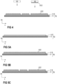
- the substrate arrangement may comprise a substrate 10, similar to what has been described with respect to Figure 1 above.
- the dielectric insulation layer 11, however, may also be omitted.
- the metallization layer 111 for example, may also be a so-called lead frame (die pad). That is, the substrate arrangement may solely comprise a metallization layer 111 and no dielectric insulation layer 11.
- the substrate 10 that is schematically illustrated in Figure 4 comprises a dielectric insulation layer 11 and a first metallization layer 111 attached to a first side of the dielectric insulation layer 11.
- the substrate 10, optionally, may further comprise a second metallization layer (not specifically illustrated in Figure 4 ).
- the section of the surface area of the first metallization layer 111 covered by the plurality of nanowires 612 is between 60% and 100%, or between 70% and 100% of the entire surface area of the first metallization layer 111.
- the first metallization layer 111 is a structured layer. All of the different sections of the first metallization layer 111 may be entirely covered by nanowires 612. It is, however, also possible that one or more, but not all sections of the first metallization layer 111 remain free of nanowires 612. Additionally or alternatively it is also possible that one or more sections are only partly covered by nanowires 612.
- the nanowires 612 are generally formed on the first metallization layer 111 before any components (e.g., semiconductor bodies 20, terminal elements 4, or any other components) are arranged on the substrate 10.
- any components e.g., semiconductor bodies 20, terminal elements 4, or any other components
- the substrate 10 may be equipped with components very flexibly.
- the section that is covered by the nanowires 612 is larger than the area required for mounting the components 20, 4 to the metallization layer 111. In this way, the components that are to be arranged on the substrate 10 do not have to be mounted to any specifically dedicated areas. That is, the substrate arrangement can be sold to different customers, irrespective of the specific design of the customer.
- a different subset of the plurality of nanowires 612 is arranged between each of the at least one component 20, 4 and the first metallization layer 111, wherein the second end of each nanowire 612 of the at least one subset is inseparably connected to a surface of the respective component 20, 4 such that each subset of nanowires 612 forms a permanent connection between the respective component 20, 4 and the first metallization layer 111.
- the number of nanowires 612 comprised in the at least one subset of nanowires 612 is less than the number of nanowires 612 comprised in the plurality of nanowires 612. That is, the second ends of at least one other subset of nanowires 612 are free ends that are not connected to any component 20, 4.
- a method for producing a substrate arrangement comprises forming a first metallization layer 111, forming a plurality of nanowires 612 on a surface of the first metallization layer 111, and arranging at least one component 20, 4 on the first metallization layer 111 such that a first subset of the plurality of nanowires is arranged between the first metallization layer and the at least one component, wherein the plurality of nanowires 612 is evenly distributed over a section of the surface area or over the entire surface area of the first metallization layer 111, each of the plurality of nanowires 612 comprises a first end and a second end, wherein the first end of each of the plurality nanowires 612 is inseparably connected to the surface of the first metallization layer 111, the second end of each nanowire of the first subset is inseparably connected to a surface of one of the at least one component 20, 4 such that the first subset of nanowires forms a permanent connection between the first metallization layer 111 and
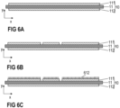
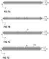
- nanowires 612 can only be formed on metallic surfaces. Therefore, if the first metallization layer 111 is structured first, as is exemplarily illustrated in Figure 6 , generally no nanowires 612 will form on those sections of the dielectric insulation layer 11, which are no longer covered by the first metallization layer 111. As has been described with respect to Figure 1 above, the dielectric insulation layer 11 generally does not comprise any metallic surfaces. Therefore, no nanowires 612 will grow on the surfaces of the dielectric insulation layer 11.
- a masking layer 70 after structuring the first metallization layer (see Figure 7B ) and before forming the plurality of nanowires 612, as is schematically illustrated in Figure 7C .
- the masking layer 70 may be formed on those sections of the dielectric insulation layer 11 that are not covered by the first metallization layer 111, thereby preventing nanowires 612 from being formed on the dielectric insulation layer 11. Once the nanowires 612 have been formed, the masking layer 70 may be removed (not specifically illustrated).
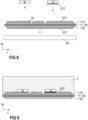
- components such as, e.g., semiconductor bodies 20, may be mounted on the surface of the first metallization layer 111.
- Such components 20 may be fitted with nanowires 612 as well, as has been described with respect to Figure 2 above and as is exemplarily illustrated for the semiconductor body on the right hand side of Figure 8 .
- This is not mandatory.
- the components may be mounted to the substrate 10 under the influence of heat and pressure.
- an additional electrically conductive connection layer 30 between one or more of the components 20, 4 and the first metallization layer 111, similar to what has been described with respect to Figure 1 above and as is schematically illustrated for the semiconductor body 20 on the left hand side of Figure 8 .
- Such an electrically conductive connection layer 30 may be formed only regionally. In particular, electrically conductive connection layers 30 may only be formed in those areas that are arranged between the first metallization layer 111 and one of the components 20, 4 mounted thereon.
- nanowires 612 As has been described above, forming nanowires 612 over a (large) section or over the entire surface area of the first metallization layer 111 allows using the substrate 10 very flexibly, as it is not limited to specific designs.
- the nanowires 612 provide further advantages.
- power semiconductor modules often comprise an encapsulant 5 configured to protect the components and electrical connections of the power semiconductor module, in particular the components arranged on the substrate 10 inside a housing, from certain environmental conditions and mechanical damage.
- a substrate arrangement comprising a substrate 10 with nanowires 612 formed thereon and an encapsulant 5 is schematically illustrated in Figure 9 .
- the encapsulant 5 is generally formed after the components 20, 4 have been mounted to the substrate 10.
- the encapsulant 5 is formed by filling a liquid or viscous material into a housing (not specifically illustrated in Figure 9 ) and by curing the originally liquid or viscous material, e.g., under the influence of heat and optionally pressure.
- the liquid or viscous material of the encapsulant 5 is filled into a housing to cover the substrate 10, the material directly adjoins the free second ends of a second subset of the plurality of nanowires (the second subset including different nanowires 612 than the first subset) and also fills any gaps and spaces between the different ones of the plurality of nanowires 612 of the second subset.
- a connection is formed between the encapsulant 5 and the nanowires 612 of the second subset. That is, the encapsulant adheres to the nanowires 612 of the second subset, and therefore to the surface of the first metallization layer 111, without the need for any additional adhesion promoters.
Landscapes
- Engineering & Computer Science (AREA)
- Chemical & Material Sciences (AREA)
- Nanotechnology (AREA)
- Physics & Mathematics (AREA)
- Mathematical Physics (AREA)
- Theoretical Computer Science (AREA)
- Crystallography & Structural Chemistry (AREA)
- Internal Circuitry In Semiconductor Integrated Circuit Devices (AREA)
- Structure Of Printed Boards (AREA)
Claims (14)
- Substratanordnung, aufweisend:eine erste Metallisierungsschicht (111);eine Mehrzahl von Nanodrähten (612), die auf einer Oberfläche der ersten Metallisierungsschicht (111) angeordnet ist; undmindestens eine Komponente (20, 4), die auf der ersten Metallisierungsschicht (111) angeordnet ist, sodass eine erste Teilmenge der Mehrzahl von Nanodrähten (612) zwischen der ersten Metallisierungsschicht (111) und der mindestens einen Komponente (20, 4) angeordnet ist, wobeidie Mehrzahl von Nanodrähten (612) gleichmäßig über einen Abschnitt des Oberflächenbereichs oder über den gesamten Oberflächenbereich der ersten Metallisierungsschicht (111) verteilt ist,jeder der Mehrzahl von Nanodrähten (612) ein erstes Ende und ein zweites Ende umfasst, wobei das erste Ende jedes der Mehrzahl von Nanodrähten (612) untrennbar mit der Oberfläche der ersten Metallisierungsschicht (111) verbunden ist,das zweite Ende jedes Nanodrahtes der ersten Teilmenge untrennbar mit einer Oberfläche einer der mindestens einen Komponente (20, 4) verbunden ist, sodass die erste Teilmenge von Nanodrähten (612) eine dauerhafte Verbindung zwischen der ersten Metallisierungsschicht (111) und der mindestens einen Komponente (20, 4) bildet,die mindestens eine Komponente (20, 4) mindestens einen Hableiterkörper (20) umfasst,die in der ersten Teilmenge von Nanodrähten (612) umfasste Anzahl von Nanodrähten (612) kleiner ist als die in der Mehrzahl von Nanodrähten (612) umfasste Anzahl von Nanodrähten (612), unddie Substratanordnung ferner ein Verkapselungsmaterial (5) umfasst, wobei das Verkapselungsmaterial (5) aus einem Silikongel besteht oder ein solches aufweist und direkt an die zweiten Enden einer zweiten Teilmenge der Mehrzahl von Nanodrähten (612) angrenzt und alle Lücken und Räume zwischen den Nanodrähten der zweiten Teilmenge füllt.
- Substratanordnung nach Anspruch 1, wobei der von der Mehrzahl von Nanodrähten (612) bedeckte Abschnitt des Oberflächenbereichs der ersten Metallisierungsschicht (111) zwischen 60 % und 100 % oder zwischen 70 % und 100 % des gesamten Oberflächenbereichs der ersten Metallisierungsschicht (111) beträgt.
- Substratanordnung nach Anspruch 1 oder 2, ferner aufweisend eine dielektrische Isolierschicht (11), wobei die Metallisierungsschicht (111) an einer Seite der dielektrischen Isolierschicht (11) angebracht ist.
- Substratanordnung nach Anspruch 3, ferner aufweisend:eine zweite Metallisierungsschicht (112), die an einer zweiten Seite der dielektrischen Isolierschicht (11) gegenüber der ersten Seite angebracht ist; undeine zweite Mehrzahl von Nanodrähten (612), die auf einer Oberfläche der zweiten Metallisierungsschicht (112) angeordnet ist, die von der dielektrischen Isolierschicht (11) abgewandt ist, wobeidie zweite Mehrzahl von Nanodrähten (612) gleichmäßig über die gesamte Oberfläche der zweiten Metallisierungsschicht (112) verteilt ist, undjeder der zweiten Mehrzahl von Nanodrähten (612) ein erstes Ende und ein zweites Ende umfasst, wobei das erste Ende jedes der zweiten Mehrzahl von Nanodrähten (612) untrennbar mit der Oberfläche der zweiten Metallisierungsschicht (112) verbunden ist.
- Substratanordnung nach einem der Ansprüche 1 bis 4, wobei die erste Metallisierungsschicht (111) eine strukturierte Schicht ist, die zwei oder mehr separate Abschnitte und Aussparungen zwischen verschiedenen Abschnitten der ersten Metallisierungsschicht (111) aufweist.
- Substratanordnung nach einem der Ansprüche 1 bis 5, wobei jeder der Mehrzahl von Nanodrähten (612) einen Durchmesser von zwischen 500 nm und 1200 nm aufweist.
- Substratanordnung nach einem der Ansprüche 1 bis 6, wobei alle der Mehrzahl von Nanodrähten (612) eine gleiche Länge zwischen ihrem ersten Ende und ihrem zweiten Ende von zwischen 10 µm und 70 µm aufweisen.
- Substratanordnung nach einem der vorhergehenden Ansprüche, wobei die erste Metallisierungsschicht (111) Kupfer, eine Kupferlegierung, Aluminium oder eine Aluminiumlegierung aufweist oder daraus besteht.
- Substratanordnung nach einem der vorhergehenden Ansprüche, wobei Mehrzahl von Nanodrähten (612) Kohlenstoff, Kobalt, Kupfer, Silizium oder Gold aufweist oder daraus besteht.
- Verfahren, aufweisend:Bilden einer ersten Metallisierungsschicht (111);Bilden einer Mehrzahl von Nanodrähten (612) auf einer Oberfläche der ersten Metallisierungsschicht (111); undAnordnen mindestens einer Komponente (20, 4) auf der ersten Metallisierungsschicht (111), sodass eine erste Teilmenge der Mehrzahl von Nanodrähten (612) zwischen der ersten Metallisierungsschicht (111) und der mindestens einen Komponente (20, 4) angeordnet ist, wobeidie Mehrzahl von Nanodrähten (612) gleichmäßig über einen Abschnitt des Oberflächenbereichs oder über den gesamten Oberflächenbereich der ersten Metallisierungsschicht (111) verteilt ist,jeder der Mehrzahl von Nanodrähten (612) ein erstes Ende und ein zweites Ende umfasst, wobei das erste Ende jedes der Mehrzahl von Nanodrähten (612) untrennbar mit der Oberfläche der ersten Metallisierungsschicht (111) verbunden ist,das zweite Ende jedes Nanodrahtes der ersten Teilmenge untrennbar mit einer Oberfläche einer der mindestens einen Komponente (20, 4) verbunden ist, sodass die erste Teilmenge von Nanodrähten (612) eine dauerhafte Verbindung zwischen der ersten Metallisierungsschicht (111) und der mindestens einen Komponente (20, 4) bildet,die mindestens eine Komponente (20, 4) mindestens einen Hableiterkörper (20) umfasst,die in der ersten Teilmenge von Nanodrähten (612) umfasste Anzahl von Nanodrähten (612) kleiner ist als die in der Mehrzahl von Nanodrähten (612) umfasste Anzahl von Nanodrähten (612), unddas Verfahren ferner ein Bilden eines Verkapselungsmaterials (5) umfasst, wobei das Verkapselungsmaterial (5) aus einem Silikongel besteht oder ein solches aufweist und direkt an die zweiten Enden einer zweiten Teilmenge der Mehrzahl von Nanodrähten (612) angrenzt und alle Lücken und Räume zwischen den Nanodrähten der zweiten Teilmenge füllt.
- Verfahren nach Anspruch 10, ferner aufweisend:
Strukturieren der ersten Metallisierungsschicht (111), um dadurch zwei oder mehr separate Abschnitte und Aussparungen zwischen verschiedenen Abschnitten der ersten Metallisierungsschicht (111) zu bilden. - Verfahren nach Anspruch 11, wobei
die erste Metallisierungsschicht (111) nach dem Bilden der Mehrzahl von Nanodrähten (612) strukturiert wird. - Verfahren nach Anspruch 11, wobei
die erste Metallisierungsschicht (111) vor dem Bilden der Mehrzahl von Nanodrähten (612) strukturiert wird. - Verfahren nach Anspruch 13, ferner aufweisend:
Bilden einer Maskierungsschicht (70) in den Aussparungen zwischen verschiedenen Abschnitten der Metallisierungsschicht (111) nach dem Strukturieren der ersten Metallisierungsschicht (111) und vor dem Bilden der Mehrzahl von Nanodrähten (612).
Priority Applications (3)
| Application Number | Priority Date | Filing Date | Title |
|---|---|---|---|
| EP22207915.4A EP4372807B1 (de) | 2022-11-16 | 2022-11-16 | Substratanordnung und verfahren zur herstellung einer substratanordnung |
| US18/504,309 US20240162129A1 (en) | 2022-11-16 | 2023-11-08 | Substrate arrangement and methods for producing a substrate arrangement |
| CN202311485955.6A CN118053849A (zh) | 2022-11-16 | 2023-11-09 | 衬底装置以及生产衬底装置的方法 |
Applications Claiming Priority (1)
| Application Number | Priority Date | Filing Date | Title |
|---|---|---|---|
| EP22207915.4A EP4372807B1 (de) | 2022-11-16 | 2022-11-16 | Substratanordnung und verfahren zur herstellung einer substratanordnung |
Publications (2)
| Publication Number | Publication Date |
|---|---|
| EP4372807A1 EP4372807A1 (de) | 2024-05-22 |
| EP4372807B1 true EP4372807B1 (de) | 2024-10-16 |
Family
ID=84365438
Family Applications (1)
| Application Number | Title | Priority Date | Filing Date |
|---|---|---|---|
| EP22207915.4A Active EP4372807B1 (de) | 2022-11-16 | 2022-11-16 | Substratanordnung und verfahren zur herstellung einer substratanordnung |
Country Status (3)
| Country | Link |
|---|---|
| US (1) | US20240162129A1 (de) |
| EP (1) | EP4372807B1 (de) |
| CN (1) | CN118053849A (de) |
Citations (10)
| Publication number | Priority date | Publication date | Assignee | Title |
|---|---|---|---|---|
| US7327037B2 (en) | 2004-04-01 | 2008-02-05 | Lucent Technologies Inc. | High density nanostructured interconnection |
| DE102017104922A1 (de) | 2017-03-08 | 2018-09-13 | Olav Birlem | Verbindung von elektrischen Leitern |
| WO2018162682A1 (de) | 2017-03-08 | 2018-09-13 | Technische Universität Darmstadt | Anordnung und verfahren zum bereitstellen einer vielzahl von nanodrähten sowie galvanikkapsel |
| DE102017104923A1 (de) | 2017-03-08 | 2018-09-13 | Olav Birlem | Verbindung für einen Halbleiterchip |
| DE102017104921A1 (de) | 2017-03-08 | 2018-09-13 | Olav Birlem | Verbindung von thermischen Leitern |
| EP3511977A1 (de) | 2018-01-16 | 2019-07-17 | Infineon Technologies AG | Halbleitermodul und verfahren zur herstellung davon |
| US20200321302A1 (en) | 2019-04-08 | 2020-10-08 | Texas Instruments Incorporated | Nanowires plated on nanoparticles |
| EP3859775A1 (de) | 2020-02-03 | 2021-08-04 | Infineon Technologies AG | Halbleiteranordnung und verfahren zur herstellung davon |
| DE102020215534A1 (de) | 2020-12-09 | 2022-06-09 | Robert Bosch Gesellschaft mit beschränkter Haftung | Elektrische und/oder elektronische Baugruppe und Verfahren zur Herstellung einer elektrischen und/oder elektronischen Baugruppe |
| EP4084062A1 (de) | 2021-04-30 | 2022-11-02 | Infineon Technologies AG | Leistungshalbleitermodulanordnung |
Family Cites Families (2)
| Publication number | Priority date | Publication date | Assignee | Title |
|---|---|---|---|---|
| TWI287805B (en) * | 2005-11-11 | 2007-10-01 | Ind Tech Res Inst | Composite conductive film and semiconductor package using such film |
| WO2009101664A1 (ja) * | 2008-02-15 | 2009-08-20 | Fujitsu Limited | 半導体装置の製造方法 |
-
2022
- 2022-11-16 EP EP22207915.4A patent/EP4372807B1/de active Active
-
2023
- 2023-11-08 US US18/504,309 patent/US20240162129A1/en active Pending
- 2023-11-09 CN CN202311485955.6A patent/CN118053849A/zh active Pending
Patent Citations (10)
| Publication number | Priority date | Publication date | Assignee | Title |
|---|---|---|---|---|
| US7327037B2 (en) | 2004-04-01 | 2008-02-05 | Lucent Technologies Inc. | High density nanostructured interconnection |
| DE102017104922A1 (de) | 2017-03-08 | 2018-09-13 | Olav Birlem | Verbindung von elektrischen Leitern |
| WO2018162682A1 (de) | 2017-03-08 | 2018-09-13 | Technische Universität Darmstadt | Anordnung und verfahren zum bereitstellen einer vielzahl von nanodrähten sowie galvanikkapsel |
| DE102017104923A1 (de) | 2017-03-08 | 2018-09-13 | Olav Birlem | Verbindung für einen Halbleiterchip |
| DE102017104921A1 (de) | 2017-03-08 | 2018-09-13 | Olav Birlem | Verbindung von thermischen Leitern |
| EP3511977A1 (de) | 2018-01-16 | 2019-07-17 | Infineon Technologies AG | Halbleitermodul und verfahren zur herstellung davon |
| US20200321302A1 (en) | 2019-04-08 | 2020-10-08 | Texas Instruments Incorporated | Nanowires plated on nanoparticles |
| EP3859775A1 (de) | 2020-02-03 | 2021-08-04 | Infineon Technologies AG | Halbleiteranordnung und verfahren zur herstellung davon |
| DE102020215534A1 (de) | 2020-12-09 | 2022-06-09 | Robert Bosch Gesellschaft mit beschränkter Haftung | Elektrische und/oder elektronische Baugruppe und Verfahren zur Herstellung einer elektrischen und/oder elektronischen Baugruppe |
| EP4084062A1 (de) | 2021-04-30 | 2022-11-02 | Infineon Technologies AG | Leistungshalbleitermodulanordnung |
Non-Patent Citations (1)
| Title |
|---|
| XU JIAYU, XUEBAO LI, XIANG CUI, ZHIBIN ZHAO, SHENYANG MO, BING JI: "Trap Characteristics and Their Temperature-dependence of Silicone Gel for Encapsulation in IGBT Power Modules", CSEE JOURNAL OF POWER AND ENERGY SYSTEMS, vol. 7, no. 3, 1 May 2021 (2021-05-01), pages 614 - 621, XP093299311, DOI: 10.17775/CSEEJPES.2020.02840 |
Also Published As
| Publication number | Publication date |
|---|---|
| EP4372807A1 (de) | 2024-05-22 |
| CN118053849A (zh) | 2024-05-17 |
| US20240162129A1 (en) | 2024-05-16 |
Similar Documents
| Publication | Publication Date | Title |
|---|---|---|
| US7705436B2 (en) | Semiconductor device with semiconductor chip and method for producing it | |
| CN102593081B (zh) | 包括散热器的半导体器件 | |
| US8587116B2 (en) | Semiconductor module comprising an insert | |
| US20210013132A1 (en) | Die Attach Methods and Semiconductor Devices Manufactured based on Such Methods | |
| WO1995028740A1 (en) | Electronic package having improved wire bonding capability | |
| US11942449B2 (en) | Semiconductor arrangement and method for producing the same | |
| EP4084062A1 (de) | Leistungshalbleitermodulanordnung | |
| EP4372807B1 (de) | Substratanordnung und verfahren zur herstellung einer substratanordnung | |
| EP3863045B1 (de) | Leistungshalbleitermodulanordnung und verfahren zur herstellung davon | |
| US20230369175A1 (en) | Power semiconductor module arrangement and method for producing the same | |
| EP4307359A1 (de) | Leistungshalbleitermodulanordnung und verfahren zur herstellung davon | |
| EP3401957B1 (de) | Leistungshalbleitermodulanordnung und verfahren zur herstellung davon | |
| JPH0645504A (ja) | 半導体装置 | |
| US20230170286A1 (en) | Terminal Element or Bus Bar, and Power Semiconductor Module Arrangement Comprising a Terminal Element or Bus Bar | |
| EP4601000A1 (de) | Leistungshalbleitermodulanordnung und verfahren zu deren herstellung | |
| EP4421868B1 (de) | Halbleitermodulanordnung | |
| US20260094986A1 (en) | Rivet for use in semiconductor module arrangement and method for producing the same | |
| US20260090317A1 (en) | System and method for mounting a housing to a base plate of a semiconductor module | |
| EP4576199A1 (de) | Substrat und verfahren zur herstellung eines substrats | |
| EP4607584A1 (de) | Halbleitermodulanordnung | |
| EP4510184A1 (de) | Anschlusselement und leistungshalbleitermodulanordnung mit einem anschlusselement | |
| EP4428914A1 (de) | Leistungshalbleitermodulanordnung | |
| EP4270466A1 (de) | Leistungshalbleitermodulanordnungen und verfahren zum produzieren von leistungshalbleitermodulanordnungen | |
| EP4651201A1 (de) | Leistungshalbleitermodulanordnung und verfahren zur dessen herstellung | |
| EP4607586A1 (de) | Verfahren und system zum verbinden eines anschlusselements mit einem substrat |
Legal Events
| Date | Code | Title | Description |
|---|---|---|---|
| PUAI | Public reference made under article 153(3) epc to a published international application that has entered the european phase |
Free format text: ORIGINAL CODE: 0009012 |
|
| STAA | Information on the status of an ep patent application or granted ep patent |
Free format text: STATUS: REQUEST FOR EXAMINATION WAS MADE |
|
| 17P | Request for examination filed |
Effective date: 20230914 |
|
| AK | Designated contracting states |
Kind code of ref document: A1 Designated state(s): AL AT BE BG CH CY CZ DE DK EE ES FI FR GB GR HR HU IE IS IT LI LT LU LV MC ME MK MT NL NO PL PT RO RS SE SI SK SM TR |
|
| GRAP | Despatch of communication of intention to grant a patent |
Free format text: ORIGINAL CODE: EPIDOSNIGR1 |
|
| STAA | Information on the status of an ep patent application or granted ep patent |
Free format text: STATUS: GRANT OF PATENT IS INTENDED |
|
| RIC1 | Information provided on ipc code assigned before grant |
Ipc: H01L 23/498 20060101ALN20240523BHEP Ipc: H01L 23/373 20060101ALN20240523BHEP Ipc: H01L 23/49 20060101ALN20240523BHEP Ipc: H01L 23/24 20060101ALI20240523BHEP Ipc: H01L 23/053 20060101ALI20240523BHEP Ipc: H01L 23/31 20060101ALI20240523BHEP Ipc: H01L 21/48 20060101ALI20240523BHEP Ipc: H01L 25/07 20060101ALI20240523BHEP Ipc: H01L 23/48 20060101AFI20240523BHEP |
|
| RIC1 | Information provided on ipc code assigned before grant |
Ipc: H01L 23/498 20060101ALN20240603BHEP Ipc: H01L 23/373 20060101ALN20240603BHEP Ipc: H01L 23/49 20060101ALN20240603BHEP Ipc: H01L 23/24 20060101ALI20240603BHEP Ipc: H01L 23/053 20060101ALI20240603BHEP Ipc: H01L 23/31 20060101ALI20240603BHEP Ipc: H01L 21/48 20060101ALI20240603BHEP Ipc: H01L 25/07 20060101ALI20240603BHEP Ipc: H01L 23/48 20060101AFI20240603BHEP |
|
| INTG | Intention to grant announced |
Effective date: 20240618 |
|
| P01 | Opt-out of the competence of the unified patent court (upc) registered |
Free format text: CASE NUMBER: APP_42041/2024 Effective date: 20240716 |
|
| GRAS | Grant fee paid |
Free format text: ORIGINAL CODE: EPIDOSNIGR3 |
|
| GRAA | (expected) grant |
Free format text: ORIGINAL CODE: 0009210 |
|
| STAA | Information on the status of an ep patent application or granted ep patent |
Free format text: STATUS: THE PATENT HAS BEEN GRANTED |
|
| AK | Designated contracting states |
Kind code of ref document: B1 Designated state(s): AL AT BE BG CH CY CZ DE DK EE ES FI FR GB GR HR HU IE IS IT LI LT LU LV MC ME MK MT NL NO PL PT RO RS SE SI SK SM TR |
|
| REG | Reference to a national code |
Ref country code: GB Ref legal event code: FG4D |
|
| REG | Reference to a national code |
Ref country code: CH Ref legal event code: EP |
|
| REG | Reference to a national code |
Ref country code: IE Ref legal event code: FG4D |
|
| REG | Reference to a national code |
Ref country code: DE Ref legal event code: R096 Ref document number: 602022006845 Country of ref document: DE |
|
| REG | Reference to a national code |
Ref country code: LT Ref legal event code: MG9D |
|
| REG | Reference to a national code |
Ref country code: NL Ref legal event code: MP Effective date: 20241016 |
|
| REG | Reference to a national code |
Ref country code: AT Ref legal event code: MK05 Ref document number: 1733668 Country of ref document: AT Kind code of ref document: T Effective date: 20241016 |
|
| PG25 | Lapsed in a contracting state [announced via postgrant information from national office to epo] |
Ref country code: NL Free format text: LAPSE BECAUSE OF FAILURE TO SUBMIT A TRANSLATION OF THE DESCRIPTION OR TO PAY THE FEE WITHIN THE PRESCRIBED TIME-LIMIT Effective date: 20241016 |
|
| PG25 | Lapsed in a contracting state [announced via postgrant information from national office to epo] |
Ref country code: NL Free format text: LAPSE BECAUSE OF FAILURE TO SUBMIT A TRANSLATION OF THE DESCRIPTION OR TO PAY THE FEE WITHIN THE PRESCRIBED TIME-LIMIT Effective date: 20241016 |
|
| PG25 | Lapsed in a contracting state [announced via postgrant information from national office to epo] |
Ref country code: HR Free format text: LAPSE BECAUSE OF FAILURE TO SUBMIT A TRANSLATION OF THE DESCRIPTION OR TO PAY THE FEE WITHIN THE PRESCRIBED TIME-LIMIT Effective date: 20241016 Ref country code: IS Free format text: LAPSE BECAUSE OF FAILURE TO SUBMIT A TRANSLATION OF THE DESCRIPTION OR TO PAY THE FEE WITHIN THE PRESCRIBED TIME-LIMIT Effective date: 20250216 Ref country code: PT Free format text: LAPSE BECAUSE OF FAILURE TO SUBMIT A TRANSLATION OF THE DESCRIPTION OR TO PAY THE FEE WITHIN THE PRESCRIBED TIME-LIMIT Effective date: 20250217 |
|
| PGFP | Annual fee paid to national office [announced via postgrant information from national office to epo] |
Ref country code: DE Payment date: 20250123 Year of fee payment: 3 |
|
| PG25 | Lapsed in a contracting state [announced via postgrant information from national office to epo] |
Ref country code: FI Free format text: LAPSE BECAUSE OF FAILURE TO SUBMIT A TRANSLATION OF THE DESCRIPTION OR TO PAY THE FEE WITHIN THE PRESCRIBED TIME-LIMIT Effective date: 20241016 |
|
| PG25 | Lapsed in a contracting state [announced via postgrant information from national office to epo] |
Ref country code: BG Free format text: LAPSE BECAUSE OF FAILURE TO SUBMIT A TRANSLATION OF THE DESCRIPTION OR TO PAY THE FEE WITHIN THE PRESCRIBED TIME-LIMIT Effective date: 20241016 |
|
| PG25 | Lapsed in a contracting state [announced via postgrant information from national office to epo] |
Ref country code: ES Free format text: LAPSE BECAUSE OF FAILURE TO SUBMIT A TRANSLATION OF THE DESCRIPTION OR TO PAY THE FEE WITHIN THE PRESCRIBED TIME-LIMIT Effective date: 20241016 |
|
| PG25 | Lapsed in a contracting state [announced via postgrant information from national office to epo] |
Ref country code: NO Free format text: LAPSE BECAUSE OF FAILURE TO SUBMIT A TRANSLATION OF THE DESCRIPTION OR TO PAY THE FEE WITHIN THE PRESCRIBED TIME-LIMIT Effective date: 20250116 |
|
| PG25 | Lapsed in a contracting state [announced via postgrant information from national office to epo] |
Ref country code: LV Free format text: LAPSE BECAUSE OF FAILURE TO SUBMIT A TRANSLATION OF THE DESCRIPTION OR TO PAY THE FEE WITHIN THE PRESCRIBED TIME-LIMIT Effective date: 20241016 Ref country code: AT Free format text: LAPSE BECAUSE OF FAILURE TO SUBMIT A TRANSLATION OF THE DESCRIPTION OR TO PAY THE FEE WITHIN THE PRESCRIBED TIME-LIMIT Effective date: 20241016 Ref country code: GR Free format text: LAPSE BECAUSE OF FAILURE TO SUBMIT A TRANSLATION OF THE DESCRIPTION OR TO PAY THE FEE WITHIN THE PRESCRIBED TIME-LIMIT Effective date: 20250117 |
|
| PG25 | Lapsed in a contracting state [announced via postgrant information from national office to epo] |
Ref country code: PL Free format text: LAPSE BECAUSE OF FAILURE TO SUBMIT A TRANSLATION OF THE DESCRIPTION OR TO PAY THE FEE WITHIN THE PRESCRIBED TIME-LIMIT Effective date: 20241016 |
|
| PG25 | Lapsed in a contracting state [announced via postgrant information from national office to epo] |
Ref country code: RS Free format text: LAPSE BECAUSE OF FAILURE TO SUBMIT A TRANSLATION OF THE DESCRIPTION OR TO PAY THE FEE WITHIN THE PRESCRIBED TIME-LIMIT Effective date: 20250116 |
|
| PG25 | Lapsed in a contracting state [announced via postgrant information from national office to epo] |
Ref country code: SM Free format text: LAPSE BECAUSE OF FAILURE TO SUBMIT A TRANSLATION OF THE DESCRIPTION OR TO PAY THE FEE WITHIN THE PRESCRIBED TIME-LIMIT Effective date: 20241016 |
|
| PG25 | Lapsed in a contracting state [announced via postgrant information from national office to epo] |
Ref country code: MC Free format text: LAPSE BECAUSE OF FAILURE TO SUBMIT A TRANSLATION OF THE DESCRIPTION OR TO PAY THE FEE WITHIN THE PRESCRIBED TIME-LIMIT Effective date: 20241016 |
|
| PG25 | Lapsed in a contracting state [announced via postgrant information from national office to epo] |
Ref country code: DK Free format text: LAPSE BECAUSE OF FAILURE TO SUBMIT A TRANSLATION OF THE DESCRIPTION OR TO PAY THE FEE WITHIN THE PRESCRIBED TIME-LIMIT Effective date: 20241016 |
|
| REG | Reference to a national code |
Ref country code: DE Ref legal event code: R026 Ref document number: 602022006845 Country of ref document: DE |
|
| PG25 | Lapsed in a contracting state [announced via postgrant information from national office to epo] |
Ref country code: LU Free format text: LAPSE BECAUSE OF NON-PAYMENT OF DUE FEES Effective date: 20241116 |
|
| PG25 | Lapsed in a contracting state [announced via postgrant information from national office to epo] |
Ref country code: EE Free format text: LAPSE BECAUSE OF FAILURE TO SUBMIT A TRANSLATION OF THE DESCRIPTION OR TO PAY THE FEE WITHIN THE PRESCRIBED TIME-LIMIT Effective date: 20241016 |
|
| PLBI | Opposition filed |
Free format text: ORIGINAL CODE: 0009260 |
|
| PG25 | Lapsed in a contracting state [announced via postgrant information from national office to epo] |
Ref country code: RO Free format text: LAPSE BECAUSE OF FAILURE TO SUBMIT A TRANSLATION OF THE DESCRIPTION OR TO PAY THE FEE WITHIN THE PRESCRIBED TIME-LIMIT Effective date: 20241016 |
|
| PG25 | Lapsed in a contracting state [announced via postgrant information from national office to epo] |
Ref country code: SK Free format text: LAPSE BECAUSE OF FAILURE TO SUBMIT A TRANSLATION OF THE DESCRIPTION OR TO PAY THE FEE WITHIN THE PRESCRIBED TIME-LIMIT Effective date: 20241016 |
|
| PG25 | Lapsed in a contracting state [announced via postgrant information from national office to epo] |
Ref country code: CZ Free format text: LAPSE BECAUSE OF FAILURE TO SUBMIT A TRANSLATION OF THE DESCRIPTION OR TO PAY THE FEE WITHIN THE PRESCRIBED TIME-LIMIT Effective date: 20241016 |
|
| PG25 | Lapsed in a contracting state [announced via postgrant information from national office to epo] |
Ref country code: IT Free format text: LAPSE BECAUSE OF FAILURE TO SUBMIT A TRANSLATION OF THE DESCRIPTION OR TO PAY THE FEE WITHIN THE PRESCRIBED TIME-LIMIT Effective date: 20241016 |
|
| 26 | Opposition filed |
Opponent name: NANOWIRED GMBH Effective date: 20250714 |
|
| PLAX | Notice of opposition and request to file observation + time limit sent |
Free format text: ORIGINAL CODE: EPIDOSNOBS2 |
|
| REG | Reference to a national code |
Ref country code: BE Ref legal event code: MM Effective date: 20241130 |
|
| PG25 | Lapsed in a contracting state [announced via postgrant information from national office to epo] |
Ref country code: SE Free format text: LAPSE BECAUSE OF FAILURE TO SUBMIT A TRANSLATION OF THE DESCRIPTION OR TO PAY THE FEE WITHIN THE PRESCRIBED TIME-LIMIT Effective date: 20241016 |
|
| PG25 | Lapsed in a contracting state [announced via postgrant information from national office to epo] |
Ref country code: BE Free format text: LAPSE BECAUSE OF NON-PAYMENT OF DUE FEES Effective date: 20241130 |
|
| PG25 | Lapsed in a contracting state [announced via postgrant information from national office to epo] |
Ref country code: FR Free format text: LAPSE BECAUSE OF NON-PAYMENT OF DUE FEES Effective date: 20241216 |
|
| PG25 | Lapsed in a contracting state [announced via postgrant information from national office to epo] |
Ref country code: IE Free format text: LAPSE BECAUSE OF NON-PAYMENT OF DUE FEES Effective date: 20241116 |
|
| REG | Reference to a national code |
Ref country code: DE Ref legal event code: R079 Ref document number: 602022006845 Country of ref document: DE Free format text: PREVIOUS MAIN CLASS: H01L0023480000 Ipc: H10W0072000000 |
|
| RDAF | Communication despatched that patent is revoked |
Free format text: ORIGINAL CODE: EPIDOSNREV1 |
|
| PG25 | Lapsed in a contracting state [announced via postgrant information from national office to epo] |
Ref country code: HU Free format text: LAPSE BECAUSE OF FAILURE TO SUBMIT A TRANSLATION OF THE DESCRIPTION OR TO PAY THE FEE WITHIN THE PRESCRIBED TIME-LIMIT; INVALID AB INITIO Effective date: 20221116 |
|
| PG25 | Lapsed in a contracting state [announced via postgrant information from national office to epo] |
Ref country code: CY Free format text: LAPSE BECAUSE OF FAILURE TO SUBMIT A TRANSLATION OF THE DESCRIPTION OR TO PAY THE FEE WITHIN THE PRESCRIBED TIME-LIMIT; INVALID AB INITIO Effective date: 20221116 |