EP4376101A1 - Procédé de fabrication de module photovoltaïque et module photovoltaïque - Google Patents
Procédé de fabrication de module photovoltaïque et module photovoltaïque Download PDFInfo
- Publication number
- EP4376101A1 EP4376101A1 EP23205211.8A EP23205211A EP4376101A1 EP 4376101 A1 EP4376101 A1 EP 4376101A1 EP 23205211 A EP23205211 A EP 23205211A EP 4376101 A1 EP4376101 A1 EP 4376101A1
- Authority
- EP
- European Patent Office
- Prior art keywords
- adhesive layer
- cells
- glue
- front plate
- curing
- Prior art date
- Legal status (The legal status is an assumption and is not a legal conclusion. Google has not performed a legal analysis and makes no representation as to the accuracy of the status listed.)
- Granted
Links
Images


Classifications
-
- H—ELECTRICITY
- H10—SEMICONDUCTOR DEVICES; ELECTRIC SOLID-STATE DEVICES NOT OTHERWISE PROVIDED FOR
- H10F—INORGANIC SEMICONDUCTOR DEVICES SENSITIVE TO INFRARED RADIATION, LIGHT, ELECTROMAGNETIC RADIATION OF SHORTER WAVELENGTH OR CORPUSCULAR RADIATION
- H10F71/00—Manufacture or treatment of devices covered by this subclass
-
- H—ELECTRICITY
- H10—SEMICONDUCTOR DEVICES; ELECTRIC SOLID-STATE DEVICES NOT OTHERWISE PROVIDED FOR
- H10F—INORGANIC SEMICONDUCTOR DEVICES SENSITIVE TO INFRARED RADIATION, LIGHT, ELECTROMAGNETIC RADIATION OF SHORTER WAVELENGTH OR CORPUSCULAR RADIATION
- H10F19/00—Integrated devices, or assemblies of multiple devices, comprising at least one photovoltaic cell covered by group H10F10/00, e.g. photovoltaic modules
- H10F19/90—Structures for connecting between photovoltaic cells, e.g. interconnections or insulating spacers
- H10F19/902—Structures for connecting between photovoltaic cells, e.g. interconnections or insulating spacers for series or parallel connection of photovoltaic cells
- H10F19/908—Structures for connecting between photovoltaic cells, e.g. interconnections or insulating spacers for series or parallel connection of photovoltaic cells for back-contact photovoltaic cells
-
- H—ELECTRICITY
- H10—SEMICONDUCTOR DEVICES; ELECTRIC SOLID-STATE DEVICES NOT OTHERWISE PROVIDED FOR
- H10F—INORGANIC SEMICONDUCTOR DEVICES SENSITIVE TO INFRARED RADIATION, LIGHT, ELECTROMAGNETIC RADIATION OF SHORTER WAVELENGTH OR CORPUSCULAR RADIATION
- H10F19/00—Integrated devices, or assemblies of multiple devices, comprising at least one photovoltaic cell covered by group H10F10/00, e.g. photovoltaic modules
- H10F19/80—Encapsulations or containers for integrated devices, or assemblies of multiple devices, having photovoltaic cells
- H10F19/804—Materials of encapsulations
-
- H—ELECTRICITY
- H10—SEMICONDUCTOR DEVICES; ELECTRIC SOLID-STATE DEVICES NOT OTHERWISE PROVIDED FOR
- H10F—INORGANIC SEMICONDUCTOR DEVICES SENSITIVE TO INFRARED RADIATION, LIGHT, ELECTROMAGNETIC RADIATION OF SHORTER WAVELENGTH OR CORPUSCULAR RADIATION
- H10F19/00—Integrated devices, or assemblies of multiple devices, comprising at least one photovoltaic cell covered by group H10F10/00, e.g. photovoltaic modules
- H10F19/80—Encapsulations or containers for integrated devices, or assemblies of multiple devices, having photovoltaic cells
- H10F19/85—Protective back sheets
-
- H—ELECTRICITY
- H10—SEMICONDUCTOR DEVICES; ELECTRIC SOLID-STATE DEVICES NOT OTHERWISE PROVIDED FOR
- H10F—INORGANIC SEMICONDUCTOR DEVICES SENSITIVE TO INFRARED RADIATION, LIGHT, ELECTROMAGNETIC RADIATION OF SHORTER WAVELENGTH OR CORPUSCULAR RADIATION
- H10F19/00—Integrated devices, or assemblies of multiple devices, comprising at least one photovoltaic cell covered by group H10F10/00, e.g. photovoltaic modules
- H10F19/90—Structures for connecting between photovoltaic cells, e.g. interconnections or insulating spacers
- H10F19/902—Structures for connecting between photovoltaic cells, e.g. interconnections or insulating spacers for series or parallel connection of photovoltaic cells
-
- H—ELECTRICITY
- H10—SEMICONDUCTOR DEVICES; ELECTRIC SOLID-STATE DEVICES NOT OTHERWISE PROVIDED FOR
- H10F—INORGANIC SEMICONDUCTOR DEVICES SENSITIVE TO INFRARED RADIATION, LIGHT, ELECTROMAGNETIC RADIATION OF SHORTER WAVELENGTH OR CORPUSCULAR RADIATION
- H10F77/00—Constructional details of devices covered by this subclass
- H10F77/30—Coatings
- H10F77/306—Coatings for devices having potential barriers
- H10F77/311—Coatings for devices having potential barriers for photovoltaic cells
-
- Y—GENERAL TAGGING OF NEW TECHNOLOGICAL DEVELOPMENTS; GENERAL TAGGING OF CROSS-SECTIONAL TECHNOLOGIES SPANNING OVER SEVERAL SECTIONS OF THE IPC; TECHNICAL SUBJECTS COVERED BY FORMER USPC CROSS-REFERENCE ART COLLECTIONS [XRACs] AND DIGESTS
- Y02—TECHNOLOGIES OR APPLICATIONS FOR MITIGATION OR ADAPTATION AGAINST CLIMATE CHANGE
- Y02E—REDUCTION OF GREENHOUSE GAS [GHG] EMISSIONS, RELATED TO ENERGY GENERATION, TRANSMISSION OR DISTRIBUTION
- Y02E10/00—Energy generation through renewable energy sources
- Y02E10/50—Photovoltaic [PV] energy
Definitions
- the various embodiments described in this document relate in general to the technical field of photovoltaics, and more specifically to a method for manufacturing a photovoltaic module and the photovoltaic module.
- the other type of the cells adopts interdigitated back contact (IBC) technology, which can make the surface of the cell without any electrodes and conductive solder strips, and completely eliminate the shielding of electrodes and conductive solder strips on the surface of the cell.
- IBC interdigitated back contact
- positive and negative electrodes are all arranged on the back side of the cell, and electrodes in contact with emitting regions are interleaved with electrodes in contact with base regions, so that the whole surface of the cell can receive illumination, and collect photo-generated carriers more effectively, thereby greatly improving the energy conversion efficiency.
- the IBC cell has achieved the highest conversion efficiency of 24.2% in industrialization, which ranks first among all industrialized crystalline silicon cells, and thus, the IBC cell is an important direction for the development of high-efficiency cells in the future.
- embodiments of the disclosure provide a method for manufacturing a photovoltaic module, including the following: laying a front plate, a first adhesive layer on the front plate, and a plurality of cells on the first adhesive layer, and pre-curing the first adhesive layer between the front plate and the plurality of cells; forming a plurality of cell strings by connecting the plurality of cells through a plurality of solder strips after the first adhesive layer is pre-cured; and laying a second adhesive layer on the plurality of cell strings, laying a back plate on the second adhesive layer, and curing the second adhesive layer between the back plate and the plurality of cell strings, to form the photovoltaic module.
- At least one of the first adhesive layer and the second adhesive layer is glue or an encapsulation adhesive film.
- laying the front plate, the first adhesive layer on the front plate, and the plurality of cells on the first adhesive layer, pre-curing the first adhesive layer, laying the second adhesive layer on the plurality of cell strings, laying the back plate on the second adhesive layer, and curing the second adhesive layer includes: in response to the first adhesive layer and the second adhesive layer being glue, printing glue on a side of the front plate close to the plurality of cells, laying the plurality of cells on the glue, and pre-curing the glue between the front plate and the plurality of cells; and printing glue on the plurality of cell strings, and laying the back plate on the glue, and curing the glue between the plurality of cell strings and the back plate; or in response to the first adhesive layer being glue and the second adhesive layer being an encapsulation adhesive film, printing glue on the side of the front plate close to the plurality of cells, laying the plurality of cells on the glue, and pre-curing the glue between the front plate and the plurality of cells; and laying a back encapsulation
- the glue has a thickness in a range of not less than 0.1mm in a direction perpendicular to the front plate.
- pre-curing the glue between the front plate and the plurality of cells includes heating curing, a temperature for the heating curing ranges from 100°C to 200°C, and a time for the heating curing ranges from 5min to 30min.
- laying the front plate, the first adhesive layer on the front plate, and the plurality of cells on the first adhesive layer, pre-curing the first adhesive layer, laying the second adhesive layer on the plurality of cell strings, laying the back plate on the second adhesive layer, and curing the second adhesive layer includes: in response to the first adhesive layer and the second adhesive layer are both encapsulation adhesive films, laying a front encapsulation adhesive film on a side of the front plate close to the plurality of cells, laying the plurality of cells on the front encapsulation adhesive film, and pre-laminating the front plate, the front encapsulation adhesive film, and the plurality of cells that are stacked; and laying a back encapsulation adhesive film on the plurality of cell strings, laying the back plate on the back encapsulation adhesive film, and laminating the front plate, the plurality of cell strings, the back encapsulation adhesive film, and the back plate that are stacked; or in response to the first adhesive layer being an encapsulation adhesive film and
- a time for the pre-laminating the front plate, the front encapsulation adhesive film, and the plurality of cells that are stacked is not more than 10min, and a temperature for the pre-laminating is not more than 140°C.
- a time for the laminating the front plate, the plurality of cell strings, the back encapsulation adhesive film, and the back plate that are stacked is in a range of 10min to 20min, and a temperature for the laminating is in a range of 140°C to 160°C.
- a photovoltaic module is provided.
- the photovoltaic module is manufactured by the method described in any embodiment of the disclosure and includes: the front plate, the first adhesive layer disposed on the front plate, the plurality of cell strings disposed on the first adhesive layer, the second adhesive layer disposed on the plurality of cell strings, and the back plate disposed on the second adhesive layer.
- Each respective cell string of the plurality of cell strings comprises at least two cells of the plurality of cells, and each two adjacent cells in the respective cell string are connected using at least one respective solder strip of the plurality of solder strips; and at least one of the first adhesive layer and the second adhesive layer is glue or an adhesive film.
- each cell of the plurality of cells is a back-contact cell, and the at least one respective solder strip is connected to a back surface of each cell of the two adjacent cells in the respective cell string.
- the glue has an area greater than or equal to a total area of the plurality of cell strings, and/or the adhesive film has an area greater than or equal to a total area of the plurality of cell strings.
- a method for manufacturing a photovoltaic module and the photovoltaic module which can prevent the cell from warping due to stress caused by single-side welding (only welding on the back side of the cell), thereby avoiding the risk of cracking and fragmentation of the cell, and further improving the yield of the photovoltaic module.
- the method for manufacturing a photovoltaic module and the photovoltaic module at least achieve following beneficial effects.
- the method includes the following: laying the front plate and the plurality of cells sequentially, laying a first adhesive layer between the front plate and the plurality of cells, and pre-curing the first adhesive layer; forming a plurality of cell strings by connecting the plurality of cells through a plurality of solder strips after the first adhesive layer is pre-cured; and laying the second adhesive layer and the back plate sequentially on the plurality of cell strings, and curing the second adhesive layer, so as to form the photovoltaic module.
- the first adhesive layer is pre-cured to prevent the cells from warping due to stress caused by single-side welding, thereby avoiding the risk of cracking and fragmentation of the cells and further improving the yield of the photovoltaic module.
- FIG. 1 is a flow chart of a method for manufacturing a photovoltaic module according to embodiments of the disclosure. Referring to FIG. 1 , the embodiments provide a method for manufacturing the photovoltaic module. The method begins at S1.
- a front plate and a plurality of cells are provided, and laid sequentially.
- a first adhesive layer is laid between the front plate and the plurality of cells, and the first adhesive layer between the front plate and the plurality of cells is pre-cured.
- the front plate is laid, the first adhesive layer is laid on the front plate, the plurality of cells are laid on the first adhesive layer.
- the first adhesive layer between the front plate and the plurality of cells is pre-cured.
- the plurality of cells are connected through a plurality of solder strips to form a plurality of cell strings.
- each respective cell string of the plurality of cell strings is formed by connecting a respective subset of the plurality of cells using at least one respective solder strip of the plurality of solder strips.
- a second adhesive layer and a back plate are provided and sequentially laid on the plurality of cell strings, and the second adhesive layer between the back plate and the plurality of cell strings is cured, so as to form the photovoltaic module.
- the second adhesive layer is laid on the plurality of cell strings
- the back plate is laid on the second adhesive layer
- the second adhesive layer between the back plate and the plurality of cell strings is cured, such that the photovoltaic module is formed.
- the method for manufacturing the photovoltaic module includes following operations.
- the front plate and the plurality of cells are provided.
- the front plate includes flexible or rigid materials with high light transmittance.
- the front plate can be any one of polyethylene terephthalate (PET), tempered glass, ethylene-tetrafluoroethylene copolymer (ETFE), or a transparent fluorine-containing film.
- PET polyethylene terephthalate
- ETFE ethylene-tetrafluoroethylene copolymer
- the front plate has an air side and a cell side opposite to the air side (the cell side is a side of the front plate where the cells are placed). During laying normally, the air side of the front plate faces down, and then the plurality of cells are laid, where the plurality of cells are arranged in a matrix.
- the first adhesive layer is laid between the front plate and the plurality of cells, where the first adhesive layer can be glue or an encapsulation adhesive film.
- the first adhesive layer between the front plate and the plurality of cells is pre-cured to ensure that the plurality of cells are fixed on the front plate.
- the plurality of cells are connected through the plurality of solder strips to form the plurality of cell strings. Specifically, series connection between cells and between cell strings are realized through the plurality of solder strips to realize internal series connection.
- the cell strings being connected in series is merely illustrative and the plurality of cell string can be connected in series and/or connected in parallel, so as to form the photovoltaic module.
- the second adhesive layer and the back plate are provided, where the second adhesive layer can be glue or an encapsulation adhesive film.
- the back plate is located on the back side of the photovoltaic module to protect and support the cells and has reliable insulation, water resistance, and aging resistance.
- the second adhesive layer and the back plate are sequentially laid on the plurality of cell strings, and then the second adhesive layer is subjected to curing, such that the photovoltaic module is formed.
- the method for manufacturing the photovoltaic module provided in embodiments at least achieves the following beneficial effects.
- the front plate and the plurality of cells are laid in sequence, the first adhesive layer is laid between the front plate and the cells, and the first adhesive layer is pre-cured. After the first adhesive layer is pre-cured, the plurality of cells are connected through the plurality of solder strips to form the plurality of cell strings.
- the second adhesive layer and the back plate are sequentially laid on the series-connected cell strings, and the second adhesive layer between the back plate and the cells is cured, such that the photovoltaic module is formed.
- the first adhesive layer is pre-cured to prevent the cells from warping due to stress caused by single-side welding, thereby avoiding the risk of cracking and fragmentation of the cells and further improving the yield of the photovoltaic modules.
- both the first adhesive layer and the second adhesive layer are glue
- glue is first printed on a side of the front plate close to the plurality of cells, then the plurality of cells are laid on the glue, and the glue between the front plate and the plurality of cells is pre-cured. Thereafter, the glue is printed on the plurality of cell strings, and after the back plate is laid on the glue, the glue between the plurality of cell strings and the back plate is cured.
- the glue is first printed on a side of the front plate close to the plurality of cells, then the plurality of cells are laid on the glue, and the glue between the front plate and the plurality of cells is pre-cured. Thereafter, a back encapsulation adhesive film is laid on the plurality of cell strings and the back plate is laid on the back encapsulation adhesive film, and the front plate, the plurality of cell strings, the back encapsulation adhesive film, and the back plate that are stacked are laminated.
- FIG. 2 is a flow chart of a method for manufacturing a photovoltaic module according to other embodiments of the disclosure.
- both the first adhesive layer and the second adhesive layer are glue.
- the air side of the front plate is first facing down, and then the glue is sprayed or printed on the cell side of the front plate.
- a light-receiving surface of each respective cell of the plurality of cells is laid flat on a surface of the glue, i.e., the respective cell is not in contact with the front plate.
- the respective cell partially inserts into the glue, but the glue does not go over a back surface of the respective cell.
- the glue between the front plate and the plurality of cells is cured by ultraviolet lamp irradiation or heating to complete pre-positioning of the respective cell.
- the glue between the front plate and the plurality of cells can be cured by either photo-curing or thermal-curing.
- the photo-curing can be ultraviolet (UV) curing, and the UV curing is performed by using a UV lamp with a wavelength of 365nm and a curing time for the UV curing is in a range of 1s to 60s, such as 1s, 15s, 30s, 45s, or 60s.
- the thermal-curing can be heating curing.
- a temperature for the heating curing is in a range of 100°C-200°C, such as 100°C, 120°C, 140°C, 160°C, 180°C, or 200°C, and a time for the heating curing is in a range of 5min to 30min, such as 5min, 10min, 20min, or 30min.
- each respective subset of the cells are connected by using at least one respective solder strip of the plurality of solder strips to form a respective cell string of the plurality of cell strings and then the plurality of cell strings are connected in series through solder strips to realize internal series connection.
- another layer of glue is sprayed on the cells connected in series to ensure that the glue goes over a surface of a respective solder strip of the plurality of solder strips.
- the photo-curing can be UV curing, and the UV curing adopts an UV lamp with a wavelength of 365nm, and a curing time for the UV curing may be 1s to 30s, such as 1s, 10s, 20s, or 30s.
- the thermal-curing can be heating curing.
- a temperature for the heating curing may range from 100°C to 200°C, such as 100°C, 120°C, 140°C, 160°C, 180°C, or 200°C, and a time for the heating curing may range from 6min to 40min, such as 6min, 10min, 20min, 30min, or 40min. It is to be noted that if the heating curing is adopted, the temperature for the heating curing is inversely proportional to the time for the heating curing. For example, if the temperature for the heating curing is relatively high, the time for the heating curing may be shortened. Alternatively, if the temperature for the heating curing is relatively low, the time for the heating curing may be prolonged. In addition, the time for the heating curing during pre-positioning of the cells can be shorter than the time for the heating curing after the back plate is laid.
- FIG. 4 is a flow chart of a method for manufacturing a photovoltaic module according to other embodiments of the disclosure.
- the first adhesive layer is glue and the second adhesive layer is an encapsulation adhesive film.
- the air side of the front plate is first facing down, and then the glue is sprayed or printed on the cell side of the front plate.
- a light-receiving surface of each respective cell of the plurality of cells is laid flat on a surface of the glue, i.e., the respective cell is not in contact with the front plate.
- the respective cell partially inserts into the glue, but the glue does not go over a back surface of the respective cell.
- the glue between the front plate and the plurality of cells is cured by ultraviolet lamp irradiation or heating to complete pre-positioning of the respective cell.
- the glue between the front plate and the plurality of cells can be cured by either photo-curing or thermal-curing.
- the photo-curing can be UV curing, and the UV curing is performed by using a UV lamp with a wavelength of 365nm and a curing time for the UV curing is in a range of 1s to 60s, such as 1s, 15s, 30s, 45s, or 60s.
- the thermal-curing can be heating curing.
- a temperature for the heating curing is in a range of 100°C to 200°C, such as 100°C, 120°C, 140°C, 160°C, 180°C, or 200°C, and a time for the heating curing is in a range of 5min to 30min, such as 5min, 10min, 20min, or 30min.
- the cells arranged in the matrix are connected through solder strips to realize internal series connection.
- a back encapsulation adhesive film is laid on the cells connected in series, and the back plate is laid on the back encapsulation adhesive film.
- the encapsulating of the modules is realized by laminating, and a time for the laminating is in a range of 15min to 25min, such as 15min, 18min, 21min, or 25min.
- a temperature for the laminating ranges from 140°C to 160°C, such as 140°C, 145°C, 150°C, 155°C, or 160°C.
- a thickness of the glue between the front plate and the plurality of cells is not less than 0.1mm in a direction perpendicular to the front plate. If the thickness of the glue is less than 0.1mm in the direction perpendicular to the front plate, the glue is too thin to bond the front plate and the cells. If the thickness of the glue in the direction perpendicular to the front plate is greater than 0.5mm, the cost may be too high. Therefore, the thickness of the glue between the front plate and the plurality of cells in the direction perpendicular to the front plate is designed to be in a range of 0.1mm to 0.5mm, which can avoid too thin glue laying, effectively bond the front plate and the cells, and further reduce the cost. Specifically, in the direction perpendicular to the front plate, the thickness of the glue between the front plate and the plurality of cells can be 0.1mm, 0.2mm, 0.3mm, 0.4mm, or 0.5mm.
- the light transmittance of the glue is greater than or equal to ( ⁇ ) 85%, which effectively ensures that the cells receive sunlight.
- glue pre-curing i.e., the pre-curing of the glue between the front plate and the plurality of cells
- glue pre-curing can prevent the cells from warping due to stress caused by single-side welding, thus avoiding the risk of cracking and fragmentation of the cells, and further improving the yield of photovoltaic modules.
- a front encapsulation adhesive film is laid on the side of the front plate close to the cells, then the cells are laid on the front encapsulation adhesive film, and the front plate, the front encapsulation adhesive film, and the cells that are stacked are pre-laminated.
- a back encapsulation adhesive film is laid on the plurality of cell strings and a back plate is laid on the back encapsulation adhesive film. The front plate, the cell strings, the back encapsulation adhesive film, and the back plate that are stacked are laminated.
- the first adhesive layer is an encapsulation adhesive film and the second adhesive layer is glue
- a front encapsulation adhesive film is laid on the side of the front plate close to the cells, then the cells are laid on the front encapsulation adhesive film, and the front plate, the front encapsulation adhesive film, and the cells that are stacked are laminated.
- glue is printed on the cell strings, the back plate is laid on the glue, and then the glue between the plurality of cell strings and the back plate is cured.
- FIG. 3 is a flow chart of a method for manufacturing a photovoltaic module according to other embodiments of the disclosure.
- the encapsulation adhesive film may be an ethylene-vinyl acetate copolymer (EVA) adhesive film, a polyethylene octene co-elastomer (POE) adhesive film, or a polyvinyl butyral (PVB) adhesive film.
- EVA ethylene-vinyl acetate copolymer
- POE polyethylene octene co-elastomer
- PVB polyvinyl butyral
- the main component of the EVA adhesive film includes EVA, a small amount of crosslinking agent, auxiliary crosslinking agent, anti-aging agent, and other functional additives.
- the EVA is prepared by copolymerization of two monomers, and the ethylene chains are relatively stable.
- the POE adhesive film includes saturated fatty chain and has the characteristics of good weather resistance, ultraviolet aging resistance, excellent heat resistance, and low temperature resistance, wide application temperature range, good light transmittance, excellent electrical insulation performance, low cost, and is easy to process.
- the PVB adhesive film belongs to thermoplastic resin, has no crosslinking reaction, can be repeated processing, and also has weather resistance. During laying normally, the air side of the front plate is facing down, and the front encapsulation adhesive film is laid on the cell side of the front plate. The plurality of cells are laid on a surface of the front encapsulation adhesive film, and a relative position of a respective cell is fixed through a corresponding positioning tape.
- a pre-laminating process is performed, i.e., the front plate and the cells are bonded through the physical or chemical reaction of the front encapsulation adhesive film.
- a time for the pre-laminating process does not exceed 10min, such as 2min, 3min, 4min, 5min, 6min, 7min, 8min, 9min, or 10min.
- a temperature for the pre-laminating process does not exceed 140°C, such as 120°C, 125°C, 130°C, 135°C, or 140°C.
- the respective cell at least partially inserts into the front encapsulation adhesive film after the pre-laminating process, but the respective cell is not in contact with the front plate.
- a back encapsulation adhesive film is laid on the cell strings and the back plate is laid on the back encapsulation adhesive film, and finally, the photovoltaic module is encapsulated by laminating the front plate, the plurality of cell strings, the back encapsulation adhesive film, and the back plate that are stacked.
- a time for the laminating is in a range of 10min to 20min, such as, 10min, 12min, 14min, 16min, 18min, or 20min
- a temperature for the laminating is in a range of 140°C to 160°C, such as 140°C, 145°C, 150°C, 155°C, or 160°C.
- the front encapsulation adhesive film is laid on the cell side of the front plate, and a thickness of the front encapsulation adhesive film after pre-laminating is not less than 1/2 a thickness of the respective cell.
- the front encapsulation adhesive film is pre-cured, which can prevent the respective cell from warping due to stress caused by single-side welding, thus avoiding the risk of cracking and fragmentation of the cells, and further improving the yield of photovoltaic modules, and can also shorten the time for the subsequent laminating.
- FIG. 5 is a flow chart of a method for manufacturing a photovoltaic module according to other embodiments of the disclosure.
- the first adhesive layer is an encapsulation adhesive film and the second adhesive layer is glue
- the air side of the front plate is facing down, and the front encapsulation adhesive film is laid on the cell side of the front plate.
- the plurality of cells are laid on a surface of the front encapsulation adhesive film, and a relative position of the respective cell is fixed through a corresponding positioning tape.
- a laminating process is performed, i.e., the front plate and the cells are bonded through the physical or chemical reaction of the front encapsulation adhesive film.
- a time for the laminating process is in a range of 20min to 25min, such as 20min, 21min, 22min, 23min, 24min, or 25min.
- a temperature for the laminating process ranges from 140°C to 160°C, such as 140°C, 145°C, 150°C, 155°C, or 160°C.
- the respective cell at least partially inserts into the front encapsulation adhesive film after the laminating process, but the respective cell is not in contact with the front plate.
- Series connection between cells and between cell strings are achieved through solder strips to realize internal series connection. Thereafter, a layer of glue is sprayed on the cell strings to ensure that the glue goes over a surface of a respective solder strip.
- the back plate is laid on the glue, and encapsulating of the photovoltaic module is completed by photo-curing or thermal-curing.
- the front encapsulation adhesive film is pre-cured, which can prevent the cell from warping due to stress caused by single-side welding, thus avoiding the risk of cracking and fragmentation of the cells, and further improving the yield of photovoltaic modules.
- FIG. 6 is a schematic structural diagram of a photovoltaic module according to embodiments of the disclosure.
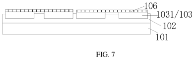
- FIG. 7 is a cross-sectional schematic diagram of solder strips, cells, and a first adhesive layer according to embodiments of the disclosure.
- embodiments of the disclosure provide a photovoltaic module, which is manufactured by the method for manufacturing the photovoltaic module described above.
- the photovoltaic module includes a front plate 101, a first adhesive layer 102, a plurality of cell strings 103, a second adhesive layer 104, and a back plate 105 that are arranged sequentially.
- Each cell string 103 includes a plurality of cells 1031, and each two adjacent cells are connected through a plurality of solder strips 106.
- the front plate 101 can be tempered glass, and the tempered glass has the advantages of high strength, high bending strength, high impact strength, and good safety performance.
- the back plate 105 can be a polyvinyl fluoride composite film photovoltaic back plate, which is commonly known as a TPT photovoltaic back plate.
- the TPT photovoltaic back plate has the characteristics of good weather resistance, aging resistance, tear resistance, good air isolation effect, and good insulation.
- the first adhesive layer 102 and/or the second adhesive layer 104 are glue or adhesive films.
- a respective cell is a back-contact cell, and solder strips (not shown) are connected to the back of the cells.
- a thickness of the glue or the adhesive film between the front plate and the plurality of cell strings in a direction perpendicular to a surface of the photovoltaic module ranges from 150 ⁇ m to 250 ⁇ m.
- the thickness of the glue or the adhesive film between the front plate and the plurality of cell strings is less than 150 ⁇ m in the direction perpendicular to the surface of the photovoltaic module, the cell is easy to directly contact the front plate, the cell is prone to breakage. If the thickness of the glue or the adhesive film between the front plate and the plurality of cell strings is greater than 250 ⁇ m in the direction perpendicular to the surface of the photovoltaic module, the cost of the photovoltaic module is higher.
- the thickness of the glue or the adhesive film between the front plate and the plurality of cell strings ranges from 150 ⁇ m to 250 ⁇ m, which can not only avoid the risk of breakage of the cells, but also help to reduce the cost of the photovoltaic module.
- the first adhesive layer is glue or an adhesive film
- the thickness of the glue or the adhesive film between the front plate and the plurality of cell strings in the direction perpendicular to the surface of the photovoltaic module can be 150 ⁇ m, 180 ⁇ m, 210 ⁇ m, or 250 ⁇ m.
- a thickness of the glue between the back plate and the plurality of cell strings in the direction perpendicular to the surface of the photovoltaic module ranges from 200 ⁇ m to 300 ⁇ m.
- the thickness of the glue between the back plate and the plurality of cell strings in the direction perpendicular to the surface of the photovoltaic module is less than 200 ⁇ m, the cell 1031 is easy to contact the back plate 105 directly, and the cell 1031 is easy to break. If the thickness of the glue between the back plate and the plurality of cell strings in the direction perpendicular to the surface of the photovoltaic module is greater than 300 ⁇ m, the cost of the photovoltaic module is higher.
- the thickness of the glue between the back plate and the plurality of cell strings in the direction perpendicular to the surface of the photovoltaic module ranges from 200 ⁇ m to 300 ⁇ m, which can not only avoid the risk of breakage of the cells, but also help to reduce the cost of the photovoltaic module.
- the thickness of the glue between the back plate and the plurality of cell strings in the direction perpendicular to the surface of the photovoltaic module can be 200 ⁇ m, 220 ⁇ m, 240 ⁇ m, 260 ⁇ m, 280 ⁇ m, or 300 ⁇ m.
- a thickness of the adhesive film between the back plate and the plurality of cell strings in the direction perpendicular to the surface of the photovoltaic module ranges from 300 ⁇ m to 450 ⁇ m.
- the thickness of the adhesive film between the back plate and the plurality of cell strings is less than 300 ⁇ m in the direction perpendicular to the surface of the photovoltaic module, the cell 1031 is easy to directly contact the back plate 105, and the cell 1031 is easy to break. If the thickness of the adhesive film between the back plate and the plurality of cell strings is greater than 450 ⁇ m in the direction perpendicular to the surface of the photovoltaic module, the cost of the photovoltaic module is too high.
- the thickness of the adhesive film between the back plate and the plurality of cell strings in the direction perpendicular to the surface of the photovoltaic module is designed to be in the range of 300 ⁇ m to 450 ⁇ m, which can not only avoid the risk of breakage of the cells, but also help to reduce the cost of the photovoltaic module.
- the thickness of the adhesive film between the back plate and the plurality of cell strings in the direction perpendicular to the surface of the photovoltaic module may be 300 ⁇ m, 330 ⁇ m, 360 ⁇ m, 390 ⁇ m, or 450 ⁇ m.
- a thickness of the back-contact cell in the direction perpendicular to a surface of the photovoltaic module is in a range of 100 ⁇ m to 200 ⁇ m.
- glue Before curing the glue between the front plate and the plurality of cells, at least half of the thickness of the cell should be covered with glue. For example, a thickness of the glue that goes over the cell accounts for 1/2 to 3/4 of the thickness of the cell.
- the photovoltaic module provided in the embodiments at least realizes the following beneficial effects.
- the photovoltaic module provided in the embodiments is manufactured by the method for manufacturing the photovoltaic module described above, and can prevent the cells from warping due to stress caused by single-side welding by pre-curing the glue and/or the encapsulation adhesive film between the front plate and the plurality of cells, thereby avoiding the risk of cracking and fragmentation of the cells, further improving the yield of the photovoltaic module and reducing the manufacturing cost.
- an area of the glue between the front/back plate and the plurality of cell strings is greater than or equal to a total area of the plurality of cell strings, and/or a size of the adhesive film between the front/back plate and the plurality of cell strings is greater than or equal to the total area of the plurality of cell strings.
- the area of the glue and/or the size of the adhesive film is greater than or equal to that of the plurality of cell strings, which is more beneficial to the encapsulation of the photovoltaic module.
- parts such as a layer, a film, a region, or a plate
- it may be “directly on” another part or may have another part present therebetween.
- a part of a layer, film, region, plate, etc. is “directly on” another part, it means that no other part is positioned therebetween.
Landscapes
- Photovoltaic Devices (AREA)
Applications Claiming Priority (1)
| Application Number | Priority Date | Filing Date | Title |
|---|---|---|---|
| CN202211481197.6A CN115588716B (zh) | 2022-11-24 | 2022-11-24 | 光伏组件的制造方法和光伏组件 |
Publications (3)
| Publication Number | Publication Date |
|---|---|
| EP4376101A1 true EP4376101A1 (fr) | 2024-05-29 |
| EP4376101B1 EP4376101B1 (fr) | 2026-03-04 |
| EP4376101C0 EP4376101C0 (fr) | 2026-03-04 |
Family
ID=84783559
Family Applications (1)
| Application Number | Title | Priority Date | Filing Date |
|---|---|---|---|
| EP23205211.8A Active EP4376101B1 (fr) | 2022-11-24 | 2023-10-23 | Procédé de fabrication de module photovoltaïque |
Country Status (5)
| Country | Link |
|---|---|
| US (1) | US12119420B2 (fr) |
| EP (1) | EP4376101B1 (fr) |
| JP (1) | JP2024076350A (fr) |
| CN (1) | CN115588716B (fr) |
| AU (1) | AU2023254905B2 (fr) |
Families Citing this family (5)
| Publication number | Priority date | Publication date | Assignee | Title |
|---|---|---|---|---|
| CN116845123B (zh) * | 2023-07-03 | 2024-02-02 | 无锡荷雨新能源科技有限公司 | 一种光伏组件及其制备工装与制备方法 |
| CN116995109A (zh) * | 2023-08-29 | 2023-11-03 | 正泰新能科技有限公司 | 一种低温焊接的背接触光伏组件及其制备方法 |
| CN116914034A (zh) * | 2023-09-13 | 2023-10-20 | 浙江晶科能源有限公司 | 光伏组件及其制备方法 |
| CN119153577A (zh) * | 2024-08-29 | 2024-12-17 | 滁州捷泰新能源科技有限公司 | 一种背接触电池串的敷设方法 |
| CN119584688B (zh) * | 2024-12-04 | 2025-11-07 | 晶科能源股份有限公司 | 一种光伏组件的制备方法及光伏组件 |
Citations (4)
| Publication number | Priority date | Publication date | Assignee | Title |
|---|---|---|---|---|
| DE102007035883A1 (de) * | 2007-07-31 | 2009-02-12 | Institut Für Solarenergieforschung Gmbh | Rückkontaktsolarzelle und Solarmodul mit reduzierten Serienwiderständen |
| US20120298172A1 (en) * | 2009-11-30 | 2012-11-29 | Imec | Method for manufacturing photovoltaic modules comprising back-contact cells |
| EP2575184A2 (fr) * | 2011-09-29 | 2013-04-03 | LG Electronics Inc. | Module de cellule solaire |
| CN107492581A (zh) * | 2017-08-04 | 2017-12-19 | 中来光伏科技(扬州)有限公司 | 背接触式太阳能电池组件及其制造方法 |
Family Cites Families (20)
| Publication number | Priority date | Publication date | Assignee | Title |
|---|---|---|---|---|
| US20090101197A1 (en) * | 2005-05-11 | 2009-04-23 | Mitsubishi Electric Corporation | Solar Battery and Production Method Thereof |
| DE102010027747A1 (de) | 2010-04-14 | 2011-10-20 | Robert Bosch Gmbh | Verfahren zur Herstellung eines Photovoltaikmoduls mit rückseitenkontaktierten Halbleiterzellen und Photovoltaikmodul |
| JP2012094742A (ja) * | 2010-10-28 | 2012-05-17 | Fujifilm Corp | 太陽電池モジュールおよびその製造方法 |
| WO2012058053A2 (fr) | 2010-10-29 | 2012-05-03 | Applied Materials, Inc. | Ensemble module monolithique utilisant des cellules solaires à contact arrière et du ruban métallique |
| CN102738310A (zh) * | 2012-07-16 | 2012-10-17 | 中电电气(南京)光伏有限公司 | 减少封装胶膜互融混色的晶硅光伏组件的封装方法 |
| US9666739B2 (en) | 2013-06-28 | 2017-05-30 | Sunpower Corporation | Photovoltaic cell and laminate metallization |
| NL2012557B1 (en) | 2014-04-02 | 2016-02-15 | Stichting Energieonderzoek Centrum Nederland | Photovoltaic module. |
| CN104752560B (zh) | 2015-03-03 | 2017-01-25 | 晶澳(扬州)太阳能科技有限公司 | 一种背接触太阳能电池组件的制作方法 |
| WO2017043518A1 (fr) | 2015-09-08 | 2017-03-16 | デクセリアルズ株式会社 | Procédé de fabrication de module de batterie solaire, module de batterie solaire, et procédé de connexion de cellules de batterie solaire |
| US9978896B2 (en) * | 2015-09-15 | 2018-05-22 | Sunpower Corporation | Encapsulant bonding methods for photovoltaic module manufacturing |
| JP7337838B2 (ja) | 2018-11-13 | 2023-09-04 | 株式会社カネカ | 太陽電池モジュールの製造方法 |
| CN111863991A (zh) * | 2019-04-23 | 2020-10-30 | 泰州隆基乐叶光伏科技有限公司 | 光伏组件及其制备方法 |
| JP6924887B1 (ja) | 2020-11-02 | 2021-08-25 | ジョジアン ジンコ ソーラー カンパニー リミテッド | 光起電力モジュール |
| CN112968075B (zh) * | 2021-02-02 | 2023-05-23 | 晶澳(扬州)新能源有限公司 | 一种光伏组件制作方法 |
| CN113066885B (zh) * | 2021-03-18 | 2023-07-14 | 苏州沃特维自动化系统有限公司 | 一种串联光伏电池组件及其封装方法 |
| CN113314637A (zh) | 2021-05-28 | 2021-08-27 | 宁夏小牛自动化设备有限公司 | 一种单面焊接的密栅太阳能电池串的制备方法 |
| CN215418196U (zh) * | 2021-07-29 | 2022-01-04 | 苏州福斯特光伏材料有限公司 | 光伏组件 |
| CN113611763A (zh) * | 2021-08-02 | 2021-11-05 | 上海晶澳太阳能科技有限公司 | 一种光伏组件及其制备方法 |
| CN114899274A (zh) | 2022-04-13 | 2022-08-12 | 高瑞 | 光伏组件薄片电池片的批量串联加工工艺 |
| CN217485460U (zh) * | 2022-04-18 | 2022-09-23 | 杭州福斯特应用材料股份有限公司 | 一种光伏组件 |
-
2022
- 2022-11-24 CN CN202211481197.6A patent/CN115588716B/zh active Active
-
2023
- 2023-10-19 US US18/490,663 patent/US12119420B2/en active Active
- 2023-10-23 EP EP23205211.8A patent/EP4376101B1/fr active Active
- 2023-10-24 JP JP2023182728A patent/JP2024076350A/ja active Pending
- 2023-10-24 AU AU2023254905A patent/AU2023254905B2/en active Active
Patent Citations (4)
| Publication number | Priority date | Publication date | Assignee | Title |
|---|---|---|---|---|
| DE102007035883A1 (de) * | 2007-07-31 | 2009-02-12 | Institut Für Solarenergieforschung Gmbh | Rückkontaktsolarzelle und Solarmodul mit reduzierten Serienwiderständen |
| US20120298172A1 (en) * | 2009-11-30 | 2012-11-29 | Imec | Method for manufacturing photovoltaic modules comprising back-contact cells |
| EP2575184A2 (fr) * | 2011-09-29 | 2013-04-03 | LG Electronics Inc. | Module de cellule solaire |
| CN107492581A (zh) * | 2017-08-04 | 2017-12-19 | 中来光伏科技(扬州)有限公司 | 背接触式太阳能电池组件及其制造方法 |
Non-Patent Citations (6)
| Title |
|---|
| AGROUI K ET AL: "Thermal stability of slow and fast cure EVA encapsulant material for photovoltaic module manufacturing process", SOLAR ENERGY MATERIALS AND SOLAR CELLS, ELSEVIER SCIENCE PUBLISHERS, AMSTERDAM, NL, vol. 90, no. 15, 22 September 2006 (2006-09-22), pages 2509 - 2514, XP028002407, ISSN: 0927-0248, [retrieved on 20060922], DOI: 10.1016/J.SOLMAT.2006.03.023 * |
| GALICA J P ET AL: "Development of low cost faster-curing encapsulants for terrestrial PV modules", PROC. OF THE 16TH EU-PVSEC, 1 May 2000 (2000-05-01) - 5 May 2000 (2000-05-05), pages 1 - 4, XP093138101 * |
| GOVAERTS J. ET AL: "A Novel Concept for Advanced Modules with Back-Contact Solar Cells", 25TH EUPVSEC, 6 September 2010 (2010-09-06), pages 3850 - 3853, XP093137030, DOI: 10.4229/25theupvsec2010-4co.19.4 * |
| JIANG SHAN ET AL: "Encapsulation of PV Modules Using Ethylene Vinyl Acetate Copolymer as the Encapsulant", MACROMOLECULAR REACTION ENGINEERING, vol. 9, no. 5, 27 March 2015 (2015-03-27), Hoboken, USA, pages 522 - 529, XP093137020, ISSN: 1862-832X, DOI: 10.1002/mren.201400065 * |
| JONATHAN GOVAERTS ET AL: "The i-module approach: Towards improved performance and reliability of photovoltaic modules", MICROELECTRONICS AND PACKAGING CONFERENCE (EMPC), 2011 18TH EUROPEAN, IEEE, 12 September 2011 (2011-09-12), pages 1 - 5, XP032106495, ISBN: 978-1-4673-0694-2 * |
| MARC K�NTGES ET AL: "A novel photovoltaic-module assembly system for back contact solar cells using laser soldering technique", PROC. OF THE 23RD EUROPEAN PHOTOVOLTAIC SOLAR ENERGY CONFERENCE, 1 September 2008 (2008-09-01) - 5 September 2008 (2008-09-05), pages 2709 - 2712, XP040529473, ISBN: 978-3-936338-24-9 * |
Also Published As
| Publication number | Publication date |
|---|---|
| AU2023254905B2 (en) | 2025-08-28 |
| US20240178334A1 (en) | 2024-05-30 |
| CN115588716B (zh) | 2023-04-07 |
| JP2024076350A (ja) | 2024-06-05 |
| AU2023254905A1 (en) | 2024-06-13 |
| EP4376101B1 (fr) | 2026-03-04 |
| US12119420B2 (en) | 2024-10-15 |
| CN115588716A (zh) | 2023-01-10 |
| EP4376101C0 (fr) | 2026-03-04 |
Similar Documents
| Publication | Publication Date | Title |
|---|---|---|
| EP4376101A1 (fr) | Procédé de fabrication de module photovoltaïque et module photovoltaïque | |
| CN113066885B (zh) | 一种串联光伏电池组件及其封装方法 | |
| CN101685838B (zh) | 一种光伏组件及其制造方法 | |
| EP4521470B1 (fr) | Procédé de fabrication de module photovoltaïque et module photovoltaïque | |
| KR102790452B1 (ko) | Bipv 적용 가능한 고출력 슁글드 태양광 모듈 및 그 제조 방법 | |
| EP1921684A1 (fr) | Module de cellule solaire et son procédé de fabrication | |
| CN116995109A (zh) | 一种低温焊接的背接触光伏组件及其制备方法 | |
| US12484334B2 (en) | Photovoltaic cell module and manufacturing method thereof | |
| CN118888645B (zh) | 光伏组件及其制备方法 | |
| AU2024393997A1 (en) | Photovoltaic cell string, photovoltaic cell panel and photovoltaic cell module | |
| KR20240159419A (ko) | 태양광 모듈 및 태양광 모듈의 제조 방법 | |
| WO2025055503A1 (fr) | Module photovoltaïque et système photovoltaïque | |
| CN116914034A (zh) | 光伏组件及其制备方法 | |
| CN104900756A (zh) | 一种薄膜光伏组件层压工艺 | |
| JP2001244486A (ja) | 太陽電池モジュール | |
| CN111370517A (zh) | 一种光伏盖板及光伏组件 | |
| CN211238270U (zh) | 光伏组件 | |
| CN220306259U (zh) | 一种电池片及光伏组件 | |
| CN117012849A (zh) | 自由曲面高效太阳能电池光伏组件的制作方法 | |
| CN115763601A (zh) | 一种使用磁性贴作为背面封装材料的车用光伏组件 | |
| CN212967722U (zh) | 光伏组件用封装胶膜和具有其的光伏组件 | |
| CN113421938A (zh) | 一种太阳能电池模组、高效叠层曲面光伏瓦及其制备方法 | |
| CN218215329U (zh) | 一种叠瓦集热光伏组件 | |
| CN223515240U (zh) | 一种电池组件、电池串以及光伏系统 | |
| EP2383796A1 (fr) | Module de cellules solaires |
Legal Events
| Date | Code | Title | Description |
|---|---|---|---|
| PUAI | Public reference made under article 153(3) epc to a published international application that has entered the european phase |
Free format text: ORIGINAL CODE: 0009012 |
|
| STAA | Information on the status of an ep patent application or granted ep patent |
Free format text: STATUS: REQUEST FOR EXAMINATION WAS MADE |
|
| 17P | Request for examination filed |
Effective date: 20231024 |
|
| AK | Designated contracting states |
Kind code of ref document: A1 Designated state(s): AL AT BE BG CH CY CZ DE DK EE ES FI FR GB GR HR HU IE IS IT LI LT LU LV MC ME MK MT NL NO PL PT RO RS SE SI SK SM TR |
|
| STAA | Information on the status of an ep patent application or granted ep patent |
Free format text: STATUS: EXAMINATION IS IN PROGRESS |
|
| 17Q | First examination report despatched |
Effective date: 20250328 |
|
| REG | Reference to a national code |
Ref country code: DE Ref legal event code: R079 Free format text: PREVIOUS MAIN CLASS: H01L0031050000 Ref country code: DE Ref legal event code: R079 Ref document number: 602023012928 Country of ref document: DE Free format text: PREVIOUS MAIN CLASS: H01L0031050000 Ipc: H10F0019800000 |
|
| GRAP | Despatch of communication of intention to grant a patent |
Free format text: ORIGINAL CODE: EPIDOSNIGR1 |
|
| STAA | Information on the status of an ep patent application or granted ep patent |
Free format text: STATUS: GRANT OF PATENT IS INTENDED |
|
| RIC1 | Information provided on ipc code assigned before grant |
Ipc: H10F 19/80 20250101AFI20251024BHEP Ipc: H10F 19/85 20250101ALI20251024BHEP Ipc: H10F 19/90 20250101ALI20251024BHEP |
|
| INTG | Intention to grant announced |
Effective date: 20251110 |
|
| GRAS | Grant fee paid |
Free format text: ORIGINAL CODE: EPIDOSNIGR3 |
|
| GRAA | (expected) grant |
Free format text: ORIGINAL CODE: 0009210 |
|
| STAA | Information on the status of an ep patent application or granted ep patent |
Free format text: STATUS: THE PATENT HAS BEEN GRANTED |
|
| AK | Designated contracting states |
Kind code of ref document: B1 Designated state(s): AL AT BE BG CH CY CZ DE DK EE ES FI FR GB GR HR HU IE IS IT LI LT LU LV MC ME MK MT NL NO PL PT RO RS SE SI SK SM TR |
|
| REG | Reference to a national code |
Ref country code: CH Ref legal event code: F10 Free format text: ST27 STATUS EVENT CODE: U-0-0-F10-F00 (AS PROVIDED BY THE NATIONAL OFFICE) Effective date: 20260304 Ref country code: GB Ref legal event code: FG4D |
|
| REG | Reference to a national code |
Ref country code: IE Ref legal event code: FG4D |
|
| REG | Reference to a national code |
Ref country code: DE Ref legal event code: R096 Ref document number: 602023012928 Country of ref document: DE |
|
| U01 | Request for unitary effect filed |
Effective date: 20260305 |
|
| U07 | Unitary effect registered |
Designated state(s): AT BE BG DE DK EE FI FR IT LT LU LV MT NL PT RO SE SI Effective date: 20260311 |