EP4379352A1 - Photoakustisches system und verfahren dafür - Google Patents
Photoakustisches system und verfahren dafür Download PDFInfo
- Publication number
- EP4379352A1 EP4379352A1 EP23212493.3A EP23212493A EP4379352A1 EP 4379352 A1 EP4379352 A1 EP 4379352A1 EP 23212493 A EP23212493 A EP 23212493A EP 4379352 A1 EP4379352 A1 EP 4379352A1
- Authority
- EP
- European Patent Office
- Prior art keywords
- face
- diffraction grating
- waveguide
- window
- semiconductor substrate
- Prior art date
- Legal status (The legal status is an assumption and is not a legal conclusion. Google has not performed a legal analysis and makes no representation as to the accuracy of the status listed.)
- Pending
Links
Images




Classifications
-
- H—ELECTRICITY
- H01—ELECTRIC ELEMENTS
- H01S—DEVICES USING THE PROCESS OF LIGHT AMPLIFICATION BY STIMULATED EMISSION OF RADIATION [LASER] TO AMPLIFY OR GENERATE LIGHT; DEVICES USING STIMULATED EMISSION OF ELECTROMAGNETIC RADIATION IN WAVE RANGES OTHER THAN OPTICAL
- H01S3/00—Lasers, i.e. devices using stimulated emission of electromagnetic radiation in the infrared, visible or ultraviolet wave range
- H01S3/05—Construction or shape of optical resonators; Accommodation of active medium therein; Shape of active medium
- H01S3/06—Construction or shape of active medium
- H01S3/063—Waveguide lasers, i.e. whereby the dimensions of the waveguide are of the order of the light wavelength
- H01S3/0632—Thin film lasers in which light propagates in the plane of the thin film
- H01S3/0635—Thin film lasers in which light propagates in the plane of the thin film provided with a periodic structure, e.g. using distributed feed-back, grating couplers
-
- G—PHYSICS
- G01—MEASURING; TESTING
- G01N—INVESTIGATING OR ANALYSING MATERIALS BY DETERMINING THEIR CHEMICAL OR PHYSICAL PROPERTIES
- G01N21/00—Investigating or analysing materials by the use of optical means, i.e. using sub-millimetre waves, infrared, visible or ultraviolet light
- G01N21/17—Systems in which incident light is modified in accordance with the properties of the material investigated
- G01N21/1702—Systems in which incident light is modified in accordance with the properties of the material investigated with opto-acoustic detection, e.g. for gases or analysing solids
-
- G—PHYSICS
- G01—MEASURING; TESTING
- G01N—INVESTIGATING OR ANALYSING MATERIALS BY DETERMINING THEIR CHEMICAL OR PHYSICAL PROPERTIES
- G01N29/00—Investigating or analysing materials by the use of ultrasonic, sonic or infrasonic waves; Visualisation of the interior of objects by transmitting ultrasonic or sonic waves through the object
- G01N29/22—Details, e.g. general constructional or apparatus details
- G01N29/24—Probes
- G01N29/2418—Probes using optoacoustic interaction with the material, e.g. laser radiation, photoacoustics
-
- H—ELECTRICITY
- H01—ELECTRIC ELEMENTS
- H01S—DEVICES USING THE PROCESS OF LIGHT AMPLIFICATION BY STIMULATED EMISSION OF RADIATION [LASER] TO AMPLIFY OR GENERATE LIGHT; DEVICES USING STIMULATED EMISSION OF ELECTROMAGNETIC RADIATION IN WAVE RANGES OTHER THAN OPTICAL
- H01S3/00—Lasers, i.e. devices using stimulated emission of electromagnetic radiation in the infrared, visible or ultraviolet wave range
- H01S3/05—Construction or shape of optical resonators; Accommodation of active medium therein; Shape of active medium
- H01S3/08—Construction or shape of optical resonators or components thereof
- H01S3/08004—Construction or shape of optical resonators or components thereof incorporating a dispersive element, e.g. a prism for wavelength selection
- H01S3/08009—Construction or shape of optical resonators or components thereof incorporating a dispersive element, e.g. a prism for wavelength selection using a diffraction grating
-
- G—PHYSICS
- G01—MEASURING; TESTING
- G01N—INVESTIGATING OR ANALYSING MATERIALS BY DETERMINING THEIR CHEMICAL OR PHYSICAL PROPERTIES
- G01N21/00—Investigating or analysing materials by the use of optical means, i.e. using sub-millimetre waves, infrared, visible or ultraviolet light
- G01N21/17—Systems in which incident light is modified in accordance with the properties of the material investigated
- G01N21/1702—Systems in which incident light is modified in accordance with the properties of the material investigated with opto-acoustic detection, e.g. for gases or analysing solids
- G01N2021/1704—Systems in which incident light is modified in accordance with the properties of the material investigated with opto-acoustic detection, e.g. for gases or analysing solids in gases
Definitions
- the technical field of the invention is that of photoacoustic systems, for example, used in the detection of chemical compounds in a gas or in a vascularized skin sample.
- Photoacoustic detection systems make it possible to detect and quantify target species present in a continuous medium such as a gas or a liquid.
- Photoacoustic detection systems rely on the emission of an acoustic wave in the continuous medium in response to selective excitation of target atoms or target molecules in this continuous medium by means of a light beam.
- the acoustic wave, captured by a microphone, is proportional to the density of target atoms or target molecules in the continuous medium.
- the document [“ Downsizing and Silicon Integration of Photoacoustic Gas Cells » Glière et al., International Journal of Thermophysics (2020) 41:16 ] discloses a detection system comprising a volume intended to accommodate the continuous medium.
- the disclosed system is, however, notable in that the volume is restricted.
- the photoacoustic signal is inversely proportional to the volume of the continuous medium in which the acoustic wave propagates.
- a direct way to improve the resolution of a detection system therefore consists of reducing the volume involved, ideally within the limit of a few cubic micrometers for a measurement at atmospheric pressure (otherwise the volume is too low than the probability of interaction of a photon with a gas molecule is sufficient).
- the disclosed system takes advantage of Si device manufacturing methods that allow very small hollow volumes to be formed within a silicon substrate itself. It is notably disclosed to etch a network of trenches on the surface of two distinct substrates. The two substrates are then glued to each other so that the trench networks are facing each other. The two distinct substrates thus form a thick substrate and the two trench networks form a hollow volume in the volume of the thick substrate, under the surfaces of said thick substrate.
- the disclosed hollow volume comprises a main, rectilinear cavity and a transparent window arranged on a slice of the thick substrate. A light beam aligned with the window (we then speak of abutment) can then enter the main cavity and interact with the medium present in the cavity. Thus, a laser beam correctly aligned with the first cavity can interact with the continuous medium present in the main cavity and induce a photoacoustic response in the medium.
- the window has a transmission coefficient greater than 50%, in other words, at least 50% of the power conveyed by the electromagnetic field is transmitted by the window.
- the diffraction grating has a diffraction order greater than or equal to two makes it possible to extract the electromagnetic field generated by the active region.
- the diffraction grating notably allows a component of the field to propagate out of the plane. A substantial part of the power carried by the out-of-plane component (which we will call electromagnetic radiation) is then emitted by the second face of the waveguide.
- the electromagnetic radiation, coming from the surface emission device is injected directly into the hollow volume. It can therefore be implemented to carry out a photoacoustic measurement.
- a surface emitting device emits electromagnetic radiation that exhibits good near-field homogeneity and low angular dispersion. Therefore, a continuous medium in the hollow volume directly above the surface emission device (and more particularly directly above the window) can be excited effectively by the radiation coming from the surface emission device.
- the limited thickness of the window also helps reduce radiation absorption.
- the surface emission device can be placed as close as possible to the window (or even on the window) and therefore as close as possible to the hollow volume, so as to effectively illuminate a medium which is in the hollow volume.
- the photoacoustic system according to the invention is therefore efficient.
- the surface emitting device extends on the upper face of the substrate and not near a slice of the substrate also simplifies its integration into the photoacoustic system. Just drop it (or make it) on the window.
- the sources of uncertainty regarding the alignment are weak. Indeed, the surface emission device being deposited on the upper face (or on an optical sole which is itself deposited on the upper face), the uncertainty on its distance or its inclination relative to the upper face is low. or even negligible.
- rotating the device along an axis perpendicular to the window does not necessarily produce any effect.
- the alignment constraint is therefore relaxed compared to a system according to the prior art.
- the window can be widened as much as necessary to absorb an alignment error of the device relative to the latter.
- the measurement or detection results that can be obtained with several photoacoustic systems according to the invention are therefore reproducible.
- the surface emitting device can have reduced dimensions, making it a good candidate for integration into a lab-on-a-chip.
- the dimensions, particularly lateral, of the surface emitting device can be reduced as much as necessary, to further reduce its size and the size of the photoacoustic system.
- the photoacoustic system according to the invention is therefore easily integrable, for example in a laboratory on a chip.
- the diffraction grating of said at least one device extends over the first face of the waveguide of said at least one device and said diffraction grating is reflective.
- the diffraction grating of said at least one device comprises a periodic structure and a metallic layer, the periodic structure extending over the first face of the waveguide and the metallic layer extending over the periodic structure.
- the diffraction grating of said at least one device extends over the second face of the waveguide of said at least one device and said diffraction grating is non-reflective.
- the periodic structure of the diffraction grating of said at least one device comprises an alternation of first portions and second portions, the first portions being made up of a first semiconductor material having a first optical index and the second portions being made up of a metal or a second material, such as another semiconductor material or a gas, having a second optical index different from the first optical index.
- the diffraction grating of said at least one device extends directly above the active region of the waveguide of said at least one device, the active region having a length, measured in the first direction, and the grating of diffraction of said at least one device having a length, also measured in the first direction, the length of said diffraction grating being substantially equal to the length of said active region, said grating presenting, in the first direction, a single diffraction order.
- the diffraction grating of said at least one device has, in the first direction, a diffraction order greater than or equal to three.
- the active region of said at least one device has a width, measured in a second direction, parallel to the emitting face of said at least one device and perpendicular to the first direction
- the diffraction grating of said at least one device has a width , measured in the second direction, the width of said diffraction grating being substantially equal to the width of said active region, said diffraction grating presenting, in the second direction, another diffraction order, unique and greater than or equal to two.
- the waveguide of said at least one device is delimited by a first flank and a second flank, the second flank being opposite the first flank, the first and second flanks being substantially perpendicular to the second face, said device also comprising a first conductive layer and a second conductive layer, the first conductive layer extending on the first side and the second conductive layer extending on the second side.
- said at least one surface emitting device is glued to the window and preferably by molecular bonding or by means of a polymerizable glue.
- said at least one surface emission device is configured to emit infrared electromagnetic radiation through its emitting face with an angle, measured relative to the normal of said emitting face, of between 0° and 60°.
- the semiconductor substrate comprises a plurality of windows and the photoacoustic system comprises a plurality of surface emitting devices, each surface emitting device of the plurality of surface emitting devices being arranged on a window of the plurality of windows.
- the electromagnetic radiation comprises a wavelength of [0.8 ⁇ m; 20 ⁇ m] and preferably in [4 ⁇ m; 12 ⁇ m].
- the photoacoustic system comprises a thermal regulator configured to regulate the temperature of said at least one surface emitting device.
- the thermal regulator configured to regulate the temperature of said at least one surface emission device when said at least one surface emission device operates in a stationary regime.
- the thermal regulator is configured to regulate the temperature of said at least one surface emitting device to within 0.1°C.
- the thermal regulator is configured to regulate the temporal variation of the temperature of said at least one surface emitting device to within less than 0.1°C/s.
- FIG. 2 schematically shows an embodiment of a surface emission device that can be implemented in the photoacoustic system according to the invention.
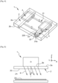
- FIG. 1a and [Fig. 1b ] schematically show an embodiment of a photoacoustic system 1 according to the invention.
- the system 1 is adapted to measure a concentration of a targeted species in a gas.
- System 1 is based on the measurement of a sound wave resulting from photoacoustic emission by the targeted species in the gas.
- the system 1 notably comprises a surface emission device 3, two sound sensors 4 (in other words microphones) and a Helmholtz resonator 21 into which the gas comprising the targeted species can be introduced.
- the surface emission device 3 is coupled to the Helmholtz resonator so as to inject electromagnetic radiation which can excite the targeted species in the gas.
- the sound sensors 4 are coupled to the resonator 21 in order to measure the amplitude of the sound waves propagating in the resonator 21 and resulting from the photoacoustic emission by the targeted species.
- System 1 illustrated in [ Fig. 1a] and [Fig. 1b ] is partially truncated, in two different configurations, to show the elements of system 1.
- the system 1 as illustrated comprises a semiconductor substrate 2 comprising the resonator 21.
- the substrate 2 extends in a plane ⁇ X; Y ⁇ formed by a first direction X and a second direction Y, orthogonal to the first direction X.
- the substrate 2 comprises two large faces 2a, 2b, opposite each other. That is to say a face 2a called “upper face”, oriented in a third direction Z, and a face 2b called “lower face”, oriented in the third direction -Z and opposite to the upper face 2a.
- the two large faces 2a, 2b are delimited by a side 2c (also called “edge”), forming the perimeter of the substrate 2.
- the substrate 2 may have a thickness W 2 , measured in the Z direction, comprised in [0.5 mm; 3mm].
- the substrate 2 may have a length L 2 and a width l 2 , respectively measured along the first and second directions X and Y, included in [5 mm; 20mm].
- the resonator 21 comprises two hollow volumes 21a, 21b which will also be called “main cavities”.
- the main cavities 21a, 21b extend parallel to each other along X. They extend in the volume of the substrate 2, under the upper face 2a of the substrate 2. In other words, they extend distance from the upper face 2a.
- Each of the main cavities 21a, 21b is delimited by an internal wall in the substrate 2.
- the resonator 12 also includes channels 211 connecting the main cavities 21a, 21b.
- the channels 211 illustrated each have an opening 212, made in the upper face 2a of the substrate 2. These openings 212 can be used to introduce the gas and the targeted species into the resonator 21.
- the semiconductor substrate 2 can be formed from two assembled thin semiconductor substrates 2', 2".
- a line 20 illustrates for example the interface between the two assembled thin substrates 2', 2".
- each of the thin substrates 2', 2" is etched so as to form trenches which will make up the resonator 21.
- Substrate 2 is preferably made of Si.
- Substrate 2 comprises a portion 22 called a “window”.
- window we mean that it is adapted to transmit electromagnetic radiation into the resonator 21 and in particular into one of the main cavities 21a, 21b.
- the window 22 extends directly above at least part of one of the main cavities 21a, 21b.
- extending vertically we mean that the window is aligned with a portion of a cavity 21a, 21b in the direction Z (perpendicular to the upper face 2a).
- the window 22 extends into the substrate 2 and connects the upper surface 2a of the substrate 2 to one of the cavities 21a, 21b.
- the window 22 is therefore not an opening made in the substrate 2 so as to reveal a cavity 21a, 22b.
- the window 22 can be in the same material as the substrate 2, for example in Si.
- the transmission coefficient of the window 22 can vary as a function of the thickness W 22 of the window 22, measured in the direction Z.
- a Si window 22 is transparent to infrared radiation in a range [0.8 ⁇ m; 20 ⁇ m] when its thickness W 22 is less than or equal to 100 ⁇ m.
- a lower window thickness W 22 for example less than or equal to 50 ⁇ m, may be favored to further improve the transmission of infrared radiation.
- the window can also be made of another material, in particular when this has better transmission of electromagnetic radiation for certain wavelengths. For example, it may be a portion made of silicon nitride or silicon carbide.
- the window 22 is associated with a cavity 21a of the resonator 21.
- the substrate 2 may comprise a plurality of windows associated with a cavity.
- the windows extend from the upper face 2a of the substrate 2 to the same cavity 21a, but to different portions of said cavity 21a.
- the system 1 can include several surface emitting devices 3, each being arranged on one of the windows.
- the plurality of devices is coupled to the same cavity. This can be useful for exposing the same cavity to radiation having different wavelengths (for example to detect different species).
- the surface emission device 3 makes it possible to inject electromagnetic radiation into the resonator 21 and in particular into the main cavity 21a, 21b with which the window 22 is associated.
- surface emitting device we mean an electro-optical device configured to emit electromagnetic radiation through one of its faces, which is generally called the “emitting face”. It differs from an edge emission device for which the emission of electromagnetic radiation is carried out at an edge or a side of said device.
- a surface emitting device 3 it is possible to emit radiation in an out-of-plane direction. That is to say, in the case of [ Fig. 1a] and [Fig. 1b ], out of the plane ⁇ X; Y ⁇ . For example in the direction Z.
- the device 3 also makes it possible to emit radiation via a surface (the so-called “emitting” face) which has an area greater than an edge.
- the emitting face generally has a substantial area and makes it possible to obtain spatially homogeneous electromagnetic radiation, especially in the near field. It is therefore advantageous to use this type of device to inject electromagnetic radiation into the resonator 21 and effectively excite the targeted species in the gas.
- the device 3 is configured to transmit via a face 3b which we will call “transmitting face”.
- the electromagnetic radiation coming from the emitting face 3b is substantially perpendicular to the emitting face 3b.
- substantially perpendicular we mean that the radiation presents, with the emitting face 3b, an angle greater than or equal to 30° (that is to say between 30° and 90°).
- the surface emitting device 3 In order to inject electromagnetic radiation into the resonator 21 and in particular into the cavity 21a, the surface emitting device 3 is placed on the window 22. The emitting face 3b of the surface emitting device 3 is placed directly on the window contact 22a. In this way, the electromagnetic radiation emitted by the device 3 is directly transmitted to the cavity 21a. The emitted radiation can then excite the targeted species present in the resonator 21.
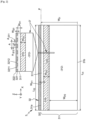
- FIG. 2 presents, in a sectional view, an embodiment of a surface emission device 3 which can be implemented in the photoacoustic system 1.
- the device 3 is represented in a section in the plane ⁇ X; Z ⁇ .
- There [ Fig. 2 ] also presents an enlargement of a portion 3' of said device 3, in the same plane.
- Device 3 comprises: a waveguide 31 and a diffraction grating 32.
- the waveguide 31 extends in a plane P which is for example parallel to the upper surface 2a of the system 1 (that is to say the plane ⁇ X; Y ⁇ ).
- the waveguide 31 comprises a first face 31a and a second face 31b, opposite the first face 31b.
- the first and second faces 31a, 31b extend parallel to the plane P.
- the first face 31a is for example oriented in the third direction Z, perpendicular to the plane P, and the second face 31b is oriented in the same direction but in one direction opposite.
- the waveguide 31 also includes an active region 310.
- the active region 310 is a portion of the waveguide 31 configured to emit an electromagnetic field (also called “electromagnetic radiation” or simply “field” or “radiation”).
- the active region 310 is for example configured so that the emission is spontaneous and/or stimulated. In the latter case, the active region could also be called “amplifying medium” because it can allow the device 3 to operate in laser mode.
- the active region 310 is for example a stack of sublayers, such as [InGaAs/AlInAs] ⁇ N, where N is the number of pairs of InGaAS/AlInAs sublayers, for example equal to one hundred. In this way, the active region 310 is configured to carry out spontaneous and stimulated emission.
- the active region may have a thickness W 310 , measured perpendicular to the plane P, which may be between 1 ⁇ m and 5 ⁇ m and preferably between 1.5 ⁇ m and 2.5 ⁇ m.
- the active region 310 is preferably framed by two semiconductor layers 311, 312, extending parallel to the plane P.
- the face of the upper coating 311 which is opposite the active region 310 is then advantageously the first face 31a.
- the face of the lower coating 312 which is opposite the active region 310 is then advantageously the second face 31b.
- the upper and lower coatings 311, 312 can allow the field to be guided in the waveguide 31.
- they advantageously have optical indices (also called refractive indices) strictly lower than the average optical index of the active region 310.
- the upper coating 311 has a thickness, measured perpendicular to the plane P, which can be between 1 ⁇ m and 2 ⁇ m.
- the lower coating 312 has a thickness, measured perpendicular to the plane P, which can be between 2 ⁇ m and 100 ⁇ m and preferably between 2 ⁇ m and 40 ⁇ m.
- the lower coating 312 is for example a semiconductor heterostructure of type III-V, that is to say materials classified in groups III B and V B of the periodic table of the elements (which, according to another convention, corresponds to columns 13 and 15 of the periodic table of elements).
- Said coating 312 is for example formed from InP.
- the lower coating 312 can also be doped, for example n-type, that is to say with impurities acting as electronic donors.
- the lower coating 312 is for example doped with S.
- the upper coating 311 can be, in the same way as the lower coating 312, a type III-V semiconductor heterostructure, such as InP. In the same way, the upper coating 311 can be doped, for example n-type.
- the waveguide 31 is therefore a stack of layers 310, 311, 312 extending parallel to the plane P. It can have the shape of a rectangular parallelepiped delimited from the sides. It has for example a length L 31 , a width and a thickness W 31 .
- the length of the waveguide 31 is for example measured in the first direction X.
- the width of the waveguide 31 is for example measured in the second direction Y, perpendicular to the first direction wave 31 is for example measured in the third direction Z, perpendicular to the two aforementioned directions X, Y.
- the length L 31 of the waveguide 31 can be between 1000 ⁇ m and 5000 ⁇ m. According to one embodiment, the length L 31 and the width of the waveguide 31 can be equal, for example to within 10%. Thus, seen from above, the first face 31a can have a square shape. Alternatively, the length L 31 of the waveguide 31 can be greater than the width of the waveguide 31 and for example greater than twice the width of the waveguide 31, or even greater than a hundred times the width of the guide d 'wave. In this case, we speak of a ridge type waveguide. For example, the width of the waveguide 31 (not shown in the figure) can be between 10 ⁇ m and 50 ⁇ m.
- the active region 310 has a length L 310 , measured in the first direction Y, substantially equal to the width of the waveguide 31. By substantially equal, we mean equal to within 20%, or even within 10%. Flanks, perpendicular to the plane P, delimit for example the waveguide 31 and the active region 310.
- the diffraction grating 32 extends over the first face 31a of the waveguide 31 and in particular over the upper coating 311.
- the emitting face 3b of the device 3 then coincides with the second face 31b of the waveguide.
- coincide we mean that the faces are coplanar.
- the diffraction grating is advantageously arranged directly above the active region 310 of the waveguide 31 and preferably centered relative to the latter.
- the diffraction grating 32 may have a length L 32 and a width.
- the length L 32 of the diffraction grating 32 is for example measured along the first direction X.
- the width of the diffraction grating 32 is for example measured along the second direction Y, perpendicular to the first direction of the diffraction grating 32 are advantageously chosen so that the diffraction grating 32 completely covers the active region 310.
- the lengths and widths of the diffraction grating 32 are, respectively, substantially equal to the lengths and widths of the diffraction grating 32. active region 310. In this way, the diffraction grating 32 can be coupled homogeneously to the field emitted by the active region 310. It makes it possible, for example, to provide a homogeneous distributed feedback over the entire length L 310 of the active region 310.
- the device 3 is remarkable on the one hand in that the second face 31b of the waveguide is transparent to the field which can be emitted by the active region 310.
- transparent we mean that the face 31b presents a spectral transmission window and that this transmission spectral window corresponds to at least part of the spectrum of the field which can be emitted by the active region 310.
- the second face 31b of the waveguide 31 also constitutes the emitting face 3b of the device 3.
- the device 3 is also remarkable in that the diffraction grating 32 is reflective and in that it has a diffraction order, in the first direction X, greater than or equal to two.
- reflective we mean that at least 50% of the field is reflected by the diffraction grating 32.
- the device 3 can therefore carry out transmission via the second face 31b.
- the second face 31b of the waveguide 31 therefore coincides with the emitting face 3b of the device 3.
- the diffraction grating 32 comprises a periodic structure 321.
- the periodic structure 321 is for example a layer extending over the first face 31a of the waveguide 31. Coupled with the field emitted by the active region 310, it induces diffraction effects.
- the coupling rate between the field and the diffraction grating 32 is advantageously between 10 cm -1 and 100 cm -1 .
- the periodic structure 321 comprises for example first portions 3211 and second portions 3212. These first and second portions 3211, 3212 are arranged periodically and form an alternation in the first direction X and in the second direction Y where appropriate.
- the first and second portions 3211, 3212 can be lines, oriented in the second direction Y. Said lines are arranged next to each other in the first direction alternation in the first direction X. In other words, they form two combs nested one inside the other.
- Fig. 2 illustrates this example.
- the first portions 3211 are pads arranged in a rectangular mesh.
- the second portions 3212 are tori surrounding each pad 3211 and filling the space between the pads 3211.
- the pads 3211 can have an elliptical shape, having a great length in the first direction a small length along the second direction Y or vice versa.
- the first portions 3211 are made of a first semiconductor material having a first optical index.
- the first semiconductor material is for example a type III-V semiconductor material, such as InP. It may also be the same material as the upper covering 311.
- the second portions 3212 are made of a second material or a metal.
- the second material may be another semiconductor material or a gas, such as air. In this case it has a second optical index different from the first optical index.
- the diffraction grating 32 advantageously presents, in the first direction X, a single diffraction order. That is to say that the period A (or “step”) with which the first portions 3211 are arranged is constant over the entire length L 32 of the network 12. The first portions 3211 then advantageously all have the same width A 3211 , measured in the first direction the period of the diffraction grating 32 in the first direction X is therefore equal to A 3211 + A 3212 .
- a single diffraction order means that the period A is constant, within +/- 10%, over the entire length L 32 of the diffraction grating.
- the active region 310 is preferably configured to emit in the infrared range, that is to say in a range [0.8 ⁇ m; 20 ⁇ m] or preferably [4 ⁇ m; 12 ⁇ m].
- Such wavelengths imply a period A of the network 12 of the order of a micrometer at least.
- a diffraction grating 32 applicable to the infrared spectrum is also simpler to produce than a grating presenting a much lower period (for example in the blue or ultraviolet spectrum).
- this type of range lends itself advantageously to photoacoustic measurement or detection.
- a large family of semiconductor materials is transparent to infrared radiation.
- the diffraction grating 32 also comprises a metallic layer 322 which extends over the periodic structure 321 and preferably over the entire periodic structure 321. It is for example made of Ti or Au.
- the reflective effect of the diffraction grating 32 can also be provided by the metal layer 322 extending over the periodic structure 321.
- the metal layer can prevent the transmission of the field through the diffraction grating 32.
- the metal layer 12 extends in particular over each first portion 3211 of the periodic structure 321. In this way it prevents the transmission of the field through the first portions 3211.
- the embodiment of the [ Fig. 2 ] illustrates a continuous metal layer 322 which extends in the first direction X.
- the metal layer 322 can be discontinuous and comprise a plurality of portions. Each portion therefore advantageously extends over each first portion 3211 of the periodic structure 3211. If for example the first portions 3211 of the structure of the periodic structure 321 are aligned in the second direction Y, then the metal layer 322 will comprise a plurality of portions also extending in the second direction Y, a portion of the metal layer extending over an upper surface of a first portion 3211.
- the metal layer 322 can also extend beyond the periodic structure 321 because it can also be used as a contact electrode of the device 3. It can make it possible to apply an electric field uniformly to the active region. 310 in order to inject carriers into the active region 310. The carriers can de-excite by emitting photons in the active region 310.
- the metal layer 322 also makes it possible to improve the confinement of the field in the waveguide 31 thanks to the plasmonic interaction of the field with the metal.
- the diffraction grating 32 can be configured so that it presents, in the second direction Y, perpendicular to the first direction X, an order greater than or equal to two also.
- the field propagating along the second direction Y also couples to the diffraction grating and induces a component of the field which also propagates outside the plane P, that is to say along +Z and/or -Z.
- This variant can be obtained when the first portions 3211 of the periodic structure 321 are pads arranged in a rectangular mesh.
- This variant is advantageous when the width and length of the active region (and therefore of the diffraction grating) are substantially equal, for example to within 20%.
- the length of the active region 310 is much greater than its width, for example 20 times greater than its width (“ridge” type guide), it is preferable that the diffraction grating 32 only presents an order according to the first direction
- the diffraction grating 32 can also present, along the second direction Y, a single diffraction order.
- the periods of arrangement of the first and second portions according to the first and second directions X and Y are then constant in the two directions. They can, however, be different, so that the order according to the first direction X is different from the order according to the second direction Y.
- the lateral confinement of the field can also be provided by conductive coatings extending on the sides of the waveguide 31.
- the waveguide 31 is, for example, delimited by a first side and a second side, opposite the one to the other.
- the first and second flanks are for example substantially perpendicular to the second direction Y. We then speak of “lateral flanks” or “lateral facets”.
- the device 3 comprises first and second conductive layers which extend respectively on the first and second sides.
- the conductive layers are for example metallic layers of Ti or Au, extending perpendicular to the plane P. They form a cavity in the second direction Y of propagation and make it possible to confine the field in the second direction Y.
- the device 3 advantageously comprises electrically insulating spacers. It is by example of dielectric layers. Each spacer is for example arranged on the side walls, between the conductive layers and the side walls.
- the device 3 can also include third and fourth conductive layers making it possible to contribute to the confinement of the field in the first direction. They extend for example on, respectively, a third and fourth flanks, delimiting the waveguide 31 in the first direction X.
- the third and fourth flanks can be called "front facet” and "rear facet”.
- the third and fourth sides are for example perpendicular to the first direction X.
- the spacers are then advantageously arranged on the third and fourth sides, between the third and fourth conductive layers and the third and fourth sides so as to avoid any short circuit.
- the diffraction grating 32 does not extend over the first face 31a of the waveguide 31. It extends over the second face 31b of the waveguide 31. It in this case acts on the face of the waveguide 31 which is oriented towards the window 22a of the photoacoustic system 1. In other words, the diffraction grating 32 coincides with the emitting face 3b of the device 3.
- the grating diffraction 32 is, for example, located between device 3 and window 22a. In order to allow the propagation of the field towards the window 22a, the diffraction grating 32 is non-reflective. In other words, it transmits part of the power carried by the electromagnetic field.
- the diffraction grating 32 may comprise a periodic structure 321 as described above.
- this periodic structure extends on the second face 31b of the waveguide 31, for example on the lower coating 312.
- the device 3 can also include a metallic layer.
- the metallic layer does not extend over the periodic structure 321, at the risk of blocking the transmission of the field.
- the metal layer can, however, extend over the first face 31a of the waveguide 31. In this way, it reflects the field propagating towards the first face 31a and makes it possible to increase the power passing through the periodic structure 321 on the second side 31b.
- THE [ Fig. 3a] and [Fig. 3b ] show an embodiment of system 1.
- This embodiment differs from the mode illustrated by [ Fig. 1a] and [Fig. 1b ] in that the window 22 has a thickness W 22 , measured in the direction Z, less than 50 ⁇ m, in this case 10 ⁇ m.
- a trench 220 is made in the substrate 2, from the upper surface 2a of the substrate 2, so as to refine the thickness W 22 of the window 22.
- the transmission of the radiation coming from the device 3 is increased .
- the device 3 can be glued to the window in order to improve the coupling and avoid the use of an anti-reflective layer.
- Bonding is for example carried out at the molecular level (more commonly known as “molecular bonding” or “intimate bonding”). It can also be made using a polymerizable glue, for example based on epoxy.
- the glue is preferably polymerizable under the action of UV radiation, in order to remain passive to infrared radiation.
- the system 1 also includes a thermal regulator 6 configured to regulate the temperature of the device 3.
- the thermal regulator 6 is for example a Peltier cell.
- a cold source of the thermal regulator 6 is the surface emission device 3 and a hot source of the thermal regulator 6 is a thermal bath (such as a finned heat sink in contact with the ambient environment).
- the thermal regulator 6 is arranged under the substrate 2 and in direct contact with the lower face 2b of the latter. More particularly, the regulator 6 is arranged directly above the device 3 to be regulated.
- the substrate 2 then serves as a thermal bridge between the device 3 and the thermal regulator 6.
- the substrate 2 which can be made of Si, has a thermal conductivity of between 60 W/m/K and 150 W/m/K, which makes it possible to efficiently transfer the heat from the device 3 to the thermal regulator 6.
- the surface emission device 3 is advantageously configured so that the electromagnetic radiation (also called “beam” or “brush”) is emitted in a direction substantially normal to the emitting face 3b.
- the radiation presents for example an angle, measured relative to the normal of said emitting face 3b, which is between 0° and 60°. This angle can also be between 0° and 20°.
- the emission angle can be controlled by slightly modifying the pitch of the diffraction grating 32.
- FIG. 4 shows an embodiment of system 1 which differs from the embodiment of [ Fig. 3a] and [Fig. 3b ] in that the device 3 comprises an additional semiconductor layer 33 called “optical base”.
- the optical sole 33 extends between the window 22 and the emitting face 3b of the device 3, in other words, between the window 22 and the second face 31b of the waveguide 31 of said device 3.
- the sole 33 rests at the bottom of the trench 220.
- the optical base 33 can make it possible to adapt the optical index of the waveguide 31 to that of the window 22.
- the thermal regulator 6 can be placed on the upper face 2a of the substrate 2, for example near the device 3, or even in direct contact with the device 3.
- the thermal regulator 6 is advantageously configured to regulate the temperature of the surface emitting device 3.
- the thermal regulator 6 is configured to regulate the temperature of said device 3 to within 0.1°C when the latter is operating in steady state.
- the thermal regulator 6 can be configured to regulate the temperature of said device 3 so that the temporal variation of the temperature of said device is less than 0.1 °C/s.
- Fig. 5 shows, in a section along a plane ⁇ X; Z ⁇ , an embodiment of system 1 in which the beam E (black arrows) is emitted with an inclination relative to the normal to the emitting surface 3b.
- the beam E is thus injected into the main cavity 21a of the resonator 21 which is not directly above the device 3.
- the device 3 is for example advantageously configured to emit the radiation E with an angle ⁇ , measured relative to the normal of said face transmitter 3b, between 30° and 60°.
- the reflections of the radiation E against the internal wall delimiting the cavity 21a can allow the radiation E to propagate throughout the cavity 21a.
- the resonator 21 can have a metallic surface 23 which is arranged on the optical path of the radiation E in order to promote the reflections of the beam E in the resonator 21.
- the metal surface 23 is arranged on a portion of the internal wall delimiting the main cavity 21a and oriented towards the emitting face 3b of the device 3 (the orientation convention of the internal wall being defined as oriented from the substrate 2 towards the cavity 21a).
- the metal surface 23 is arranged over the entire internal wall delimiting the cavity 21a, with the exception of the portion in contact with the window 22. In this way, the electromagnetic radiation can penetrate into the resonator 21 without hindrance and illuminate a large part of the volume of cavity 21a thanks to the multiple reflections.
- FIG. 6 schematically represents an embodiment of the system 1 making it possible to carry out a photoacoustic measurement of a sample 3.
- the sample 5 is for example a vascularized skin sample.
- the system 1 is configured to illuminate a portion of the sample and induce excitation of a targeted species in the sample, such as glucose in the blood vessels passing through the sample 5.
- the photoacoustic response of the glucose can induce a vibration of the surface of the sample 5 which, coupled to a cavity 21a, can be captured using sound sensors 4 (not shown).
- the substrate 2 comprises a hollow volume 21a which opens out. That is to say open on the lower face 2b of the substrate 2.
- This hollow volume 21a once pressed against the sample 5, forms a closed cavity in which a sound wave can propagate.
- the device 3 rests on the window 22.
- the thickness W 22 of the window 22 is reduced, for example less than or equal to 50 ⁇ m, thanks to the trench 220 made in the substrate 2, from the upper surface 2a.
- the system 1 also includes a thermal regulator 6, configured to regulate the temperature of the device 3 in operation and preferably in a steady state.
- the thermal regulator 6 comprises active cells 61, such as Peltier cells, and a heat sink 62, such as a finned sink.
- the cells 61 are for example in contact with the substrate 2, as long as the thermal transfer offered by the latter is sufficient. If it is for example made of Si, it offers a heat transfer coefficient of approximately 150 W/m/K, which may be sufficient when a few millimeters separate the cells 61 and the device 3.
- the heatsink 62 is in contact with the cells 61 so as to dissipate the heat pumped from the substrate 2.
- Thermal insulators 63 can be added between the substrate 2 and the sample 5 to prevent the sample 5 from heating the device 3 or vice versa.
- the cells 61 can be placed against the substrate 2, in place of the thermal insulators 63.
- the sample 5 can act as a heat sink.
- the thermal regulator 61 then only includes the cells 61.
- the method 7 comprises a step of supplying 71 of a substrate 2 comprising an upper face 2a and at least one window 22 associated with a hollow volume 21a (which may be part of a resonator 21 or which can be open).
- the hollow volume 21a (or the resonator 21) can be formed as described above, for example by etching a network of trenches on the surface of two thin substrates 2', 2" which, once glued against each other, other, form the substrate 2 and make it possible to form the hollow volume 21a (or the resonator 21.
- the wall is formed so that the hollow volume 21a extends into the substrate 2 under the upper face of the substrate 2 and that at the same time).
- at least one window 22 as defined above extends directly above at least part of the hollow volume 21a.
- the method 7 also includes a manufacturing step 72 of the device 3 with surface emission on the window 22.
- the manufacturing is carried out so that the emitting face 3b of the device 3 rests on the window 22.
- the manufacturing 72 of the device 3 includes a sub-step 7211 of forming the waveguide 31 on the window 22.
- the waveguide 31 is for example formed on a different substrate and then glued to the window 22.
- the layers composing the waveguide 31 can be deposited one after the other from the window 22.
- the formation 7211 of the waveguide 31 can initially comprise a step of molecular bonding of a first semiconductor layer, for example made of InP, on the upper face 2a of the substrate 2, for example made of Si.
- a stack of semiconductor sublayers can then be formed on said first semiconductor layer made of InP to make it possible to form the active region 310
- a second semiconductor layer, for example made of InP, is formed on the stack of semiconductor sublayers. Finally, etching the first and second semiconductor layers in InP and the stack of semiconductor sublayers makes it possible to form the waveguide 31.
- the manufacturing 72 also includes a step of forming 7212 of the diffraction grating 32 on the waveguide 31.
- the diffraction grating 32 can be formed 7212 on the waveguide 31 when it this is formed on a different substrate than the substrate 2.
- the assembly forming the device 3 is cut and deposited (and glued) on the window 22.
- the network 32 can be formed by the deposition of a metallic layer on the second semiconductor layer in InP.
- a first etching of the metal layer makes it possible to form the diffraction grating 32.
- a second, deeper etching makes it possible to delimit the perimeter of the diffraction grating 32 and the waveguide 31, thus forming the device 3.
- the manufacturing 72 of the device 3 first comprises a step of forming 7221 of the diffraction grating 32.
- the diffraction grating 32 is for example formed on a different substrate then transferred to the window 22.
- the grating of diffraction 32 is carried out directly on the window 22.
- a metal layer is deposited on the window 22 and etched so as to form the network 32.
- a network of parallel trenches can be etched in the window 22 and filled of a metallic or semiconductor material (but, in the latter case, different from the semiconductor material of window 22).
- the manufacturing 72 of the device 3 then comprises the formation 7222 of the waveguide 31 on the diffraction grating 32.
- the waveguide 31 is for example formed on a different substrate then transferred to the window 22 and the network 32.
- the layers composing the waveguide 31 can be deposited directly on the network 32.
- the formation 7222 of the waveguide 31 comprises a step of molecular bonding of a first layer semiconductor, for example in InP, on the upper face 2a of the substrate 2 and therefore on the diffraction grating 32.
- a stack of semiconductor sublayers is formed on said first semiconductor layer in InP to make it possible to form the active region 310
- a second semiconductor layer for example made of InP, is formed on the stack of semiconductor sublayers.
- etching the first and second semiconductor layers in InP and the stack of semiconductor sublayers makes it possible to delimit the waveguide 31, directly above the network 32.
- the waveguide 3 can be glued. Either by molecular bonding or by means of a polymerizable glue. In the latter case, a portion of glue is deposited on the window 22 (or the diffraction grating 32) and the device 3 is then deposited and pressed against this portion of glue.
Landscapes
- Physics & Mathematics (AREA)
- Electromagnetism (AREA)
- Optics & Photonics (AREA)
- Analytical Chemistry (AREA)
- Health & Medical Sciences (AREA)
- Life Sciences & Earth Sciences (AREA)
- Chemical & Material Sciences (AREA)
- Biochemistry (AREA)
- General Health & Medical Sciences (AREA)
- General Physics & Mathematics (AREA)
- Immunology (AREA)
- Pathology (AREA)
- Plasma & Fusion (AREA)
- Engineering & Computer Science (AREA)
- Optical Integrated Circuits (AREA)
- Semiconductor Lasers (AREA)
Applications Claiming Priority (1)
| Application Number | Priority Date | Filing Date | Title |
|---|---|---|---|
| FR2212507A FR3142550A1 (fr) | 2022-11-29 | 2022-11-29 | Système photoacoustique et procédé associé |
Publications (1)
| Publication Number | Publication Date |
|---|---|
| EP4379352A1 true EP4379352A1 (de) | 2024-06-05 |
Family
ID=85461655
Family Applications (1)
| Application Number | Title | Priority Date | Filing Date |
|---|---|---|---|
| EP23212493.3A Pending EP4379352A1 (de) | 2022-11-29 | 2023-11-28 | Photoakustisches system und verfahren dafür |
Country Status (3)
| Country | Link |
|---|---|
| US (1) | US20240178628A1 (de) |
| EP (1) | EP4379352A1 (de) |
| FR (1) | FR3142550A1 (de) |
Citations (7)
| Publication number | Priority date | Publication date | Assignee | Title |
|---|---|---|---|---|
| WO2002088697A1 (fr) * | 2001-04-27 | 2002-11-07 | Yamatake Corporation | Procede de fabrication de filtre de diffusion de gaz faisant intervenir un capteur de gaz photoacoustique |
| WO2005068973A1 (en) * | 2004-01-13 | 2005-07-28 | Glucon Inc. | Photoacoustic sensor |
| US20150162724A1 (en) * | 2013-12-11 | 2015-06-11 | Wisconsin Alumni Research Foundation | Substrate-emitting transverse magnetic polarized laser employing a metal/semiconductor distributed feedback grating for symmetric-mode operation |
| EP3104162A1 (de) * | 2015-06-08 | 2016-12-14 | Commissariat A L'energie Atomique Et Aux Energies Alternatives | Modulare fotoakustische detektionsvorrichtung |
| FR3047076A1 (fr) * | 2016-01-26 | 2017-07-28 | Commissariat Energie Atomique | Dispositif distribue de detection d'une substance |
| US20200386718A1 (en) * | 2019-06-07 | 2020-12-10 | Robin Singh | Microscale Photoacoustic Spectroscopy, Imaging, and Microscopy |
| US20220059992A1 (en) * | 2020-08-20 | 2022-02-24 | Apple Inc. | Integrated Edge-Generated Vertical Emission Laser |
-
2022
- 2022-11-29 FR FR2212507A patent/FR3142550A1/fr active Pending
-
2023
- 2023-11-28 EP EP23212493.3A patent/EP4379352A1/de active Pending
- 2023-11-28 US US18/521,440 patent/US20240178628A1/en active Pending
Patent Citations (7)
| Publication number | Priority date | Publication date | Assignee | Title |
|---|---|---|---|---|
| WO2002088697A1 (fr) * | 2001-04-27 | 2002-11-07 | Yamatake Corporation | Procede de fabrication de filtre de diffusion de gaz faisant intervenir un capteur de gaz photoacoustique |
| WO2005068973A1 (en) * | 2004-01-13 | 2005-07-28 | Glucon Inc. | Photoacoustic sensor |
| US20150162724A1 (en) * | 2013-12-11 | 2015-06-11 | Wisconsin Alumni Research Foundation | Substrate-emitting transverse magnetic polarized laser employing a metal/semiconductor distributed feedback grating for symmetric-mode operation |
| EP3104162A1 (de) * | 2015-06-08 | 2016-12-14 | Commissariat A L'energie Atomique Et Aux Energies Alternatives | Modulare fotoakustische detektionsvorrichtung |
| FR3047076A1 (fr) * | 2016-01-26 | 2017-07-28 | Commissariat Energie Atomique | Dispositif distribue de detection d'une substance |
| US20200386718A1 (en) * | 2019-06-07 | 2020-12-10 | Robin Singh | Microscale Photoacoustic Spectroscopy, Imaging, and Microscopy |
| US20220059992A1 (en) * | 2020-08-20 | 2022-02-24 | Apple Inc. | Integrated Edge-Generated Vertical Emission Laser |
Non-Patent Citations (1)
| Title |
|---|
| GLIÈRE: "Downsizing and Silicon Intégration of Photoacoustic Gas Cells", INTERNATIONAL JOURNAL OF THERMOPHYSICS, vol. 41, 2020, pages 16, XP036996323, DOI: 10.1007/s10765-019-2580-7 |
Also Published As
| Publication number | Publication date |
|---|---|
| US20240178628A1 (en) | 2024-05-30 |
| FR3142550A1 (fr) | 2024-05-31 |
Similar Documents
| Publication | Publication Date | Title |
|---|---|---|
| EP2473885B1 (de) | Vorrichtung für atomuhr | |
| EP0821451A1 (de) | Durch einen Halbleiterlaser mit vertikalem Resonator optisch gepumpter Festkörpermikrolaser | |
| EP0432009A1 (de) | Miniaturlichtquelle und Herstellungsverfahren | |
| FR3019653A1 (fr) | Dispositif de detection a resonateur acoustique differentiel de type helmholtz | |
| EP3563140B1 (de) | Vorrichtung zur detektion von gas oder partikeln und verfahren zur herstellung einer solchen vorrichtung | |
| EP0006372B1 (de) | Laser mit verteilter Rückkoppelung | |
| FR2971594A1 (fr) | Modulateur terahertz | |
| FR3053538A1 (fr) | Source laser a semi-conducteur | |
| EP1397851B1 (de) | Frequenzstabilisierte laserquelle | |
| EP4379352A1 (de) | Photoakustisches system und verfahren dafür | |
| FR3052562B1 (fr) | Dispositif optique | |
| FR2475813A1 (fr) | Laser a semi-conducteur perfectionne | |
| FR2779835A1 (fr) | Dispositif de diffraction de lumiere enfoui dans un materiau | |
| EP4627684A1 (de) | Oberflächenemittierende vorrichtung, optisches system und zugehöriges verfahren | |
| EP2692032B1 (de) | System zur übertragung von optischen signalen | |
| EP1745531B1 (de) | Strahlungsemitter mit geneigtem pumpstrahl | |
| EP4387014B1 (de) | System mit einer lichtquelle auf einem substrat mit hohem optischen index und verfahren dafür | |
| EP4034923B1 (de) | Optisches system und verfahren zu dessen herstellung | |
| WO2024008740A1 (fr) | Puce laser à semiconducteur pour capteur de gaz | |
| FR3164327A1 (fr) | Circuit photonique de génération de lumière comprimée et procédé de fabrication correspondante | |
| WO2025003606A2 (fr) | Laser bi-frequence, tete optique a laser bi-frequence bipolarisation ultracompacte et a faible consommation, et horloge atomique associee | |
| FR3162938A1 (fr) | Laser à cascade quantique émettant dans l’infrarouge moyen | |
| WO2004017477A1 (fr) | Laser largement accordable sur cristal photonique | |
| FR3074972A1 (fr) | Element d'un laser a disque comportant le milieu amplificateur et des moyens ameliores de refroidissement. | |
| FR2826192A1 (fr) | Laser solide a cavite plan/plan et source laser stabilisee en frequence mettant en oeuvre ledit laser solide |
Legal Events
| Date | Code | Title | Description |
|---|---|---|---|
| PUAI | Public reference made under article 153(3) epc to a published international application that has entered the european phase |
Free format text: ORIGINAL CODE: 0009012 |
|
| STAA | Information on the status of an ep patent application or granted ep patent |
Free format text: STATUS: REQUEST FOR EXAMINATION WAS MADE |
|
| 17P | Request for examination filed |
Effective date: 20231128 |
|
| AK | Designated contracting states |
Kind code of ref document: A1 Designated state(s): AL AT BE BG CH CY CZ DE DK EE ES FI FR GB GR HR HU IE IS IT LI LT LU LV MC ME MK MT NL NO PL PT RO RS SE SI SK SM TR |
|
| RAP3 | Party data changed (applicant data changed or rights of an application transferred) |
Owner name: COMMISSARIAT A L'ENERGIE ATOMIQUE ET AUX ENERGIESALTERNATIVES |
|
| RBV | Designated contracting states (corrected) |
Designated state(s): AL AT BE BG CH CY CZ DE DK EE ES FI FR GB GR HR HU IE IS IT LI LT LU LV MC ME MK MT NL NO PL PT RO RS SE SI SK SM TR |
|
| STAA | Information on the status of an ep patent application or granted ep patent |
Free format text: STATUS: EXAMINATION IS IN PROGRESS |
|
| 17Q | First examination report despatched |
Effective date: 20251104 |