EP4380025A1 - Procédé de commande de circuit de correction de facteur de puissance (pfc) et circuit de pfc - Google Patents
Procédé de commande de circuit de correction de facteur de puissance (pfc) et circuit de pfc Download PDFInfo
- Publication number
- EP4380025A1 EP4380025A1 EP21958696.3A EP21958696A EP4380025A1 EP 4380025 A1 EP4380025 A1 EP 4380025A1 EP 21958696 A EP21958696 A EP 21958696A EP 4380025 A1 EP4380025 A1 EP 4380025A1
- Authority
- EP
- European Patent Office
- Prior art keywords
- switching transistor
- bridge arm
- voltage
- control module
- current
- Prior art date
- Legal status (The legal status is an assumption and is not a legal conclusion. Google has not performed a legal analysis and makes no representation as to the accuracy of the status listed.)
- Withdrawn
Links
Images








Classifications
-
- H—ELECTRICITY
- H02—GENERATION; CONVERSION OR DISTRIBUTION OF ELECTRIC POWER
- H02M—APPARATUS FOR CONVERSION BETWEEN AC AND AC, BETWEEN AC AND DC, OR BETWEEN DC AND DC, AND FOR USE WITH MAINS OR SIMILAR POWER SUPPLY SYSTEMS; CONVERSION OF DC OR AC INPUT POWER INTO SURGE OUTPUT POWER; CONTROL OR REGULATION THEREOF
- H02M1/00—Details of apparatus for conversion
- H02M1/42—Circuits or arrangements for compensating for or adjusting power factor in converters or inverters
- H02M1/4208—Arrangements for improving power factor of AC input
- H02M1/4216—Arrangements for improving power factor of AC input operating from a three-phase input voltage
-
- H—ELECTRICITY
- H02—GENERATION; CONVERSION OR DISTRIBUTION OF ELECTRIC POWER
- H02M—APPARATUS FOR CONVERSION BETWEEN AC AND AC, BETWEEN AC AND DC, OR BETWEEN DC AND DC, AND FOR USE WITH MAINS OR SIMILAR POWER SUPPLY SYSTEMS; CONVERSION OF DC OR AC INPUT POWER INTO SURGE OUTPUT POWER; CONTROL OR REGULATION THEREOF
- H02M1/00—Details of apparatus for conversion
- H02M1/42—Circuits or arrangements for compensating for or adjusting power factor in converters or inverters
- H02M1/4208—Arrangements for improving power factor of AC input
- H02M1/4225—Arrangements for improving power factor of AC input using a non-isolated boost converter
-
- H—ELECTRICITY
- H02—GENERATION; CONVERSION OR DISTRIBUTION OF ELECTRIC POWER
- H02M—APPARATUS FOR CONVERSION BETWEEN AC AND AC, BETWEEN AC AND DC, OR BETWEEN DC AND DC, AND FOR USE WITH MAINS OR SIMILAR POWER SUPPLY SYSTEMS; CONVERSION OF DC OR AC INPUT POWER INTO SURGE OUTPUT POWER; CONTROL OR REGULATION THEREOF
- H02M1/00—Details of apparatus for conversion
- H02M1/0048—Circuits or arrangements for reducing losses
-
- H—ELECTRICITY
- H02—GENERATION; CONVERSION OR DISTRIBUTION OF ELECTRIC POWER
- H02M—APPARATUS FOR CONVERSION BETWEEN AC AND AC, BETWEEN AC AND DC, OR BETWEEN DC AND DC, AND FOR USE WITH MAINS OR SIMILAR POWER SUPPLY SYSTEMS; CONVERSION OF DC OR AC INPUT POWER INTO SURGE OUTPUT POWER; CONTROL OR REGULATION THEREOF
- H02M1/00—Details of apparatus for conversion
- H02M1/0048—Circuits or arrangements for reducing losses
- H02M1/0054—Transistor switching losses
-
- H—ELECTRICITY
- H02—GENERATION; CONVERSION OR DISTRIBUTION OF ELECTRIC POWER
- H02M—APPARATUS FOR CONVERSION BETWEEN AC AND AC, BETWEEN AC AND DC, OR BETWEEN DC AND DC, AND FOR USE WITH MAINS OR SIMILAR POWER SUPPLY SYSTEMS; CONVERSION OF DC OR AC INPUT POWER INTO SURGE OUTPUT POWER; CONTROL OR REGULATION THEREOF
- H02M1/00—Details of apparatus for conversion
- H02M1/42—Circuits or arrangements for compensating for or adjusting power factor in converters or inverters
- H02M1/4208—Arrangements for improving power factor of AC input
- H02M1/4233—Arrangements for improving power factor of AC input using a bridge converter comprising active switches
-
- H—ELECTRICITY
- H02—GENERATION; CONVERSION OR DISTRIBUTION OF ELECTRIC POWER
- H02M—APPARATUS FOR CONVERSION BETWEEN AC AND AC, BETWEEN AC AND DC, OR BETWEEN DC AND DC, AND FOR USE WITH MAINS OR SIMILAR POWER SUPPLY SYSTEMS; CONVERSION OF DC OR AC INPUT POWER INTO SURGE OUTPUT POWER; CONTROL OR REGULATION THEREOF
- H02M1/00—Details of apparatus for conversion
- H02M1/0048—Circuits or arrangements for reducing losses
- H02M1/0054—Transistor switching losses
- H02M1/0058—Transistor switching losses by employing soft switching techniques, i.e. commutation of transistors when applied voltage is zero or when current flow is zero
-
- H—ELECTRICITY
- H02—GENERATION; CONVERSION OR DISTRIBUTION OF ELECTRIC POWER
- H02M—APPARATUS FOR CONVERSION BETWEEN AC AND AC, BETWEEN AC AND DC, OR BETWEEN DC AND DC, AND FOR USE WITH MAINS OR SIMILAR POWER SUPPLY SYSTEMS; CONVERSION OF DC OR AC INPUT POWER INTO SURGE OUTPUT POWER; CONTROL OR REGULATION THEREOF
- H02M7/00—Conversion of AC power input into DC power output; Conversion of DC power input into AC power output
- H02M7/42—Conversion of DC power input into AC power output without possibility of reversal
- H02M7/44—Conversion of DC power input into AC power output without possibility of reversal by static converters
- H02M7/48—Conversion of DC power input into AC power output without possibility of reversal by static converters using discharge tubes with control electrode or semiconductor devices with control electrode
- H02M7/483—Converters with outputs that each can have more than two voltages levels
- H02M7/487—Neutral point clamped inverters
-
- Y—GENERAL TAGGING OF NEW TECHNOLOGICAL DEVELOPMENTS; GENERAL TAGGING OF CROSS-SECTIONAL TECHNOLOGIES SPANNING OVER SEVERAL SECTIONS OF THE IPC; TECHNICAL SUBJECTS COVERED BY FORMER USPC CROSS-REFERENCE ART COLLECTIONS [XRACs] AND DIGESTS
- Y02—TECHNOLOGIES OR APPLICATIONS FOR MITIGATION OR ADAPTATION AGAINST CLIMATE CHANGE
- Y02B—CLIMATE CHANGE MITIGATION TECHNOLOGIES RELATED TO BUILDINGS, e.g. HOUSING, HOUSE APPLIANCES OR RELATED END-USER APPLICATIONS
- Y02B70/00—Technologies for an efficient end-user side electric power management and consumption
- Y02B70/10—Technologies improving the efficiency by using switched-mode power supplies [SMPS], i.e. efficient power electronics conversion e.g. power factor correction or reduction of losses in power supplies or efficient standby modes
Definitions
- This application relates to the field of electronic circuits, and in particular, to a power factor correction PFC circuit control method and a PFC circuit.
- a power supply circuit of a current three-phase AC power supply circuit usually includes a power factor correction (power factor correction, PFC) circuit and a DC/DC converter (direct-current/direct-current converter).
- the PFC circuit is mainly configured to perform rectification and control an input current waveform and an input voltage waveform to be consistent, to improve a power factor.
- the DC/DC converter is a voltage converter that converts an input direct current voltage into a specified direct current voltage and outputs the specified direct current voltage, and is mainly configured to perform voltage adjustment on the direct current.
- a three-phase voltage-boosting (namely, boost) three-level PFC circuit has become a main solution to the PFC circuit of the three-phase AC power supply.
- people often use a three-phase four-wire three-level PFC circuit and a three-phase virtual N three-level PFC circuit.
- the current three-phase voltage-boosting three-level PFC circuit performs rectification by using a diode, and a main transistor is turned on or off in a hard-switching manner. As a result, a turn-on loss and a switching loss of the current PFC circuit are large, and overall performance of the PFC circuit is poor.
- This application provides a power factor correction PFC circuit control method and a PFC circuit, to reduce a turn-on loss and a switching loss of the PFC circuit, and improve performance of the PFC circuit.
- an embodiment of this application provides a PFC circuit control method.
- the PFC circuit includes an alternating current module, a power factor correction module, a direct current module, and a control module.
- the power factor correction module includes a three-phase correction circuit connected in parallel, and any single-phase correction circuit in the three-phase correction circuit includes at least a first inductor, a first bridge arm, a second bridge arm, a third bridge arm, and a fourth bridge arm.
- One end of the first inductor is connected to a single-phase input/output terminal of the alternating current module, the other end of the first inductor is connected to a first bridge arm midpoint of the first bridge arm, and the first bridge arm is connected in parallel to the second bridge arm.
- a first parallel connection point between the first bridge arm and the second bridge arm is connected to one end of the third bridge arm, and the other end of the third bridge arm is connected to a positive bus of the direct current module.
- a second parallel connection point between the first bridge arm and the second bridge arm is connected to one end of the fourth bridge arm, the other end of the fourth bridge arm is connected to a negative bus of the direct current module, and a midpoint or an imaginary midpoint of the alternating current module is further connected to a second bridge arm midpoint of the second bridge arm and the direct current module.
- control module determines that an alternating current on the single-phase input/output terminal is in a positive half cycle.
- the control module turns on or turns off switching transistors on the first bridge arm and the second bridge arm, to boost a first voltage at the first parallel connection point.
- the control module turns on a switching transistor on the third bridge arm when determining that the first voltage is equal to a voltage of the positive bus of the direct current module.
- the PFC circuit may turn on or turn off the switching transistors on the first bridge arm and the second bridge arm by using the control module, and then the first voltage at the first parallel connection point is boosted by using a freewheeling function of the first inductor. Then, the control module may turn on the switching transistor on the third bridge arm when determining that a boosted first voltage is equal to the voltage of the positive bus of the direct current module. In this way, zero voltage turn-on of the switching transistor on the third bridge arm can be implemented, and a switching loss of the PFC circuit can be effectively reduced, and performance of the PFC circuit is further improved.
- the first bridge arm includes a first switching transistor and a second switching transistor
- the second bridge arm includes a third switching transistor and a fourth switching transistor
- the third bridge arm includes a fifth switching transistor
- the fourth bridge arm includes a sixth switching transistor.
- the first bridge arm midpoint of the first bridge arm is a connection point between a first end of the first switching transistor and a second end of the second switching transistor
- the first parallel connection point is a connection point between a second end of the first switching transistor and a first end of the third switching transistor
- the second parallel connection point between the first bridge arm and the second bridge arm is a connection point between the second end of the second switching transistor and a first end of the fourth switching transistor
- the second bridge arm midpoint of the second bridge arm is a connection point between a second end of the third switching transistor and a second end of the fourth switching transistor
- a first end of the fifth switching transistor is connected to the first parallel connection point
- a second end of the fifth switching transistor is connected to the positive bus
- a first end of the sixth switching transistor is connected to the second parallel connection point
- a second end of the sixth switching transistor is connected to the negative bus.
- bridge arms included in the PFC circuit are implemented by using a plurality of switching transistors. Therefore, a turn-on voltage drop and a turn-on loss are smaller.
- the control module turns off the fifth switching transistor if determining that a current of the first inductor is equal to a first preset current.
- control module may control the first switching transistor to be turned on in the positive half cycle.
- the control module turns on the third switching transistor when determining that a first preset moment expires or determining that a voltage at the first parallel connection point is equal to a voltage at the second bridge arm midpoint.
- the control module turns off the third switching transistor when determining that the current of the first inductor is equal to a second preset current, to boost the first voltage at the first parallel connection point.
- control module may turn on the third switching transistor when determining that the voltage at the first parallel connection point is equal to the voltage at the second bridge arm midpoint. In this way, zero voltage turn-on of the third switching transistor is implemented, and a switching loss of the PFC circuit can be reduced.
- the control module controls the first switching transistor and the fourth switching transistor to be turned on in the positive half cycle.
- the control module turns on the second switching transistor and the third switching transistor when determining that a first preset moment expires or determining that a voltage at the first parallel connection point is equal to a voltage at the second bridge arm midpoint.
- the control module turns off the second switching transistor and the third switching transistor when determining that the current of the first inductor is equal to a second preset current, to boost the first voltage at the first parallel connection point.
- a switching loss of the PFC circuit is reduced.
- an equivalent resistance value between the first bridge arm midpoint and the second bridge arm midpoint becomes smaller. This can further reduce a turn-on loss of the PFC circuit.
- the control module controls the first switching transistor and the fourth switching transistor to be turned on in the positive half cycle.
- the control module turns on the third switching transistor when determining that a first preset moment expires or determining that a voltage at the first parallel connection point is equal to a voltage at the second bridge arm midpoint.
- the control module turns on the second switching transistor when determining that first preset duration expires.
- a start moment of the first preset duration is a turn-on moment of the third switching transistor.
- the control module turns off the second switching transistor when determining that second preset duration expires.
- a start moment of the second preset duration is a turn-on moment of the second switching transistor.
- the control module turns off the third switching transistor when determining that the current of the first inductor is equal to a second preset current, to boost the first voltage at the first parallel connection point.
- zero voltage turn-on and zero voltage turn-off of the second switching transistor can be implemented while zero voltage turn-on of the third switching transistor is implemented. This can further reduce a switching loss of the PFC point.
- a parallel loop is further established between the first bridge arm midpoint and the second bridge arm midpoint. This can further reduce a turn-on loss of the PFC circuit.
- the control module determines that the alternating current on the single-phase input/output terminal is in a negative half cycle.
- the control module may turn on or turn off the switching transistors on the first bridge arm and the second bridge arm, to buck a second voltage at the second parallel connection point.
- the control module turns on the sixth switching transistor when determining that the second voltage is equal to a voltage of the negative bus of the direct current module.
- zero voltage turn-on of the sixth switching transistor is implemented in the negative half cycle. This can further reduce a switching loss of the PFC circuit.
- the control module turns off the sixth switching transistor if determining that the current of the first inductor is equal to a third preset current.
- the control module controls the second switching transistor to be turned on in the negative half cycle.
- the control module turns on the fourth switching transistor when determining that a second preset moment expires or determining that a voltage at the second parallel connection point is equal to the voltage at the second bridge arm midpoint.
- the control module turns off the fourth switching transistor when determining that the current of the first inductor is equal to a fourth preset current, to buck the second voltage at the second parallel connection point.
- control module may implement zero voltage turn-on of the fourth switching transistor in the negative half cycle. This can further reduce a switching loss of the PFC circuit.
- the control module controls the second switching transistor and the third switching transistor to be turned on in the negative half cycle.
- the control module turns on the first switching transistor and the fourth switching transistor when a second preset moment expires or a voltage at the second parallel connection point is equal to the voltage at the second bridge arm midpoint.
- the control module turns off the first switching transistor and the fourth switching transistor when determining that the current of the first inductor is equal to a fourth preset current, to buck the second voltage at the second parallel connection point.
- control module may implement zero voltage turn-on of the first switching transistor and the fourth switching transistor in the negative half cycle, and further establish a parallel loop between the first bridge arm midpoint and the second bridge arm midpoint. This can reduce a switching loss of the PFC circuit and a turn-on loss of the PFC circuit.
- the control module controls the second switching transistor and the third switching transistor to be turned on in the negative half cycle.
- the control module turns on the fourth switching transistor when determining that a second preset moment expires or determining that a voltage at the second parallel connection point is equal to the voltage at the second bridge arm midpoint.
- the control module turns on the first switching transistor when determining that third preset duration expires.
- a start moment of the third preset duration is a turn-on moment of the fourth switching transistor.
- the control module turns off the first switching transistor when determining that fourth preset duration expires.
- a start moment of the fourth preset duration is a turn-on moment of the first switching transistor.
- the control module turns off the fourth switching transistor when determining that the current of the first inductor is equal to a fourth preset current, to buck the second voltage at the second parallel connection point.
- control module may implement zero voltage turn-on of the first switching transistor and the fourth switching transistor and zero voltage turn-off of the first switching transistor in the negative half cycle, and further establish a parallel loop between the first bridge arm midpoint and the second bridge arm midpoint. This can reduce a switching loss of the PFC circuit and a turn-on loss of the PFC circuit.
- an embodiment of this application provides a PFC circuit.
- the PFC circuit includes an alternating current module, a power factor correction module, a direct current module, and a control module.
- the power factor correction module includes a three-phase correction circuit connected in parallel, any phase correction circuit in the three-phase correction circuit includes at least a first inductor, a first bridge arm, a second bridge arm, a third bridge arm, and a fourth bridge arm.
- One end of the first inductor is connected to a first phase terminal of the alternating current module, the other end of the first inductor is connected to a first bridge arm midpoint of the first bridge arm, the first bridge arm is connected in parallel to the second bridge arm, a first parallel connection point between the first bridge arm and the second bridge arm is connected to one end of the third bridge arm, the other end of the third bridge arm is connected to a positive bus of the direct current module, a second parallel connection point between the first bridge arm and the second bridge arm is connected to one end of the fourth bridge arm, the other end of the fourth bridge arm is connected to a negative bus of the direct current module, a midpoint or an imaginary midpoint of the alternating current module is further connected to a second bridge arm midpoint of the second bridge arm and the direct current module, and the first bridge arm, the second bridge arm, the third bridge arm, and the fourth bridge arm each include one or more switching transistors.
- the control module is configured to control turn-on or turn-off of switching transistors in the first bridge arm, the second bridge arm, the third bridge arm, and the fourth bridge arm.
- the power factor correction module is configured to convert a three-phase alternating current provided by the alternating current module into a direct current and transmit the direct current to the direct current module, or configured to convert a direct current provided by the direct current module into a three-phase alternating current and transmit the three-phase alternating current to the alternating current module.
- the first bridge arm includes a first switching transistor and a second switching transistor connected in series
- the second bridge arm includes a third switching transistor and a fourth switching transistor connected in series
- the third bridge arm includes a fifth switching transistor
- the fourth bridge arm includes a sixth switching transistor.
- the first bridge arm midpoint of the first bridge arm is a connection point between a first end of the first switching transistor and a second end of the second switching transistor
- the first parallel connection point is a connection point between a second end of the first switching transistor and a first end of the third switching transistor
- the second parallel connection point between the first bridge arm and the second bridge arm is a connection point between the second end of the second switching transistor and a first end of the fourth switching transistor
- the second bridge arm midpoint of the second bridge arm is a connection point between a second end of the third switching transistor and a second end of the fourth switching transistor
- a first end of the fifth switching transistor is connected to the first parallel connection point
- a second end of the fifth switching transistor is connected to the positive bus
- a first end of the sixth switching transistor is connected to the second parallel connection point
- a second end of the sixth switching transistor is connected to the negative bus.
- an embodiment of this application provides a three-phase power supply system.
- the three-phase power supply system includes a three-phase alternating current source, the PFC circuit according to any one of the second aspect, a DC/DC converter, and a direct current load.
- the three-phase alternating current source is connected to an input side of the PFC circuit, an output side of the PFC circuit is connected to an input side of the DC/DC converter, and an output side of the DC/DC converter is connected to the direct current load.
- the three-phase alternating current source is configured to provide a three-phase alternating current.
- the PFC circuit is configured to perform the control method according to any one of the foregoing first aspect, to convert the three-phase alternating current into a direct current with a first voltage value.
- the DC/DC converter is configured to convert the direct current with the first voltage value into a direct current with a second voltage value, and transmit the direct current with the second voltage value to the direct current load, so that the direct current load works normally.
- a turn-on loss and a switching loss of the PFC circuit can be reduced, and performance of the PFC circuit can be improved.
- the technical problem to be resolved in this application is how to reduce a turn-on loss and/or a switching loss of a PFC circuit, to improve performance of the PFC circuit.
- Embodiments of this application provide a PFC circuit control method and a PFC circuit.
- a switching loss and a turn-on loss of the PFC circuit can be reduced, and performance of the PFC circuit can be effectively improved by using the control method and the PFC circuit.
- the PFC circuit control method and the PFC circuit provided in embodiments of this application may be used in an alternating current power supply scenario, or may be used in a direct current power supply scenario.
- the PFC circuit In the alternating current power supply scenario, when the PFC circuit inputs an alternating current whose effective value is a third voltage value (which is assumed to be V3 herein), the PFC circuit is configured to implement rectification and voltage boosting while implementing power factor correction, to output a direct current with a first voltage value (which is assumed to be V1 herein). The first voltage value V1 is greater than the third voltage value V3.
- the PFC circuit when the PFC circuit inputs a direct current with a first voltage value V1, the PFC circuit is configured to implement inversion and voltage bucking, to output an alternating current whose effective value is a third voltage value V3.
- FIG. 1 is a schematic diagram of a structure of a three-phase power supply system according to an embodiment of this application.
- the three-phase power supply system includes a three-phase alternating current source 10, a PFC circuit 20, a DC/DC converter 30, and a direct current load 40.
- an input side of the PFC circuit 20 is connected to the three-phase alternating current source 10
- an output side of the PFC circuit 20 is connected to an input side of the DC/DC converter 30.
- An output side of the DC/DC converter 30 is connected to the direct current load 40.
- An alternating current power supply scenario is used as an example.
- the three-phase alternating current source 10 may provide an alternating current whose effective value is a third voltage value V3 for the PFC circuit 20.
- the PFC circuit 20 may perform voltage boosting and rectification on the alternating current to obtain a direct current with a first voltage value V1, and then provide the direct current with the first voltage value V1 to the DC/DC converter 30.
- the DC/DC converter 30 converts the input direct current into a direct current with a second voltage value (which is assumed to be V2 herein) required by the direct current load 40, and provides the direct current with the second voltage value to the direct current load 40, so that the direct current load 40 can work normally.
- the three-phase alternating current source 10 may be a device that provides an alternating current for the PFC circuit 20, for example, a home transformer, a home meter, or a DC/AC converter (direct-current /alternating current converter).
- the direct current load 40 may be an energy storage battery (for example, a nickel-cadmium battery, a nickel-hydrogen battery, a lithium-ion battery, or a lithium polymer battery), a solar cell, or another DC/DC converter (for example, a BUCK converter, a BOOST converter, or a BUCK-BOOST converter).
- the direct current load 40 may alternatively be an artificial intelligence chip, an image processor, a mobile phone terminal, a photovoltaic inverter, an electric vehicle, or the like. Implementation forms of the three-phase alternating current source 10 and the direct current load 40 are not specifically limited in this application.
- the structure and the control method of the PFC circuit provided in this application are the same in both the direct current power supply scenario and the alternating current power supply scenario. Therefore, the following describes in detail the structure and the control method of the PFC circuit provided in this application by using an example in which the PFC circuit works in the alternating current power supply scenario (to be specific, the alternating current whose effective value is the third voltage value V3 is input and the direct current with the first voltage value V1 is output).
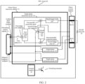
- FIG. 2 is a schematic diagram of a structure of a PFC circuit according to an embodiment of this application.
- the PFC circuit 20 may include an alternating current module 21, a power factor correction module 22, a direct current module 23, and a control module 24.
- the power factor correction module 22 may include a three-phase correction circuit connected in parallel, namely, a single-phase correction circuit 221, a single-phase correction circuit 222, and a single-phase correction circuit 223.
- Each single-phase correction circuit in the foregoing three-phase correction circuit includes at least one inductor and four bridge arms.
- the single-phase correction circuit 221 may specifically include a first inductor L1, a first bridge arm 224, a second bridge arm 225, a third bridge arm 226, and a fourth bridge arm 227.
- One single-phase input/output terminal (for ease of differentiation, an A-phase input/output terminal is used as a replacement for description below) in three single-phase input/output terminals of the alternating current module 21 is connected to one end of the first inductor L1.
- the other end of the first inductor L1 is connected to a bridge arm midpoint of the first bridge arm 224 (for ease of differentiation, a first bridge arm midpoint is used as a replacement for description below).
- the bridge arm midpoint in this embodiment of this application is mainly a symmetry point of the bridge arm.
- the bridge arm includes two switching transistors connected in series
- a connection point between the two switching transistors connected in series is the bridge arm midpoint of the bridge arm.
- the bridge arm includes four switching transistors connected in series
- a connection point between two switching transistors, located on an inner side, in the four switching transistors connected in series is the bridge arm midpoint of the bridge arm.
- the first bridge arm 224 and the second bridge arm 225 are connected in parallel.
- a parallel connection point (which is replaced with a first parallel connection point below) between the first bridge arm 224 and the second bridge arm 225 is connected to one end of the third bridge arm 226, and another parallel connection point (which is replaced with a second parallel connection point below) between the first bridge arm 224 and the second bridge arm 225 is connected to one end of the fourth bridge arm 227.
- the parallel connection point in this embodiment of this application mainly means a connection that enables two bridge arms to be connected in parallel.
- a first end of a bridge arm 1 is connected to a first end of a bridge arm 2, and a second end of the bridge arm 1 is also connected to a second end of the bridge arm 2, so that the bridge arm 1 and the bridge arm 2 are connected in parallel.
- the connected first end and the connected second end between the bridge arm 1 and the bridge arm 2 are two parallel connection points.
- the other end of the third bridge arm 226 is connected to a positive bus (namely, BUS+) of the direct current module 23, and the other end of the fourth bridge arm 227 is connected to a negative bus (namely, BUS-) of the direct current module 23.
- a midpoint or an imaginary midpoint of the alternating current module 21 is connected to the second bridge arm midpoint and the direct current module 23.
- the control module 24 is further separately connected to third ends of switching transistors included in the first bridge arm 224, the second bridge arm 225, the third bridge arm 226, and the fourth bridge arm 227.
- the midpoint (which also referred to as a neutral point) of the alternating current module 21 is a point in a winding of a transformer or a generator corresponding to the alternating current module 21, and absolute values of voltages between this point and input/output terminals of each phase of the alternating current module 21 are equal.
- the imaginary midpoint (which also referred to as a virtual neutral point) of the alternating current module 21 is a common connection point at which the input/output terminals of each phase of the alternating current module 21 are connected together through a corresponding capacitor, and absolute values of voltages between the common connection point and the input/output terminals of each phase of the alternating current module 21 are equal.
- the first inductor L1, the first bridge arm 224, the second bridge arm 225, the third bridge arm 226, and the fourth bridge arm 227 in the single-phase correction circuit 221 form a boost rectifier circuit.
- the first bridge arm 224 is a low-frequency rectification function area
- the second bridge arm 225 is a high-frequency rectification function area
- the third bridge arm 226 and the fourth bridge arm 227 are used as freewheeling transistors.
- the single-phase correction circuit 221 may perform voltage boosting and rectification on a single-phase alternating current (which is assumed to be an A-phase alternating current herein) of a third voltage value V3 flowing from the first inductor L1, and output a direct current of a first voltage value V1 to the direct current module 23.
- a voltage of the positive bus of the direct current module 23 is +(V1/2), and a voltage of the negative bus is -(V1/2), that is, a voltage drop value between the positive bus and the negative bus is V1.
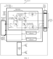
- FIG. 3 is a schematic diagram of another structure of the PFC circuit according to an embodiment of this application.
- the first bridge arm 224 may specifically include a first switching transistor S 1 and a second switching transistor S2 connected in series
- the second bridge arm 225 may specifically include a third switching transistor S3 and a fourth switching transistor S4 connected in series
- the third bridge arm may specifically include a fifth switching transistor S5, and the fourth switching transistor may specifically include a sixth switching transistor S6.
- the first bridge arm midpoint of the first bridge arm 224 is a connection point between a first end of the first switching transistor S 1 and a second end of the second switching transistor S2, and the first parallel connection point is a connection point between a second end of the first switching transistor S1 and a first end of the third switching transistor S3.
- the second parallel connection point between the first bridge arm 224 and the second bridge arm 225 is a connection point between the second end of the second switching transistor S2 and a first end of the fourth switching transistor S4.
- the second bridge arm midpoint of the second bridge arm 225 is a connection point between a second end of the third switching transistor S3 and a second end of the fourth switching transistor S4.
- a first end of the fifth switching transistor S5 is connected to the first parallel connection point, a second end of the fifth switching transistor S5 is connected to the positive bus BUS+, a first end of the sixth switching transistor S6 is connected to the second parallel connection point, and a second end of the sixth switching transistor S6 is connected to the negative bus BUS-.
- Third ends of the first switching transistor S1, the second switching transistor S2, the third switching transistor S3, the fourth switching transistor S4, the fifth switching transistor S5, and the sixth switching transistor S6 are separately connected to the control module 24.
- the second bridge arm midpoint formed by the second end of the third switching transistor S3 and the second end of the fourth switching transistor S4 is connected to the midpoint or the imaginary midpoint provided by the alternating current module 21.
- the control module 24 may control turn-on or turn-off of each switching transistor by using a third end of each switching transistor. Therefore, the third end of each switching transistor may also be understood as a control end of each switching transistor.
- the direct current module 23 may further include a first capacitor C1 and a second capacitor C2 connected in series.
- a first end of the first capacitor C1 and a first end of the second capacitor C2 are simultaneously connected to the midpoint or the imaginary midpoint provided by the alternating current module 21.
- a second end of the first capacitor C1 is connected to the positive bus BUS+.
- a second end of the second capacitor C2 is connected to the negative bus BUS-.
- the first end of the first capacitor C1 and the second capacitor C2 are used as energy storage devices in the direct current module 23.
- voltages at both ends of the first capacitor C1 and the second capacitor are steady at V1/2, so that a steady voltage drop of V1 exists between the positive bus BUS+ and the negative bus BUS-.
- the alternating current module 21 may specifically include a first alternating current source 2101, a second alternating current source 2102, and a third alternating current source 2103.
- a first end of the first alternating current source 2101, a first end of the second alternating current source 2102, and a first end of the third alternating current source 2103 are connected, and are used as the midpoint.
- a second end of the first alternating current source 2101 is connected to the first inductor L1 as the A-phase input/output terminal.
- a second end of the second alternating current source 2102, as another phase input/output terminal (which is assumed to be a B-phase input/output terminal herein) of the alternating current module 21, is connected to an inductor (for ease of differentiation, a second inductor L2 is used as a replacement for description below) in the single-phase correction circuit 222.
- a second end of the third alternating current source 2103, as another phase input/output terminal (it is assumed to be a C-phase input/output terminal herein) of the alternating current module 21, is connected to an inductor (for ease of differentiation, a third inductor L2 is used as a replacement for description below) in the single-phase correction circuit 223.
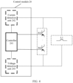
- FIG. 4 is a schematic diagram of a structure of a control module according to an embodiment of this application.
- the control module 24 may specifically include a controller 241, a current detection unit 242, and/or a voltage detection unit 243.
- the controller 241 is connected to control ends of switching transistors (namely, the switching transistors in the first bridge arm 224, the second bridge arm 225, the third bridge arm 226, and the fourth bridge arm 227) included in each single-phase correction circuit, and the control module 24 may control, by using the controller 241, turn-on or turn-off of the switching transistors included in each single-phase correction circuit.
- the controller 241 is further separately connected to the current detection unit 242 and the voltage detection unit 243.
- the current detection unit 242 is further connected to one end of the first inductor in each single-phase correction circuit.
- the current detection unit 242 is configured to detect a current flowing through the first inductor connected to the current detection unit 242, and provide a corresponding current detection result to the controller 241.
- the voltage detection unit 243 is further separately connected to two ports other than the control end of any switching transistor on which voltage detection needs to be performed in each single-phase circuit.
- the voltage detection unit 243 is configured to detect a voltage between the two ports other than the control end of the any switching transistor, and provide a corresponding voltage detection result to the controller 241.
- the controller 241 may be configured to control, based on the current detection result and/or the voltage detection result, turn-on or turn-off of the switching transistors included in the single-phase correction circuits.
- the following uses the single-phase correction circuit 221 as an example. It is assumed that the first inductor L1 needs to perform current detection, and the third switching transistor S3 needs to perform voltage detection.
- gates of the first switching transistor S1, the second switching transistor S2, the third switching transistor S3, the fourth switching transistor S4, the fifth switching transistor S5, and the sixth switching transistor S6 are separately connected to the controller 241.
- One end of the current detection unit 242 is connected to one end of the first inductor L1, and the other end is connected to the controller 241.
- One end of the voltage detection unit 243 is connected to the controller 241, and the other two ends are respectively connected to the drain and the source of the third switching transistor S3.
- the current detection unit 242 may detect a current flowing through the first inductor L1, and provide a detection result to the controller 241.
- the voltage detection unit 243 may detect a voltage value between the source and the drain of the third switching transistor S3, and provide the voltage value to the controller 241.
- the foregoing describes a connection relationship between the current detection unit 242 and the voltage detection unit 243 and a corresponding function by using only an inductor or a switching transistor in the single-phase correction circuit 221 as an example.
- the current detection unit 242 may alternatively be connected to inductors in the single-phase correction circuit 222 and the single-phase correction circuit 223, and implement a corresponding current detection function.
- the voltage detection unit 243 may alternatively be connected to switching transistors in the single-phase correction circuit 222 and the single-phase correction circuit 223, and implement a corresponding voltage detection function. It should be understood herein that different application manners of the current detection unit 242 and the voltage detection unit 243 in the PFC circuit provided in this application may be directly deduced from the examples provided above. Details are not described in this application again.
- control module 24 may not include the current detection unit 242 or the voltage detection unit 243. In other words, whether the control module 24 includes the current detection unit 242 or the voltage detection unit 243 may be set based on an actual application requirement. This is not specifically limited in this application.
- the switching transistor in the PFC circuit provided in this application may be specifically an insulated gate device, for example, an insulated gate bipolar transistor (insulated gate bipolar transistor, IGBT) or a metal-oxide semiconductor field-effect transistor (metal-oxide-semiconductor field-effect transistor, MOSFET).
- IGBT insulated gate bipolar transistor
- MOSFET metal-oxide semiconductor field-effect transistor
- These switching transistors may alternatively be wide-bandgap semiconductor devices, such as silicon carbide and gallium nitride. This is not specifically limited in this application.
- the controller 241 in the PFC circuit provided in this application may include a discrete component or a logic device, for example, a complex programmable logic device (complex programmable logic device, CPLD), a field-programmable gate array (filed-programmable gate array, FPGA), a single-chip microcomputer, or a digital signal processor (digital signal processor, DSP). This is not specifically limited in this application.
- a complex programmable logic device complex programmable logic device
- FPGA field-programmable gate array
- DSP digital signal processor
- the single-phase correction circuit 222 can convert the input B-phase alternating current into a direct current with the first voltage value V1, and output the direct current to the positive bus and the negative bus of the direct current module 23.
- the single-phase correction circuit 223 can also convert the input C-phase alternating current into a direct current with the first voltage value V1, and output the direct current to the positive bus and the negative bus of the direct current module 23.
- structures of the single-phase correction circuit 222 and the single-phase correction circuit 223 are the same as the structure of the single-phase correction circuit 221, and connection relationships between components included in the single-phase correction circuit 222 and the single-phase correction circuit 223 are also the same as those of the single-phase correction circuit 221.
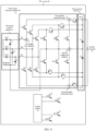
- FIG. 5 is a schematic diagram of another structure of the PFC circuit according to an embodiment of this application.
- FIG. 5 is a schematic diagram of a complete structure of the PFC circuit according to an embodiment of this application.
- the single-phase correction circuit 222 may alternatively include one inductor and four bridge arms (it is assumed herein that a fifth bridge arm, a sixth bridge arm, a seventh bridge arm, and an eighth bridge arm are included), and the inductor may be a second inductor L2.
- the fifth bridge arm may include a seventh switching transistor S7 and an eighth switching transistor S8 connected in series
- the sixth bridge arm may include a ninth switching transistor S9 and a tenth switching transistor S10 connected in series
- the seventh bridge arm may include an eleventh switching transistor S11
- the eighth bridge arm may include a twelfth switching transistor S12.
- a first end of the seventh switching transistor S7 is connected to a first end of the eighth switching transistor S8, a second end of the seventh switching transistor S7 is connected to a first end of the eleventh switching transistor S11, and a second end of the eleventh switching transistor S11 is connected to the positive bus BUS+ of the direct current module 23.
- a second end of the eighth switching transistor S8 is connected to a first end of the twelfth switching transistor S12, and a second end of the twelfth switching transistor S 12 is connected to the negative bus BUS- of the direct current module 23.
- a first end of the ninth switching transistor S9 is connected to a first end of the tenth switching transistor S10, a second end of the ninth switching transistor S9 is connected to the first end of the eleventh switching transistor S11, and a second end of the tenth switching transistor S10 is connected to the first end of the twelfth switching transistor S12.
- Third ends of the seventh switching transistor S7, the eighth switching transistor S8, the ninth switching transistor S9, the tenth switching transistor S10, the eleventh switching transistor S11, and the twelfth switching transistor S12 are separately connected to the control module 24.
- the second ends of the ninth switching transistor S9 and the tenth switching transistor S10 are also simultaneously connected to the midpoint provided by the alternating current module 21.
- the single-phase correction circuit 223 may alternatively include one inductor and four bridge arms (it is assumed herein that a ninth bridge arm, a tenth bridge arm, an eleventh bridge arm, and a twelfth bridge arm are included).
- the inductor may be a third inductor L3.
- the ninth bridge arm may include a thirteenth switching transistor S13 and a fourteenth switching transistor S14 connected in series
- the tenth bridge arm may include a fifteenth switching transistor S15 and a sixteenth switching transistor S16 connected in series
- the eleventh bridge arm may include a seventeenth switching transistor S17
- the twelfth bridge arm may include an eighteenth switching transistor S18.
- a first end of the thirteenth switching transistor S13 is connected to a first end of the fourteenth switching transistor S14, a second end of the thirteenth switching transistor S13 is connected to a first end of the seventeenth switching transistor S17, and a second end of the seventeenth switching transistor S17 is connected to the positive bus BUS+ of the direct current module 23.
- a second end of the fourteenth switching transistor S14 is connected to a first end of the eighteenth switching transistor S18, and a second end of the eighteenth switching transistor S18 is connected to the negative bus BUS- of the direct current module 23.
- a first end of the fifteenth switching transistor S15 is connected to a first end of the sixteenth switching transistor S16, a second end of the fifteenth switching transistor S15 is connected to the first end of the seventeenth switching transistor S17, and a second end of the sixteenth switching transistor S16 is connected to the first end of the eighteenth switching transistor S18.
- Third ends of the thirteenth switching transistor S13, the fourteenth switching transistor S14, the fifteenth switching transistor S15, the sixteenth switching transistor S16, the seventeenth switching transistor S17, and the eighteenth switching transistor S18 are separately connected to the control module 24.
- the second ends of the fifteenth switching transistor S15 and the sixteenth switching transistor S16 are also simultaneously connected to the midpoint provided by the alternating current module 21.
- FIG. 5 shows the structure of the PFC circuit in a scenario in which the alternating current module 21 provides the midpoint.
- the alternating current module 21 may alternatively provide an imaginary midpoint.
- FIG. 6 is a schematic diagram of another structure of the PFC circuit according to an embodiment of this application.
- FIG. 6 is a schematic diagram of another complete structure of the PFC circuit according to an embodiment of this application in a scenario in which the alternating current module 21 provides the imaginary midpoint.
- the alternating current module 21 may further include a third capacitor C3, a fourth capacitor C4, and a fifth capacitor C5.
- a first end of the third capacitor C3 is separately connected to one end of the first alternating current source 2101 and one end of the first inductor L1
- a first end of the fourth capacitor C4 is separately connected to one end of the second alternating current source 2102 and one end of the second inductor L2
- a first end of the fifth capacitor C5 is separately connected to one end of the third alternating current source 2103 and one end of the third inductor L3, and a second end of the third capacitor C3, a second end of the fourth capacitor C4, and a second end of the fifth capacitor C5 are simultaneously connected to the power factor correction module 22 and the direct current module 23 as the imaginary midpoint of the alternating current module 21.
- FIG. 7 is a schematic flowchart of a PFC circuit control method according to an embodiment of this application.
- the PFC circuit control method may be specifically performed by the control module 24 described above. It should be noted herein that, because the single-phase correction circuit 221, the single-phase correction circuit 222, and the single-phase correction circuit 223 in the power factor correction module 22 all use the PFC circuit control method provided in this embodiment of this application, to avoid repetition, the following uses the single-phase correction circuit 221 as an example to describe in detail a specific implementation process of the PFC circuit control method provided in this application. In addition, switching frequencies of the third switching transistor S3, the fourth switching transistor S4, the fifth switching transistor S5, and the sixth switching transistor S6 are far greater than a frequency of the A-phase alternating current.
- the method includes the following steps.
- a control module determines whether an alternating current on a single-phase input/output terminal is in a positive half cycle or a negative half cycle.
- control module 24 in the PFC circuit 20 may first determine whether the alternating current (namely, the A-phase alternating current) flowing through the single-phase input/output terminal (namely, the foregoing A-phase input/output terminal) is in the positive half cycle or the negative half cycle. If the control module 24 determines that the A-phase alternating current is in the positive half cycle, the control module 24 may determine to perform the following step S702.
- each cycle of the alternating current may be divided into a positive half cycle and a negative half cycle based on a current direction.
- a cycle Tn of the A-phase alternating current is used as an example.
- the current direction is a time period in which the current flows out of the single-phase input/output terminal of the alternating current module 21 and flows in the midpoint or the imaginary midpoint of the alternating current module 21, that is, a positive half cycle corresponding to the cycle Tn. It may also be understood that, in this time period, the A-phase alternating current is in a positive half cycle.
- the current direction is a time period in which the current flows out of the midpoint or the imaginary midpoint of the alternating current module 21 and flows in the single-phase input/output terminal of the alternating current module 21, that is, a negative half cycle corresponding to the cycle Tn. It may also be understood that, in this time period, the A-phase alternating current is in a negative half cycle.
- the control module turns on or turns off switching transistors on the first bridge arm and the second bridge arm if determining that the alternating current is in the positive half cycle, to boost a first voltage at the first parallel connection point.
- the control module 24 when the control module 24 determines that the A-phase alternating current is in a positive half cycle (which is assumed to be a positive half cycle T1 herein), the control module may turn on or turn off the switching transistors on the first bridge arm 224 and the second bridge arm 225, to boost the first voltage at the first parallel connection point based on a freewheeling function of the first inductor L1.
- a positive half cycle T1 is used as an example for description in the following part.
- this embodiment of this application provides a plurality of optional implementations of boosting the first voltage. The following separately describes the plurality of implementations in detail.
- the control module 24 may keep the first switching transistor S1 in a turn-on state in the positive half cycle T1. In other words, when the control module 24 determines that the A-phase alternating current is at a start moment of the positive half cycle T1, that is, the first switching transistor S1 is turned on, the turn-on state lasts until an end moment of the positive half cycle T1 expires. In addition, the control module 24 may further turn off the second switching transistor S2, the fourth switching transistor S4, and the sixth switching transistor S6.
- the control module 24 may turn on the third switching transistor S3.
- the first preset moment t1 is included in the positive half cycle T1.
- the control module 24 may alternatively turn on the third switching transistor S3 when determining that a voltage at the first parallel connection point is equal to a voltage at the second bridge arm midpoint. It may be understood herein that a voltage drop between the first parallel connection point and the second bridge arm midpoint is essentially a voltage (which is assumed to be VS3 herein) between the source and the drain of the third switching transistor S3. For ease of description, the voltage between the source and the drain of the switching transistor is collectively referred to as a terminal voltage of the switching transistor in the following part. Therefore, in specific implementation, the control module 24 may detect the terminal voltage VS3 of the third switching transistor S3 in real time by using the voltage detection unit 243.
- the control module 24 may determine that the voltage at the first parallel connection point is equal to the voltage at the third parallel connection point.
- the third switching transistor S3 is turned on when voltages at two ends of the third switching transistor S3 are the same. That is, zero voltage turn-on of the third switching transistor S3 is implemented, and a switching loss of the PFC circuit can be reduced.
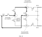
- FIG. 8 is a schematic diagram of a circuit status according to an embodiment of this application.
- a current loop passes through the first inductor L1, the first switching transistor S1, the third switching transistor S3, and an alternating current source 2101, and a current direction is a preset first current direction.
- the first inductor L1 is in a charging state, and a current (for ease of differentiation, the first current is used as a replacement for description below) flowing through the first inductor L1 gradually increases in the first current direction.
- the control module 24 may preferentially determine, based on whether the first preset moment expires, whether to turn on the third switching transistor S3. After the entire PFC circuit enters the steady state, the control module 24 may preferentially determine, based on whether the voltage at the first parallel connection point is equal to the voltage at the second bridge arm midpoint (that is, whether the terminal voltage VS3 is zero), whether to turn on the third switching transistor S3.
- the control module 24 may turn off the third switching transistor S3.
- a current direction of the second preset current is the first current direction
- a magnitude of the second preset current may be a preset second current value (which is assumed to be i2 herein).
- the control module 24 may determine that a direction of the first current is the first current direction and a current value of the first current is the second current value i2, the third switching transistor S3 may be turned off. It should be understood herein that, in real-time working, a factor such as a detection error is considered.
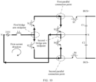
- FIG. 9 is a schematic diagram of another circuit status according to an embodiment of this application.
- the control module 24 turns off the third switching transistor S3
- the first inductor L1 starts to release energy stored in the first inductor L1.
- the current direction of the first inductor L1 is still the first current direction.
- electric energy released by the first inductor L1 charges a parasitic capacitor (which is assumed to be C6 herein) of the third switching transistor S3 and a parasitic capacitor (which is assumed to be C7 herein) of the fifth switching transistor S5 through the first parallel connection point.
- the first voltage at the first parallel connection point gradually increases. In this way, the first voltage is boosted.
- the control module 24 may keep the first switching transistor S1 and the fourth switching transistor S4 in a turn-on state in the positive half cycle T1.
- the control module 24 may further turn off the sixth switching transistor S6.
- the control module 24 may turn on the second switching transistor S2 and the third switching transistor S3 when determining that the first preset moment t1 expires.
- the first preset moment t1 for a description of the first preset moment t1, refer to the foregoing description. Details are not described herein again.
- control module 24 may alternatively turn on the second switching transistor S2 and the third switching transistor S3 when determining that the voltage at the first parallel connection point is equal to the voltage at the second bridge arm midpoint.
- control module 24 determines that the voltage at the first parallel connection point is equal to the voltage at the second bridge arm midpoint. Details are not described herein again.
- a voltage drop at two ends of the third switching transistor S3 and the second switching transistor S2 is zero. In this case, the second switching transistor S2 and the third switching transistor S3 are turned on.
- the control module 24 may preferentially determine, based on whether the first preset moment t1 expires, whether to turn on the second switching transistor S2 and the third switching transistor S3. After the entire PFC circuit enters the steady state, the control module 24 may preferentially determine, based on whether the voltage at the first parallel connection point is equal to the voltage at the second bridge arm midpoint, whether to turn on the second switching transistor S2 and the third switching transistor S3.
- FIG. 10 is a schematic diagram of another circuit status according to an embodiment of this application.
- the second switching transistor S2 and the third switching transistor S3 are turned on, there are two current loops (which are assumed to be a first current loop and a second current loop herein), and current directions in the two current loops are both the first current direction.
- the first current loop passes through the first inductor L1, the first switching transistor S1, the third switching transistor S3, and the alternating current source 2101
- the second current loop passes through the first inductor L1, the second switching transistor S2, the fourth switching transistor S4, and the alternating current source 2101.
- the first inductor L1 is in a charging state, and the first current flowing through the first inductor L1 gradually increases in the first current direction.
- the control module 24 may turn off the second switching transistor S2 and the third switching transistor S3. Refer to FIG. 9 . After the control module 24 turns off the second switching transistor S2 and the third switching transistor S3, the first inductor L1 starts to release energy stored in the first inductor L1. However, due to the freewheeling characteristic of the inductor, the current direction of the first inductor L1 is still the first current direction.
- control module 24 may keep the first switching transistor S1 and the fourth switching transistor S4 in a turn-on state in the positive half cycle T1. In addition, the control module 24 may further turn off the sixth switching transistor S6.
- the control module 24 may turn on the third switching transistor S3 when determining that the first preset moment t1 expires.
- first preset moment t1 for a description of the first preset moment t1, refer to the foregoing description. Details are not described herein again.
- control module 24 may alternatively turn on the third switching transistor S3 when determining that the voltage at the first parallel connection point is equal to the voltage at the second bridge arm midpoint.
- the control module 24 determines that the voltage at the first parallel connection point is equal to the voltage at the second bridge arm midpoint. Details are not described herein again.
- a voltage drop at two ends of the third switching transistor S3 is zero.
- the third switching transistor S3 is turned on. That is, zero voltage turn-on of the third switching transistor S3 is implemented, and a switching loss of the PFC circuit can be reduced.
- control module 24 may preferentially determine, based on whether the first preset moment t1 expires, whether to turn on the third switching transistor S3. After the entire PFC circuit enters the steady state, the control module 24 may preferentially determine, based on whether the voltage at the first parallel connection point is equal to the voltage at the second bridge arm midpoint, whether to turn on the third switching transistor S3.
- control module 24 turns on the second switching transistor S2 when determining that first preset duration (which is assumed to be dt1 herein) expires.
- a start moment of the first preset duration d11 is a turn-on moment of the third switching transistor.
- the second switching transistor S2 is turned on when a voltage drop at two ends is zero. That is, zero voltage turn-on of the second switching transistor S2 is implemented, and a switching loss of the PFC circuit can be reduced.
- control module 24 may turn off the second switching transistor S2 when determining that second preset duration (which is assumed to be dt2 herein) expires.
- a start moment of the second preset duration dt2 is a turn-on moment of the second switching transistor S2. It can be understood herein that, because the first switching transistor S1 and the third switching transistor S3 are still in a turn-on state when the second switching transistor S2 is turned off, the second switching transistor S2 is turned off when a zero voltage exists. This further implements zero voltage turn-off of the second switching transistor S2, and further reduces a switching loss of the PFC circuit.
- the control module 24 may turn off the third switching transistor S3.
- the control module 24 may turn off the third switching transistor S3.
- the first inductor L1 starts to release energy stored in the first inductor L1.
- the current direction of the first inductor L1 is still the first current direction.
- electric energy released by the first inductor L1 charges a parasitic capacitor C6 of the third switching transistor S3, a parasitic capacitor C7 of the fifth switching transistor S5, and a parasitic capacitor C8 of the second switching transistor.
- the first voltage at the first parallel connection point gradually increases. In this way, the first voltage is boosted.
- the control module turns on a switching transistor on the third bridge arm when determining that a boosted first voltage is equal to a voltage of the positive bus of the direct current module.
- the control module 24 may detect whether the boosted first voltage is equal to the voltage of the positive bus BUS+ of the direct current module 23.
- the control module 24 may turn on the fifth switching transistor S5 included in the third bridge arm 226 when determining that the boosted first voltage is equal to the voltage of the positive bus BUS+.
- a voltage drop at two ends of the fifth switching transistor S5 is zero.
- the fifth switching transistor S5 is turned on. That is, zero voltage turn-on of the fifth switching transistor S5 is implemented, and a switching loss of the PFC circuit can be further reduced.
- FIG. 11 is a schematic diagram of another circuit status according to an embodiment of this application. As shown in FIG. 11 , after the fifth switching transistor S5 is turned on, the first inductor L1 continues to release energy, and the current loop passes through the first inductor L1, the first switching transistor S1, the fifth switching transistor S5, the first capacitor C1, and the alternating current source 2101, to form a boost loop, and the first capacitor C1 is charged.
- FIG. 12 is another schematic flowchart of a PFC circuit control method according to an embodiment of this application. As shown in FIG. 12 , the control method may further include the following steps.
- the control module turns off the fifth switching transistor if determining that a current of the first inductor is equal to a first preset current.
- control module 24 may determine whether the first current is equal to the first preset current. The control module 24 may turn off the fifth switching transistor S5 if determining that the first current is equal to the first preset current.
- control module 24 may detect a magnitude and a direction of the first current by using the current detection unit 242.
- the control module 24 may turn off the fifth switching transistor S5.
- the first preset current when the third voltage value V3 described above is less than half of the first voltage value V1, the first preset current may be a zero current.
- the magnitude of the first preset current may be a preset first current value (which is assumed to be i1 herein), and the direction of the first preset current may be a second current direction opposite to the first current direction.
- control module 24 determines to be still in the positive half cycle T1
- the control module 24 repeatedly performs actions of the step S702, the step S703, and the step S704 until the positive half cycle T1 ends.
- the parasitic capacitor C6 and the parasitic capacitor C7 resonate with the first inductor L1 because the parasitic capacitor C6 and the parasitic capacitor C7 exist.
- the direction of the first current of the first inductor L1 changes from the original first current direction to the opposite second current direction. Due to a current function in the opposite direction, the voltage at the first parallel connection point gradually decreases.
- the control module 24 may turn on the third switching transistor S3 again when detecting that the terminal voltage VS3 of the third switching transistor S3 is zero again, and then the control module 24 may perform subsequent actions corresponding to implementation 1 and actions of the step S703 and the step S704. Such processing is repeatedly performed until the positive half cycle T1 ends. It should be noted herein that, in the scenario of implementation 1, the first switching transistor S1 is turned on, and the second switching transistor S2, the fourth switching transistor S4, and the sixth switching transistor S6 are turned off. Therefore, in subsequent repeated actions, only the third switching transistor S3 and the fifth switching transistor S5 need to be controlled to be turned on or turned off, and states of other switching transistors should keep unchanged.
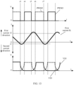
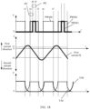
- FIG. 13 is a schematic diagram of a waveform according to an embodiment of this application.
- FIG. 13 shows waveforms of control signals (a PWM wave is used as an example herein, and it is assumed that a control signal of the third switching transistor is PWM3, and a control signal of the fifth switching transistor is PWM5) of the third switching transistor S3 and the fifth switching transistor S5, waveforms of terminal voltages (namely, VS3 and VS5) of the third switching transistor S3 and the fifth switching transistor S5, and waveforms of the first current of the first inductor L1 after the PCF circuit enters a steady state.
- FIG. 13 shows waveforms of control signals (a PWM wave is used as an example herein, and it is assumed that a control signal of the third switching transistor is PWM3, and a control signal of the fifth switching transistor is PWM5) of the third switching transistor S3 and the fifth switching transistor S5, waveforms of terminal voltages (namely, VS3 and VS5) of the third switching transistor S3 and the fifth switching transistor S5, and
- the control module 24 may control the PWM5 to be at a low level when determining that the direction of the first current is the second current direction and the magnitude is i2 (that is, at a moment t3 shown in the figure). In this case, both the fifth switching transistor S5 and the third switching transistor S3 are in a turn-off state.
- the control module 24 controls the PWM3 to be at a high level, and turns on the third switching transistor S3 when determining that the terminal voltage VS3 of the third switching transistor S3 is zero (that is, at a moment t4 shown in the figure). This implements zero level turn-on of the third switching transistor. Then, the control module 24 may control the PWM3 to be at a low level when determining that the direction of the first current is the first current direction, and the magnitude of the first current is the first current value i1 (that is, at a moment t5 shown in the figure). In this case, the third switching transistor S3 is turned off.
- a terminal voltage VS5 of the fifth switching transistor S5 gradually decreases until the terminal voltage VS5 is equal to 0 (that is, at a moment t6 in the figure), the PWM5 may be controlled to be at a high level, and the fifth switching transistor S5 is turned on. This implements zero level turn-on of the fifth switching transistor S5.
- the first current IL gradually decreases until the control module 24 determines again that the direction of the first current is the second current direction, and the magnitude is i1 (that is, at a moment t7 shown in the figure), the PWM5 may be controlled to be at a low level, and the fifth switching transistor S5 is turned off.
- the entire circuit returns again to a state in which both the fifth switching transistor S5 and the third switching transistor S3 are turned off, and the control module 24 may continue to repeat control on turn-on or turn-off of the third switching transistor S3 and the fifth switching transistor S5.
- the control module 24 turns on the second switching transistor S2 and the third switching transistor S3 when detecting that voltages at two ends of the third switching transistor S3 are equal, and then the control module 24 may perform subsequent actions corresponding to implementation 2 and actions of the step S703 and the step S704. Such processing is repeatedly performed until the positive half cycle T1 ends. It should be noted herein that, in the scenario of implementation 2, the first switching transistor S1 is turned on, and the fourth switching transistor S4 and the sixth switching transistor S6 are turned off. Therefore, in subsequent repeated actions, only the second switching transistor S2, the third switching transistor S3, and the fifth switching transistor S5 need to be controlled to be turned on or turned off, and states of other switching transistors should keep unchanged.
- FIG. 13 a waveform of a switching transistor signal (which is assumed to be PWM2 herein) of the second switching transistor S2 is completely the same as that of the control signal PWM3 of the third switching transistor S3.
- a change waveform of the terminal voltage of the second switching transistor S2 is also the same as that of the terminal voltage of the third switching transistor S3. Therefore, FIG. 13 is still used as an example for description herein. As shown in FIG.
- the control module 24 may control the PWM5 to be at a low level when determining that the direction of the first current is the second current direction and the magnitude is i1 (that is, at a moment t3 shown in the figure).
- the fifth switching transistor S5, the second switching transistor S2, and the third switching transistor S3 are all in a turn-off state.
- the control module 24 controls the PWM3 and the PWM2 to be at a high level, and turns on the second switching transistor S2 and the third switching transistor S3 when determining that the terminal voltage VS3 of the third switching transistor S3 is zero (that is, at the moment t4 shown in the figure).
- control module 24 may control the PWM3 and the PWM2 to be at a low level when determining that the direction of the first current is the first current direction, and the magnitude of the first current is the first current value i1 (that is, at the moment t5 shown in the figure). In this case, the second switching transistor S2 and the third switching transistor S3 are turned off.
- the terminal voltage VS5 of the fifth switching transistor S5 gradually decreases until the terminal voltage VS5 is equal to 0 (that is, at the moment t6 in the figure), the PWM5 may be controlled to be at a high level, and the fifth switching transistor S5 is turned on. This implements zero level turn-on of the fifth switching transistor S5.
- the third switching transistor S5 is turned on, the first current IL gradually decreases until the control module 24 determines again that the direction of the first current is the second current direction, and the magnitude is i1 (that is, at the moment t7 shown in the figure), the PWM5 may be controlled to be at a low level, and the fifth switching transistor S5 is turned off.
- the entire circuit returns again to a state in which the fifth switching transistor S5, the second switching transistor S2, and the third switching transistor S3 are all turned off, and the control module 24 may continue to repeat control on turn-on or turn-off of the second switching transistor S2, the third switching transistor S3, and the fifth switching transistor S5.
- the control module 24 first turns on the third switching transistor S3 when detecting that voltages at two ends of the third switching transistor S3 are equal, and then turns on the second switching transistor S2 when another first preset duration dt1 expires. Then, the second switching transistor S2 is turned off when another second preset duration dt2 expires. Then, the third switching transistor S3 is turned off when it is determined that the first current is equal to the first preset current again. Then, the control module 24 may continue to perform actions of the step S703 and the step S704. Such processing is repeatedly performed until the positive half cycle T1 ends.
- the first switching transistor S1 and the fourth switching transistor S4 are turned on, and the sixth switching transistor S6 is turned off. Therefore, in subsequent repeated actions, only the second switching transistor S2, the third switching transistor S3, and the fifth switching transistor S5 need to be controlled to be turned on or turned off, and states of other switching transistors should keep unchanged.
- FIG. 14 is a schematic diagram of another waveform according to an embodiment of this application.
- FIG. 14 shows waveforms of control signals (which are respectively PWM2, PWM3, and PWM5) of the second switching transistor S2, the third switching transistor S3, and the fifth switching transistor S5, waveforms of terminal voltages (namely, VS3 and VS5) of the third switching transistor S3 and the fifth switching transistor S5, and waveforms of the first current of the first inductor L1 after the PCF circuit enters a steady state.
- control signals which are respectively PWM2, PWM3, and PWM5
- terminal voltages namely, VS3 and VS5
- the control module 24 may control the PWM5 to be at a low level when determining that the direction of the first current is the second current direction and the magnitude is i1 (that is, at a moment t3 shown in the figure).
- the fifth switching transistor S5, the second switching transistor S2, and the third switching transistor S3 are all in a turn-off state.
- the control module 24 controls the PWM3 to be at a high level, and turns on the third switching transistor S3 when determining that the terminal voltage VS3 of the third switching transistor S3 is zero (that is, at a moment t4 shown in the figure). This implements zero level turn-on of the third switching transistor S3.
- control module 24 may control the PWM2 to be at a high level and turn on the second switching transistor S2 when determining that first preset duration dt1 expires (that is, when a moment t8 shown in the figure expires, a time difference between the moment t8 and the moment t4 is the first preset duration dt1). In this case, zero voltage turn-on of the second switching transistor S2 is implemented.
- the control module 24 may control the PWM2 to be at a low level, and turn on the second switching transistor S2 when determining that second preset duration dt2 expires (that is, when a moment t9 shown in the figure expires, a time difference between the moment t9 and the moment t8 is the second preset duration dt2). In this case, zero voltage turn-off of the second switching transistor S2 is implemented. Then, the control module 24 may control the PWM3 to be at a low level when determining that the direction of the first current is the first current direction, and the magnitude of the first current is the first current value i1 (that is, at a moment t5 shown in the figure). In this case, the third switching transistor S3 is turned off.
- the terminal voltage VS5 of the fifth switching transistor S5 gradually decreases until the terminal voltage VS5 is equal to 0 (that is, at a moment t6 in the figure), the PWM5 may be controlled to be at a high level, and the fifth switching transistor S5 is turned on. This implements zero level turn-on of the fifth switching transistor S5.
- the third switching transistor S5 is turned on, the first current IL gradually decreases until the control module 24 determines again that the direction of the first current is the second current direction, and the magnitude is i1 (that is, at a moment t7 shown in the figure), the PWM5 may be controlled to be at a low level, and the fifth switching transistor S5 is turned off.
- the entire circuit returns again to a state in which the fifth switching transistor S5, the second switching transistor S2, and the third switching transistor S3 are all turned off, and the control module 24 may continue to repeat control on turn-on or turn-off of the second switching transistor S2, the third switching transistor S3, and the fifth switching transistor S5.
- FIG. 15 is another schematic flowchart of a PFC circuit control method according to an embodiment of this application. As shown in FIG. 15 , the control method further includes the following steps.
- the control module turns on or turns off the switching transistors on the first bridge arm and the second bridge arm if determining that the alternating current is in the negative half cycle, to buck a second voltage at the second parallel connection point.
- the control module 24 when the control module 24 determines that the A-phase alternating current is in a negative half cycle (which is assumed to be a negative half cycle T1 herein), the control module may turn on or turn off the switching transistors on the first bridge arm 224 and the second bridge arm 225, to buck the second voltage at the second parallel connection point by using the freewheeling function of the first inductor L1. It should be noted that, because a plurality of negative half cycles exist in the A-phase alternating current, and control logic in each negative half cycle is the same, a negative half cycle T1 is used as an example for description in the following part.
- this application provides a plurality of optional implementations in which the control module 24 turns on or turns off the switching transistors on the first bridge arm 224 and the second bridge arm 225 to buck the second voltage by using the first inductor L1.
- the control module 24 turns on or turns off the switching transistors on the first bridge arm 224 and the second bridge arm 225 to buck the second voltage by using the first inductor L1.
- the control module 24 may keep the second switching transistor S2 in a turn-on state in the negative half cycle T2. In other words, when the control module 24 determines that the A-phase alternating current is in the negative half cycle T2, that is, the second switching transistor S2 is turned on, the turn-on state lasts until the negative half cycle T2 ends. In addition, the control module 24 may further turn off the first switching transistor S1, the third switching transistor S3, and the fifth switching transistor S5.
- the control module 24 may turn on the fourth switching transistor S4.
- the second preset moment t2 is included in the negative half cycle T2.
- the control module 24 may turn on the fourth switching transistor S4 when determining that a voltage (namely, the second voltage) at the second parallel connection point is equal to a voltage at the second bridge arm midpoint. It may be understood herein that a voltage drop between the second parallel connection point and the second bridge arm midpoint is essentially a voltage (which is assumed to be VS4 herein) between two ends of the fourth switching transistor S4. Therefore, when a terminal voltage S4 of the fourth switching transistor S4 is zero, the fourth switching transistor S4 is turned on. That is, zero voltage turn-on of the fourth switching transistor S4 is implemented, and a switching loss of the PFC circuit is also reduced.
- the current loop passes through the fourth switching transistor S4, the second switching transistor S2, the first inductor L1, and the alternating current source 2101, and the current direction is the second current direction opposite to the first current direction.
- the first inductor L1 is in a charging state, and a current (for ease of differentiation, a third current is used as a replacement for description below) flowing through the first inductor L1 gradually increases in the second current direction.
- the control module 24 may preferentially determine, based on whether the second preset moment t2 expires, whether to turn on the fourth switching transistor S4. After the entire PFC circuit enters the steady state, the control module 24 may preferentially determine, based on whether the voltage at the second parallel connection point is equal to the voltage at the second bridge arm midpoint, whether to turn on the fourth switching transistor S4.
- control module 24 may turn off the fourth switching transistor S4 when determining that the current of the first inductor (namely, the first current) is equal to a fourth preset current.
- a direction of the fourth preset current is the second direction
- a magnitude of the fourth preset current is a preset fourth current value (which is assumed to be i4 herein).
- the control module 24 may keep the second switching transistor S2 and the third switching transistor S3 in a turn-on state in the negative half cycle T2. In other words, when the control module 24 determines that the A-phase alternating current is in the negative half cycle T2, that is, the second switching transistor S2 and the third switching transistor S3 are turned on, the turn-on state lasts until an end moment of the negative half cycle T2 expires. In addition, the control module 24 may further turn off the fifth switching transistor S5.
- control module 24 may turn on the first switching transistor S1 and the fourth switching transistor S4 when determining that the second preset moment t2 expires.
- the control module 24 may turn on the first switching transistor S1 and the fourth switching transistor S4 when determining that the second preset moment t2 expires.
- control module 24 may alternatively turn on the first switching transistor S1 and the fourth switching transistor S4 when determining that the voltage at the second parallel connection point is equal to the voltage at the second bridge arm midpoint.
- the control module 24 may alternatively turn on the first switching transistor S1 and the fourth switching transistor S4 when determining that the voltage at the second parallel connection point is equal to the voltage at the second bridge arm midpoint.
- a voltage drop at two ends of the first switching transistor S1 and the fourth switching transistor S4 is zero.
- the first switching transistor S1 and the fourth switching transistor S4 are turned on. That is, zero voltage turn-on of the first switching transistor S1 and the fourth switching transistor S4 is implemented, and a switching loss of the PFC circuit can be further reduced.
- an equivalent resistance value between the first bridge arm midpoint and the second bridge arm midpoint becomes smaller. This can further reduce a turn-on loss of the PFC circuit.
- control module 24 may preferentially determine, based on whether the second preset moment t2 expires, whether to turn on the first switching transistor S1 and the fourth switching transistor S4. After the entire PFC circuit enters the steady state, the control module 24 may preferentially determine, based on whether the voltage at the second parallel connection point is equal to the voltage at the second bridge arm midpoint, whether to turn on the first switching transistor S1 and the fourth switching transistor S4.
- the first inductor L1 After the first switching transistor S1 and the fourth switching transistor S4 are turned on, the first inductor L1 is in a charging state, and the third current flowing through the first inductor L1 gradually increases in the second current direction.
- the control module 24 may turn off the first switching transistor S1 and the fourth switching transistor S4. After the control module 24 turns off the first switching transistor S1 and the fourth switching transistor S4, the first inductor L1 starts to release energy stored in the first inductor L1. However, due to the freewheeling characteristic of the inductor, the current direction of the first inductor L1 is still the second current direction. In a process in which the first inductor L1 releases energy, electric energy stored in the parasitic capacitor C9 and the parasitic capacitor C10 is extracted by using the second parallel connection point. Therefore, as the energy of the first inductor L1 is released, the second voltage at the second parallel connection point gradually decreases. In this way, the second voltage is bucked.
- control module 24 may keep the second switching transistor S2 and the third switching transistor S3 in a turn-on state in the negative half cycle T2. In addition, the control module 24 may further turn off the fifth switching transistor S5.
- control module 24 may turn on the fourth switching transistor S4 when determining that the second preset moment t2 expires.
- the control module 24 may turn on the fourth switching transistor S4 when determining that the second preset moment t2 expires.
- control module 24 may alternatively turn on the fourth switching transistor S4 when determining that the voltage at the second parallel connection point is equal to the voltage at the second bridge arm midpoint.
- the fourth switching transistor S4 is turned on. That is, zero voltage turn-on of the fourth switching transistor S4 is implemented, and a switching loss of the PFC circuit can be reduced.
- control module 24 may preferentially determine, based on whether the second preset moment t2 expires, whether to turn on the fourth switching transistor S4. After the entire PFC circuit enters the steady state, the control module 24 may preferentially determine, based on whether the voltage at the second parallel connection point is equal to the voltage at the second bridge arm midpoint, whether to turn on the fourth switching transistor S4.
- control module 24 turns on the first switching transistor S1 when determining that third preset duration (which is assumed to be dt3 herein) expires.
- a start moment of the third preset duration dt3 is a turn-on moment of the fourth switching transistor S4.
- the first switching transistor S1 is turned on when a voltage drop at two ends is zero. That is, zero voltage turn-on of the first switching transistor S 1 is implemented, and a switching loss of the PFC circuit can be reduced.
- the first inductor L1 After the first switching transistor S1 is also turned on, the first inductor L1 is in a charging state, and the third current flowing through the first inductor L1 gradually increases in the second current direction.
- control module 24 may turn off the first switching transistor S1 when determining that fourth preset duration (which is assumed to be dt4 herein) expires.
- a start moment of the fourth preset duration dt4 is a turn-on moment of the first switching transistor S1. It may be understood herein that, because the second switching transistor S2, the third switching transistor S3, and the fourth switching transistor S4 are still in a turn-on state when the first switching transistor S1 is turned off, the first switching transistor S1 is turned off when a zero voltage exists. This further implements zero voltage turn-off of the first switching transistor S1, and may further reduce a switching loss of the PFC circuit.
- the control module 24 may turn off the fourth switching transistor S4.
- the first inductor L1 starts to release energy stored in the first inductor L1.
- the current direction of the first inductor L1 is still the second current direction.
- the first inductor L1 releases energy
- electric energy stored in the parasitic capacitor C9 and the parasitic capacitor C10 is extracted by using the second parallel connection point. Therefore, as the energy of the first inductor L1 is released, the second voltage at the second parallel connection point gradually decreases. In this way, the second voltage is bucked.
- the control module turns on the sixth switching transistor when determining that a bucked second voltage is equal to a voltage of the negative bus of the direct current module.
- the control module 24 may detect whether the bucked second voltage is equal to the voltage of the negative bus BUS- of the direct current module 23.
- the control module 24 may turn on the sixth switching transistor S6 when determining that the bucked second voltage is equal to the voltage of the negative bus BUS-.
- a voltage drop at two ends of the sixth switching transistor S6 is zero.
- the sixth switching transistor S6 is turned on. That is, zero voltage switching of the sixth switching transistor S6 is implemented, and a switching loss of the PFC circuit can be further reduced.
- the sixth switching transistor S6 After the sixth switching transistor S6 is turned on, the first inductor L1 continues to release energy, and the current loop passes through the alternating current source 2101, the second capacitor C2, the sixth switching transistor S6, the second switching transistor S2, and the first inductor L1, to form a boost loop, and the second capacitor C2 is charged.
- FIG. 16 is another schematic flowchart of a PFC circuit control method according to an embodiment of this application. As shown in FIG. 16 , the control method may further include the following steps.
- the control module turns off the sixth switching transistor if determining that the current of the first inductor is equal to a third preset current.
- control module 24 may detect a current flowing through the first inductor L1, and turn off the sixth switching transistor S6 when determining that the first current is equal to the third preset current.
- control module 24 may detect a magnitude and a direction of the first current by using the current detection unit 243.
- the control module 24 may turn off the sixth switching transistor S6.
- the third preset current is a zero current.
- the magnitude of the third preset current is the preset third current value (which is assumed to be i3 herein), and the direction of the third preset current is the first current direction.
- control module 24 determines to be still in the negative half cycle T2 if the control module 24 determines to be still in the negative half cycle T2, the control module 24 repeatedly performs actions of the step S705, the step S706, and the step S707 until the negative half cycle T2 ends.
- the parasitic capacitor C8 and the parasitic capacitor C8 resonate with the first inductor L1 because the parasitic capacitor C8 and the parasitic capacitor C9 exist.
- a current in the first current direction (which is assumed to be a fourth current herein) exists in the first inductor L1. Due to a function of the fourth current, the voltage at the second parallel connection point gradually increases.
- the control module 24 turns on the fourth switching transistor S4 when detecting that voltages at two ends of the fourth switching transistor S4 are equal (that is, the voltage at the second parallel connection point is equal to the voltage at the second bridge arm midpoint), and then the control module 24 may perform subsequent actions corresponding to implementation 4 and actions of the step S706 and the step S707. Such processing is repeatedly performed until the negative half cycle T2 ends. It should be noted herein that, in the scenario of implementation 4, the second switching transistor S2 is turned on, and the first switching transistor S 1, the third switching transistor S3, and the fifth switching transistor S5 are turned off. Therefore, in subsequent repeated actions, only the fourth switching transistor S4 and the sixth switching transistor S6 need to be controlled to be turned on or turned off, and states of other switching transistors should keep unchanged.
- FIG. 17 is a schematic diagram of another waveform according to an embodiment of this application.
- FIG. 18 shows waveforms of control signals (a PWM wave is used as an example herein, and it is assumed that a control signal of the fourth switching transistor S4 is PWM4, and a control signal of the sixth switching transistor S6 is PWM6) of the fourth switching transistor S4 and the sixth switching transistor S6, waveforms of terminal voltages (namely, VS4 and VS6) of the fourth switching transistor S4 and the sixth switching transistor S6, and waveforms of the first current of the first inductor L1 after the PCF circuit enters a steady state.
- FIG. 18 shows waveforms of control signals (a PWM wave is used as an example herein, and it is assumed that a control signal of the fourth switching transistor S4 is PWM4, and a control signal of the sixth switching transistor S6 is PWM6) of the fourth switching transistor S4 and the sixth switching transistor S6, waveforms of terminal voltages (namely, VS4 and VS6) of the fourth switching transistor S4 and
- the control module 24 may control the PWM6 to be at a low level, and turn off the sixth switching transistor S6 when determining that the magnitude of the first current is i3 and the direction is the first direction (that is, at a moment t3 shown in the figure). In this case, both the fourth switching transistor S4 and the sixth switching transistor S6 are in a turn-off state.
- the control module 24 may control the PWM4 to be at a high level when determining that the terminal voltage VS4 of the fourth switching transistor S4 is zero (that is, at a moment t4 shown in the figure). In this case, the fourth switching transistor S4 is turned on. That is, zero level turn-on of the fourth switching transistor S4 is implemented. Then, as the first current gradually increases in the second current direction, the control module 24 may control the PWM4 to be at a low level when determining that the direction of the first current is the second current direction and the magnitude is the fourth current value i4 (that is, at a moment t5 shown in the figure). In this case, the fourth switching transistor S4 is turned off.
- the control module 24 may control the PWM6 to be at a high level, and turn on the sixth switching transistor S6.
- the current in the first inductor L1 gradually decreases until the control module 24 determines that the direction of the first current of the first inductor L1 is the first current direction and the magnitude is the third current value i3 (that is, at a moment t7 shown in the figure).
- control module 24 may control the PWM6 to be at a low level, and the circuit returns to a state in which both the fourth switching transistor S4 and the sixth switching transistor S6 are turned off. Then, the control module 24 may continue to repeat control on turn-on or turn-off of the fourth switching transistor S4 and the sixth switching transistor S6.
- the control module 24 turns on the first switching transistor S1 and the fourth switching transistor S4 when detecting that voltages at two ends of the fourth switching transistor S4 are equal, and then the control module 24 may perform subsequent actions corresponding to implementation 5 and actions of the step S706 and the step S707. Such processing is repeatedly performed until the negative half cycle T2 ends. It should be noted herein that, in the scenario of implementation 5, the second switching transistor S2 and the third switching transistor S3 are turned on, and the fifth switching transistor S5 is turned off. Therefore, in subsequent repeated actions, only the first switching transistor S1, the fourth switching transistor S4, and the sixth switching transistor S6 need to be controlled to be turned on or turned off, and states of other switching transistors should keep unchanged.
- FIG. 17 a waveform of a switching transistor signal (which is assumed to be PWM1 herein) of the first switching transistor S1 is completely the same as that of the control signal PWM4 of the fourth switching transistor S4.
- a change waveform of the terminal voltage of the first switching transistor S1 is also the same as that of the terminal voltage of the fourth switching transistor S4. Therefore, FIG. 17 is still used as an example for description herein.
- control module 24 may control the PWM6 to be at a low level, and turn off the sixth switching transistor S6 when determining that the magnitude of the first current is i3 and the direction is the first direction (that is, at a moment t3 shown in the figure).
- the first switching transistor S1, the fourth switching transistor S4, and the sixth switching transistor S6 are all in a turn-off state.
- the control module 24 may control the PW1 and the PWM4 to be at a high level when determining that the terminal voltage VS4 of the fourth switching transistor S4 is zero (that is, at a moment t4 shown in the figure). In this case, the first switching transistor S1 and the fourth switching transistor S4 are turned on.
- the control module 24 may control the PW1 and the PWM4 to be at a low level when determining that the direction of the first current is the second current direction and the magnitude is the fourth current value i4 (that is, at a moment t5 shown in the figure). In this case, the first switching transistor S1 and the fourth switching transistor S4 are turned off. After the first switching transistor S1 and the fourth switching transistor S4 are turned off, the first level is pulled down until the control module 24 determines that the terminal voltage VS6 of the sixth switching transistor S6 is equal to zero (that is, at a moment t6 shown in the figure).
- the control module 24 may control the PWM6 to be at a high level, and turn on the sixth switching transistor S6. After the sixth switching transistor S6 is turned on, the current in the first inductor L1 gradually decreases until the control module 24 determines that the direction of the first current of the first inductor L1 is the first current direction and the magnitude is the third current value i3 (that is, at a moment t7 shown in the figure). In this case, the control module 24 may control the PWM6 to be at a low level, and the circuit returns to a state in which the first switching transistor S1, the fourth switching transistor S4, and the sixth switching transistor S6 are all turned off. Then, the control module 24 may continue to repeat control on turn-on or turn-off of the first switching transistor S 1, the fourth switching transistor S4, and the sixth switching transistor S6.
- the control module 24 first turns on the fourth switching transistor S4 when detecting that voltages at two ends of the fourth switching transistor S4 are equal, and then turns on the first switching transistor S1 when another third preset duration dt3 expires. Then, the first switching transistor S1 is turned off when another fourth preset duration dt4 expires. Then, the fourth switching transistor S4 is turned off when it is determined that the first current is equal to the fourth preset current. Then, the control module 24 may continue to perform actions of the step S706 and the step S707. Such processing is repeatedly performed until the negative half cycle T2 ends.
- the second switching transistor S2 and the third switching transistor S3 are turned on, and the fifth switching transistor S5 is turned off. Therefore, in subsequent repeated actions, only the first switching transistor S 1, the fourth switching transistor S4, and the sixth switching transistor S6 need to be controlled to be turned on or turned off, and states of other switching transistors should keep unchanged.
- FIG. 18 is a schematic diagram of another waveform according to an embodiment of this application.
- FIG. 18 shows waveforms of control signals (which are respectively PWM1, PWM4, and PWM6) of the first switching transistor S1, the fourth switching transistor S4, and the sixth switching transistor S6, waveforms of terminal voltages (namely, VS4 and VS6) of the fourth switching transistor S4 and the sixth switching transistor S6, and waveforms of the first current of the first inductor L1 after the PCF circuit enters a steady state.
- FIG. 18 is also described by using an example in which the third voltage value V3 is equal to or greater than half of the first voltage value V1, that is, the third preset current is the first current direction, and the magnitude is i3.
- control module 24 may control the PWM6 to be at a low level, and turn off the sixth switching transistor S6 when determining that the magnitude of the first current is i3 and the direction is the first direction (that is, at a moment t3 shown in the figure).
- the first switching transistor S1, the fourth switching transistor S4, and the sixth switching transistor S6 are all in a turn-off state.
- the control module 24 may control the PWM4 to be at a high level when determining that the terminal voltage VS4 of the fourth switching transistor S4 is zero (that is, at a moment t4 shown in the figure).
- the fourth switching transistor S4 is turned on. That is, zero level turn-on of the fourth switching transistor S4 is implemented.
- the control module may control the PWM1 to be at a high level, and turn on the first switching transistor S1.
- VS4 is zero, and therefore, zero level turn-on of the first switching transistor S1 is implemented.
- the control module may control the PWM1 to be at a low level, and turn off the first switching transistor S1.
- VS4 is still zero, and therefore, zero level turn-off of the first switching transistor S1 is implemented.
- the control module 24 may control the PWM4 to be at a low level when determining that the direction of the first current is the second current direction and the magnitude is the fourth current value i4 (that is, at a moment t5 shown in the figure).
- the fourth switching transistor S4 is turned off. After the fourth switching transistor S4 is turned off, the first level is pulled down until the control module 24 determines that the terminal voltage VS6 of the sixth switching transistor S6 is equal to zero (that is, at a moment t6 shown in the figure). In this case, the control module 24 may control the PWM6 to be at a high level, and turn on the sixth switching transistor S6. After the sixth switching transistor S6 is turned on, the current in the first inductor L1 gradually decreases until the control module 24 determines that the direction of the first current of the first inductor L1 is the first current direction and the magnitude is the third current value i3 (that is, at a moment t7 shown in the figure).
- control module 24 may control the PWM6 to be at a low level, and the circuit returns to a state in which the first switching transistor S1, the fourth switching transistor S4, and the sixth switching transistor S6 are all turned off. Then, the control module 24 may continue to repeat control on turn-on or turn-off of the first switching transistor S1, the fourth switching transistor S4, and the sixth switching transistor S6.
- each preset parameter (for example, the first preset moment t1, the first preset duration dt1, and the first preset current) in this embodiment of this application may be specifically an empirical value obtained by performing a plurality of tests on the PFC circuit provided in this application. Specific values of these preset parameters are not limited in this application.
- the PFC circuit 20 may further perform inversion and voltage bucking on an input direct current with a second voltage value Vout, to output an alternating current whose effective value is a first voltage value Vin.
- Specific control logic is the same as that described above, and is not described herein again.
- the control module 24 in the PFC circuit can implement zero voltage switching of one or more switching transistors in any single-phase correction circuit included in the control module 24. In this way, a switching loss and a turn-on loss of the PFC circuit can be significantly reduced, and performance of the PFC circuit can be effectively improved.
Landscapes
- Engineering & Computer Science (AREA)
- Power Engineering (AREA)
- Rectifiers (AREA)
Applications Claiming Priority (1)
| Application Number | Priority Date | Filing Date | Title |
|---|---|---|---|
| PCT/CN2021/121486 WO2023050103A1 (fr) | 2021-09-28 | 2021-09-28 | Procédé de commande de circuit de correction de facteur de puissance (pfc) et circuit de pfc |
Publications (2)
| Publication Number | Publication Date |
|---|---|
| EP4380025A1 true EP4380025A1 (fr) | 2024-06-05 |
| EP4380025A4 EP4380025A4 (fr) | 2024-09-25 |
Family
ID=85781002
Family Applications (1)
| Application Number | Title | Priority Date | Filing Date |
|---|---|---|---|
| EP21958696.3A Withdrawn EP4380025A4 (fr) | 2021-09-28 | 2021-09-28 | Procédé de commande de circuit de correction de facteur de puissance (pfc) et circuit de pfc |
Country Status (4)
| Country | Link |
|---|---|
| US (1) | US20240243655A1 (fr) |
| EP (1) | EP4380025A4 (fr) |
| CN (1) | CN117652085A (fr) |
| WO (1) | WO2023050103A1 (fr) |
Family Cites Families (6)
| Publication number | Priority date | Publication date | Assignee | Title |
|---|---|---|---|---|
| CN102624213B (zh) * | 2012-03-29 | 2014-12-03 | 台达电子工业股份有限公司 | 一种功率因数校正电路 |
| CN102843025B (zh) * | 2012-08-06 | 2015-01-07 | 台达电子工业股份有限公司 | 用于pfc电路的控制电路、控制方法及电源系统 |
| US9362844B2 (en) * | 2013-06-14 | 2016-06-07 | Hamilton Sundstrand Corporation | Method of deriving switch current signals in a rectifier |
| CN104638692B (zh) * | 2013-11-08 | 2017-08-25 | 艾默生网络能源有限公司 | 一种不间断电源的蓄电池组挂接电路以及不间断电源 |
| US9647533B2 (en) * | 2013-11-08 | 2017-05-09 | One More Time Llc | PFC circuits with very low THD |
| CN112440768B (zh) * | 2019-09-05 | 2022-07-15 | 比亚迪股份有限公司 | 充电控制方法、充电控制模块及其存储介质 |
-
2021
- 2021-09-28 CN CN202180099272.XA patent/CN117652085A/zh active Pending
- 2021-09-28 WO PCT/CN2021/121486 patent/WO2023050103A1/fr not_active Ceased
- 2021-09-28 EP EP21958696.3A patent/EP4380025A4/fr not_active Withdrawn
-
2024
- 2024-03-27 US US18/617,923 patent/US20240243655A1/en not_active Abandoned
Also Published As
| Publication number | Publication date |
|---|---|
| US20240243655A1 (en) | 2024-07-18 |
| EP4380025A4 (fr) | 2024-09-25 |
| CN117652085A (zh) | 2024-03-05 |
| WO2023050103A1 (fr) | 2023-04-06 |
Similar Documents
| Publication | Publication Date | Title |
|---|---|---|
| CN102005928B (zh) | 光伏高频隔离升压软开关dc/dc变换器及其控制方法 | |
| US9685881B2 (en) | AC-DC rectifier system | |
| CN105141135B (zh) | 一种级联电源系统中多路并联全桥llc变换器的控制方法 | |
| EP4047805B1 (fr) | Dispositif de commande et système de commande pour convertisseur cc/cc | |
| EP3255771A1 (fr) | Convertisseur bidirectionnel courant continu-courant continu | |
| CN114123203A (zh) | 一种交流电网电压不平衡时直流母线电压纹波抑制策略 | |
| CN106612072A (zh) | 基于buck拓扑的开关电源控制电路及太阳能控制器 | |
| JP2017530677A (ja) | Dc−dc直列共振コンバータを有したバッテリ充電器を制御する方法 | |
| EP4391341A1 (fr) | Convertisseur de courant continu multiniveau, procédé de commande de tension pour condensateur volant, et appareil de commande | |
| CN106992535B (zh) | 一种电能路由器高压直流母线电容的恒电流预充电方法 | |
| US8830701B2 (en) | DC-DC converter | |
| EP4622082A1 (fr) | Circuit d'alimentation électrique et appareil approprié pour une sortie à large plage, système et procédé de commande | |
| Fatyga et al. | Comparison of main control strategies for DC/DC stage of bidirectional vehicle charger | |
| CN116349125A (zh) | 电压转换电路的控制方法、装置及电子设备 | |
| Zhang et al. | Three-level PWM rectifier based high efficiency batteries charger for EV | |
| Zhang et al. | A high efficiency two-stage ZVS AC/DC converter with all SiC MOSFET | |
| Vuchev et al. | Analysis of continuous current mode of an LLC resonant DC-DC converter at ZVS | |
| CN104134991A (zh) | 一种面向直流微电网的三端口直流母线稳压模块 | |
| US20240243655A1 (en) | Power factor correction pfc circuit control method and pfc circuit | |
| CN119765433A (zh) | 变流器架构及控制方法、电池包、及储能系统 | |
| Jiang et al. | A single-stage 6.78 MHz transmitter with the improved light load efficiency for wireless power transfer applications | |
| Akssas et al. | Bidirectional On-Board charger based on the efficient topology Vienna Rectifier | |
| Halder | An improved performance of the soft switching buck converter | |
| Xu et al. | A bidirectional symmetrical C4LC-DCX resonant converter with power limitation capability | |
| CN113890198A (zh) | 一种基于直流降压和输出电流控制的电感线圈充放电源 |
Legal Events
| Date | Code | Title | Description |
|---|---|---|---|
| STAA | Information on the status of an ep patent application or granted ep patent |
Free format text: STATUS: THE INTERNATIONAL PUBLICATION HAS BEEN MADE |
|
| PUAI | Public reference made under article 153(3) epc to a published international application that has entered the european phase |
Free format text: ORIGINAL CODE: 0009012 |
|
| STAA | Information on the status of an ep patent application or granted ep patent |
Free format text: STATUS: REQUEST FOR EXAMINATION WAS MADE |
|
| 17P | Request for examination filed |
Effective date: 20240301 |
|
| AK | Designated contracting states |
Kind code of ref document: A1 Designated state(s): AL AT BE BG CH CY CZ DE DK EE ES FI FR GB GR HR HU IE IS IT LI LT LU LV MC MK MT NL NO PL PT RO RS SE SI SK SM TR |
|
| A4 | Supplementary search report drawn up and despatched |
Effective date: 20240822 |
|
| RIC1 | Information provided on ipc code assigned before grant |
Ipc: H02M 7/487 20070101ALN20240817BHEP Ipc: H02M 1/00 20060101ALI20240817BHEP Ipc: H02M 1/42 20070101AFI20240817BHEP |
|
| DAV | Request for validation of the european patent (deleted) | ||
| DAX | Request for extension of the european patent (deleted) | ||
| STAA | Information on the status of an ep patent application or granted ep patent |
Free format text: STATUS: THE APPLICATION HAS BEEN WITHDRAWN |
|
| 18W | Application withdrawn |
Effective date: 20250310 |