EP4380137A1 - Elektronische vorrichtung mit flexibler leiterplatte - Google Patents
Elektronische vorrichtung mit flexibler leiterplatte Download PDFInfo
- Publication number
- EP4380137A1 EP4380137A1 EP22878839.4A EP22878839A EP4380137A1 EP 4380137 A1 EP4380137 A1 EP 4380137A1 EP 22878839 A EP22878839 A EP 22878839A EP 4380137 A1 EP4380137 A1 EP 4380137A1
- Authority
- EP
- European Patent Office
- Prior art keywords
- section
- housing
- electronic device
- circuit board
- printed circuit
- Prior art date
- Legal status (The legal status is an assumption and is not a legal conclusion. Google has not performed a legal analysis and makes no representation as to the accuracy of the status listed.)
- Pending
Links
Images


Classifications
-
- H—ELECTRICITY
- H05—ELECTRIC TECHNIQUES NOT OTHERWISE PROVIDED FOR
- H05K—PRINTED CIRCUITS; CASINGS OR CONSTRUCTIONAL DETAILS OF ELECTRIC APPARATUS; MANUFACTURE OF ASSEMBLAGES OF ELECTRICAL COMPONENTS
- H05K1/00—Printed circuits
- H05K1/02—Details
- H05K1/14—Structural association of two or more printed circuits
- H05K1/148—Arrangements of two or more hingeably connected rigid printed circuit boards, i.e. connected by flexible means
-
- G—PHYSICS
- G06—COMPUTING OR CALCULATING; COUNTING
- G06F—ELECTRIC DIGITAL DATA PROCESSING
- G06F1/00—Details not covered by groups G06F3/00 - G06F13/00 and G06F21/00
- G06F1/16—Constructional details or arrangements
- G06F1/1613—Constructional details or arrangements for portable computers
- G06F1/1615—Constructional details or arrangements for portable computers with several enclosures having relative motions, each enclosure supporting at least one I/O or computing function
- G06F1/1616—Constructional details or arrangements for portable computers with several enclosures having relative motions, each enclosure supporting at least one I/O or computing function with folding flat displays, e.g. laptop computers or notebooks having a clamshell configuration, with body parts pivoting to an open position around an axis parallel to the plane they define in closed position
-
- G—PHYSICS
- G06—COMPUTING OR CALCULATING; COUNTING
- G06F—ELECTRIC DIGITAL DATA PROCESSING
- G06F1/00—Details not covered by groups G06F3/00 - G06F13/00 and G06F21/00
- G06F1/16—Constructional details or arrangements
- G06F1/1613—Constructional details or arrangements for portable computers
- G06F1/1633—Constructional details or arrangements of portable computers not specific to the type of enclosures covered by groups G06F1/1615 - G06F1/1626
- G06F1/1637—Details related to the display arrangement, including those related to the mounting of the display in the housing
- G06F1/1652—Details related to the display arrangement, including those related to the mounting of the display in the housing the display being flexible, e.g. mimicking a sheet of paper, or rollable
-
- G—PHYSICS
- G06—COMPUTING OR CALCULATING; COUNTING
- G06F—ELECTRIC DIGITAL DATA PROCESSING
- G06F1/00—Details not covered by groups G06F3/00 - G06F13/00 and G06F21/00
- G06F1/16—Constructional details or arrangements
- G06F1/1613—Constructional details or arrangements for portable computers
- G06F1/1633—Constructional details or arrangements of portable computers not specific to the type of enclosures covered by groups G06F1/1615 - G06F1/1626
- G06F1/1675—Miscellaneous details related to the relative movement between the different enclosures or enclosure parts
- G06F1/1681—Details related solely to hinges
-
- G—PHYSICS
- G06—COMPUTING OR CALCULATING; COUNTING
- G06F—ELECTRIC DIGITAL DATA PROCESSING
- G06F1/00—Details not covered by groups G06F3/00 - G06F13/00 and G06F21/00
- G06F1/16—Constructional details or arrangements
- G06F1/1613—Constructional details or arrangements for portable computers
- G06F1/1633—Constructional details or arrangements of portable computers not specific to the type of enclosures covered by groups G06F1/1615 - G06F1/1626
- G06F1/1675—Miscellaneous details related to the relative movement between the different enclosures or enclosure parts
- G06F1/1683—Miscellaneous details related to the relative movement between the different enclosures or enclosure parts for the transmission of signal or power between the different housings, e.g. details of wired or wireless communication, passage of cabling
-
- H—ELECTRICITY
- H04—ELECTRIC COMMUNICATION TECHNIQUE
- H04M—TELEPHONIC COMMUNICATION
- H04M1/00—Substation equipment, e.g. for use by subscribers
- H04M1/02—Constructional features of telephone sets
- H04M1/0202—Portable telephone sets, e.g. cordless phones, mobile phones or bar type handsets
- H04M1/0206—Portable telephones comprising a plurality of mechanically joined movable body parts, e.g. hinged housings
- H04M1/0208—Portable telephones comprising a plurality of mechanically joined movable body parts, e.g. hinged housings characterized by the relative motions of the body parts
- H04M1/0214—Foldable telephones, i.e. with body parts pivoting to an open position around an axis parallel to the plane they define in closed position
- H04M1/0216—Foldable in one direction, i.e. using a one degree of freedom hinge
- H04M1/022—The hinge comprising two parallel pivoting axes
-
- H—ELECTRICITY
- H05—ELECTRIC TECHNIQUES NOT OTHERWISE PROVIDED FOR
- H05K—PRINTED CIRCUITS; CASINGS OR CONSTRUCTIONAL DETAILS OF ELECTRIC APPARATUS; MANUFACTURE OF ASSEMBLAGES OF ELECTRICAL COMPONENTS
- H05K1/00—Printed circuits
- H05K1/02—Details
- H05K1/0277—Bendability or stretchability details
- H05K1/028—Bending or folding regions of flexible printed circuits
- H05K1/0281—Reinforcement details thereof
-
- H—ELECTRICITY
- H05—ELECTRIC TECHNIQUES NOT OTHERWISE PROVIDED FOR
- H05K—PRINTED CIRCUITS; CASINGS OR CONSTRUCTIONAL DETAILS OF ELECTRIC APPARATUS; MANUFACTURE OF ASSEMBLAGES OF ELECTRICAL COMPONENTS
- H05K5/00—Casings, cabinets or drawers for electric apparatus
- H05K5/02—Details
- H05K5/0217—Mechanical details of casings
- H05K5/0226—Hinges
-
- H—ELECTRICITY
- H04—ELECTRIC COMMUNICATION TECHNIQUE
- H04M—TELEPHONIC COMMUNICATION
- H04M1/00—Substation equipment, e.g. for use by subscribers
- H04M1/02—Constructional features of telephone sets
- H04M1/0202—Portable telephone sets, e.g. cordless phones, mobile phones or bar type handsets
- H04M1/026—Details of the structure or mounting of specific components
- H04M1/0266—Details of the structure or mounting of specific components for a display module assembly
- H04M1/0268—Details of the structure or mounting of specific components for a display module assembly including a flexible display panel
-
- H—ELECTRICITY
- H04—ELECTRIC COMMUNICATION TECHNIQUE
- H04M—TELEPHONIC COMMUNICATION
- H04M1/00—Substation equipment, e.g. for use by subscribers
- H04M1/02—Constructional features of telephone sets
- H04M1/0202—Portable telephone sets, e.g. cordless phones, mobile phones or bar type handsets
- H04M1/026—Details of the structure or mounting of specific components
- H04M1/0274—Details of the structure or mounting of specific components for an electrical connector module
-
- H—ELECTRICITY
- H05—ELECTRIC TECHNIQUES NOT OTHERWISE PROVIDED FOR
- H05K—PRINTED CIRCUITS; CASINGS OR CONSTRUCTIONAL DETAILS OF ELECTRIC APPARATUS; MANUFACTURE OF ASSEMBLAGES OF ELECTRICAL COMPONENTS
- H05K2201/00—Indexing scheme relating to printed circuits covered by H05K1/00
- H05K2201/10—Details of components or other objects attached to or integrated in a printed circuit board
- H05K2201/10007—Types of components
- H05K2201/10128—Display
Definitions
- Various embodiments disclosed in the disclosure relate to an electronic device including a flexible printed circuit board.
- a mobile electronic device such as a smartphone may provide various functions, such as calling, playing videos, Internet search, etc., based on various kinds of applications.
- a user may wish to use the above-described functions through a larger screen, but portability of an electronic device may be degraded as the size thereof increases.
- a foldable electronic device which enhances portability by utilizing a folding structure may be provided.
- the foldable electronic device may include a hinge structure, and a first housing and a second housing which are connected with each other by the hinge structure to be connected in opposite directions to be rotatable.
- the foldable electronic device may include a printed circuit board which connects electronic components disposed on the housings separated with reference to the hinge structure, respectively.
- the printed circuit board may include a flexible printed circuit board which has some areas bendable when the foldable electronic device is folded or unfolded.
- a height of a hinge housing in which at least part of a flexible printed circuit board is disposed may be reduced.
- a space for accommodating the flexible printed circuit board may be reduced, and a variance in the curvature of a bending area of the flexible printed circuit board may increase.
- a stress generated in the bending area by the bending of the flexible printed circuit board may increase. For example, if some areas of the flexible printed circuit board have a narrow width than their adjacent areas, the narrow area may be relatively easily broken by a force applied from the outside.
- an electronic device may include: a hinge structure which is a folding area and includes a hinge housing; a first housing connected to the hinge structure; a second housing connected with the first housing through the hinge structure to be rotatable with respect to the first housing; and a flexible printed circuit board (FPCB), which has a first end connected to a first printed circuit board (PCB) disposed in the first housing, and a second end connected to a second PCB disposed in the second housing.
- a hinge structure which is a folding area and includes a hinge housing
- a first housing connected to the hinge structure
- a second housing connected with the first housing through the hinge structure to be rotatable with respect to the first housing
- FPCB flexible printed circuit board
- the FPCB may include a first section and a second section, the second section is extended from a first side of the first section, and a variance in a curvature of the second section may be greater than a variance in a curvature of the first section when the first housing and the second housing rotate with respect to the hinge structure.
- an electronic device may include: a hinge structure which is a folding area and includes a hinge housing; a first housing connected to the hinge structure; a second housing connected with the first housing through the hinge structure to be rotatable with respect to the first housing; and an FPCB which has a first end connected to a first PCB disposed in the first housing, and a second end connected to a second PCB disposed in the second housing.
- the FPCB may include: a first section including a curvature when the first housing and the second housing are folded or unfolded through the hinge structure; and a second section which is extended from a first side of the first section, and is disposed to form a linear area at least part of which has a flat surface in the folded state of the first housing and the second housing, and to form a curvature in the unfolded state, and a variance in a curvature of the second section may be greater than a variance in a curvature of the first section when the first housing and the second housing rotate with respect to the hinge structure.
- an electronic device may include: a hinge structure which is a folding area and includes a hinge housing; a first housing connected to the hinge structure; a second housing connected with the first housing through the hinge structure to be rotatable with respect to the first housing; and an FPCB, which has a first end connected to a first PCB disposed in the first housing, and a second end connected to a second PCB disposed in the second housing.
- the FPCB may include a first section, a second section, and a third section, the second section is extended from one side of the first section, and the third section is extended from one side of the second section, and a variance in a curvature of the first section may be greater than a variance in a curvature of at least one of the second section or the third section when the first housing and the second housing rotate with respect to the hinge structure.
- Various embodiments of the disclosure provide an electronic device including a flexible printed circuit board, which may effectively prevent the flexible printed circuit board from being damaged, by reducing a change in a curvature of a bent area of the flexible printed circuit board caused by bending of the flexible printed circuit board.
- various embodiments of the disclosure provide an electronic device which has durability of a flexible printed circuit board enhanced without including an additional stiffener.
- An electronic device may include at least one of, for example, smartphones, tablet personal computers (PCs), mobile phones, video telephones, electronic book readers, desktop PCs, laptop PCs, netbook computers, workstations, servers, personal digital assistant (PDAs), portable multimedia players (PMPs), Motion Picture Experts Group (MPEG-1 or MPEG-2) Audio Layer 3 (MP3) players, mobile medical devices, cameras, or wearable devices.
- PCs tablet personal computers
- PDAs personal digital assistant
- PMPs portable multimedia players
- MPEG-1 or MPEG-2 Motion Picture Experts Group Audio Layer 3
- MP3 Motion Picture Experts Group Audio Layer 3
- the wearable devices may include at least one of accessories (for example, watches, rings, bracelets, ankle bracelets, necklaces, glasses, contact lenses, head-mounted-devices (HMDs), etc.), fabric- or clothing-mounted devices (for example, electronic apparels), body-mounted devices (for example, skin pads, tattoos, etc.), or bio-implantable circuits.
- accessories for example, watches, rings, bracelets, ankle bracelets, necklaces, glasses, contact lenses, head-mounted-devices (HMDs), etc.
- fabric- or clothing-mounted devices for example, electronic apparels
- body-mounted devices for example, skin pads, tattoos, etc.
- bio-implantable circuits for example, watches, rings, bracelets, ankle bracelets, necklaces, glasses, contact lenses, head-mounted-devices (HMDs), etc.
- fabric- or clothing-mounted devices for example, electronic apparels
- body-mounted devices for example, skin pads, tattoos, etc.
- bio-implantable circuits for example, watches, rings,
- the electronic device may be a home appliance.
- the home appliance may include at least one of, for example, televisions (TVs), digital video disk (DVD) players, audios, refrigerators, air conditioners, cleaners, ovens, microwave ovens, washing machines, air cleaners, set-top boxes, home automation control panels, security control panels, TV boxes, game consoles, electronic dictionaries, electronic keys, camcorders, or electronic picture frames.
- TVs televisions
- DVD digital video disk
- the electronic device may include at least one of medical devices (for example, various portable medical measurement devices (for example, a blood glucose monitoring device, a heartbeat measuring device, a blood pressure measuring device, a body temperature measuring device, and the like), a magnetic resonance angiography (MRA), a magnetic resonance imaging (MRI), a computed tomography (CT), scanners, and ultrasonic devices), navigation devices, global navigation satellite systems (GNSS), event data recorders (EDRs), flight data recorders (FDRs), vehicle infotainment devices, electronic equipment for vessels (for example, navigation systems and gyrocompasses), avionics, security devices, head units for vehicles, industrial or home robots, automatic teller's machines (ATMs) of financial institutions, points of sales (POSs) of stores, or Internet of things (for example, light bulbs, various sensors, electricity or gas meters, sprinkler devices, fire alarms, thermostats, street lamps, toasters, exercise equipment, hot water tanks, heaters, boilers, or the like).
- medical devices for
- the electronic device may include at least one of furniture, a part of buildings/structures, electronic boards, electronic signature receiving devices, projectors, or various measuring instruments (for example, water meters, electricity meters, gas meters, or wave meters).
- the electronic device may be one or a combination of two or more devices of the above-mentioned devices.
- the electronic device may be a flexible electronic device.
- the electronic device according to various embodiments of the disclosure is not limited to the above-mentioned devices, and may include new electronic devices according to technology development.
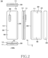
- FIG. 1 is a view illustrating a first state (flat state) 100A of an electronic device according to an embodiment.
- FIG. 2 is a view illustrating a second state (folded state) 100B of the electronic device according to an embodiment.
- the electronic device 100 may include a housing 110, a hinge cover 230 to cover a foldable portion of the housing 110, and a flexible or foldable display 200 (hereinafter, referred to as a "main display" 200) disposed in a space formed by the housing 110.
- a surface on which the main display 200 is disposed is defined as a first surface or a front surface 101 of the electronic device 100.
- the opposite surface of the front surface 101 is defined as a second surface or a rear surface 102 of the electronic device 100.
- a surface surrounding a space between the front surface 101 and the rear surface 102 is defined as a third surface or a side surface 103 of the electronic device 100.
- the housing 110 may include a foldable housing.
- the housing 110 may include a first housing 111, a second housing 112, a first rear surface cover 180, and a second rear surface cover 190.
- the housing 110 of the electronic device 100 is not limited to the shape and coupling illustrated in FIGS. 1 and 2 , and may be implemented by a combination and/or coupling of other shapes or components.
- the first housing 111 and the first rear surface cover 180 may be integrally formed with each other
- the second housing 112 and the second rear surface cover 190 may be integrally formed with each other.
- a state in which the electronic device 100 is unfolded may refer to the flat state 100A or the first state 100A.
- a state in which the first housing 111 and the second housing 112 are unfolded may correspond to the flat state 100A or the first state 100A.
- a state in which the electronic device 100 is folded may refer to the folded state 100B or the second state 100B.
- a state in which the second housing 112 rotates with respect to the first housing 111 and is folded may correspond to the folded state 100B or the second state 100B.
- the first housing 111 and the second housing 112 may have an angle or a distance therebetween that is changed according to whether the electronic device 100 is in a flat state, a folded state, or an intermediate state.
- the first housing 111 and the second housing 112 may be disposed on both sides with reference to a folding axis (hereinafter, a "first axis"), and may have a substantially symmetrical shape with respect to the first axis.
- first axis a folding axis
- the first housing 111 and the second housing 112 may have an asymmetrical shape in some areas.
- the second housing 112 may further include a USB hole 151, differently from the first housing 111.
- the first housing 111 and the second housing 112 may include portions that have a symmetrical shape and portions that have an asymmetrical shape.
- the main display 200 may be symmetrically disposed over the first housing 111 and the second housing 112.
- At least part of the first housing 111 and the second housing 112 may be formed with a metallic material or a nonmetallic material having stiffness of a level selected to support the main display 200.
- the first rear surface cover 180 may be disposed on one side of the first axis on the rear surface of the electronic device.
- the first rear surface cover 180 may have a substantially rectangular periphery, and may have the periphery surrounded by the first housing 111.
- the second rear surface cover 190 may be disposed on the other side of the first axis on the rear surface of the electronic device, and may have the periphery surrounded by the second housing 112.
- first rear surface cover 180 and the second rear surface cover 190 may have a substantially symmetrical shape with reference to the first axis.
- first rear surface cover 180 and the second rear surface cover 190 may not necessarily have the symmetrical shape, and in another embodiment, the electronic device 100 may include the first rear surface cover 180 and the second rear surface cover 190 of various shapes.
- the first rear surface cover 180, the second rear surface cover 190, the first housing 111, and the second housing 112 may form a space to have various components (for example, a printed circuit board or a battery) of the electronic device 100 disposed therein.
- one or more components may be disposed on the rear surface of the electronic device 100 or may be visually exposed.
- at least part of a sub display 220 may be visually exposed through a first rear surface area 181 of the first rear surface cover 180.
- the sub display 220 may be disposed on the entirety of the first rear surface area 231 of the first rear surface cover 180.
- one or more components or a sensor may be visually exposed through a second rear surface area 232 of the second rear surface cover 190.
- the sensor may include a proximity sensor and/or a rear-facing camera 280.
- the main display 200 may be disposed on the space formed by the housing 110.
- the main display 200 may be seated on a recess formed by the housing 110, and may form most of the front surface 101 of the electronic device 100.
- the front surface 101 of the electronic device 100 may include the main display 200, and some areas of the first housing 111 and some areas of the second housing 112 which are adjacent to the main display 200.
- the rear surface 102 of the electronic device 100 may include the first rear surface cover 180, some areas of the first housing 111 that are adjacent to the first rear surface cover 180, the second rear surface cover 190, and some areas of the second housing 112 that are adjacent to the second rear surface cover 190.
- the main display 200 may refer to a display that has at least some areas deformable to a flat surface or a curved surface.
- the main display 200 may include a folding area 203, a first display area 201 disposed on one side (the left of the folding area 203 show in FIG. 1 ) with reference to the folding area 203, and a second display area 202 disposed on the other side (the right of the folding area 203 shown in FIG. 1 ).
- the divided areas of the main display 200 shown in FIG. 1 are examples and the main display 200 may be divided into a plurality of areas (for example, four or more areas or two areas) according to a structure or a function of the main display 200.
- the main display 200 may be divided into areas by the folding area 203 extended in parallel with the y-axis or the first axis (folding axis), but in another embodiment, the main display 200 may be divided into areas with reference to another folding area (for example, a folding area parallel to the x-axis) or another folding axis (for example, a folding axis parallel to the x-axis).
- the first display area 201 and the second display area 202 may have a substantially symmetrical shape with reference to the folding area 203.
- the second display area 202 may include a camera hole 150, differently from the first display area 201, but may have a symmetrical shape with the first display area 201 on the other area.
- the first display area 201 and the second display area 202 may include portions that have a symmetrical shape and portions that have an asymmetrical shape.
- the camera hole 150 may be visually exposed to the outside of the electronic device 100. According to another embodiment, the camera hole 150 may be disposed on a lower portion of the main display 200 not to be visually exposed.
- the first housing 111 and the second housing 112 may form the angle of 180° and may be disposed to face in the same direction.
- a surface of the first display area 201 of the main display 200 and a surface of the second display area 202 may form the angle of 180° with each other, and may face in the same direction (for example, the front surface direction of the electronic device).
- the folding area 203 may form the same plane as the first display area 201 and the second display area 202.
- the first housing 111 and the second housing 112 may be disposed to face each other.
- the surface of the first display area 201 of the main display 200 and the surface of the second display area 202 of the main display 200 may face each other while forming a small angle (for example, between 0° and 10°) with each other.
- At least part of the folding area 203 may have a curved surface having a predetermined curvature.
- the first housing 111 and the second housing 112 may be disposed with a certain angle therebetween.
- the surface of the first display area 201 of the main display 200 and the surface of the second display area 202 of the main display 200 may form an angle that is larger than the angle in the folded state and is smaller than the angle in the flat state.
- At least part of the folding area 203 may have a curved surface having a predetermined curvature, and the curvature in this state may be smaller than in the folded state.
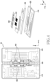
- FIG. 3 is an exploded perspective view of an electronic device according to an embodiment.
- the electronic device 100 may include a display unit 20, a bracket assembly 30, a board unit 300, a first housing 111, a second housing 112, a first rear surface cover 180, and a second rear surface cover 190.
- the display unit 20 may be referred to as a display module or a display assembly.
- the display unit 20 may include a main display 200 and one or more plates or layers (not shown) on which the main display 200 is seated.
- the plate may be disposed between the main display 200 and the bracket assembly 30.
- the main display 200 may be disposed on at least part of one surface (for example, an upper surface in FIG. 3 ) of the plate.
- the plate may be formed in a shape corresponding to the main display 200.
- the bracket assembly 30 may include a bracket 310 including a first bracket 311, a second bracket 312, a hinge structure 305 disposed between the first bracket 311 and the second bracket 312, a hinge housing 330 to cover the hinge structure 305 when it is viewed from the outside, and a wire member 343 (for example, a flexible printed circuit (FPC)) crossing over the first bracket 311 and the second bracket 312.
- a wire member 343 for example, a flexible printed circuit (FPC)
- the hinge housing 330 may be disposed between the first housing 111 and the second housing 112, and may be configured to hide inner components (for example, the hinge structure 305). In an embodiment, the hinge housing 330 may be hidden by a part of the first housing 111 and the second housing 112, or may be exposed to the outside, according to a state (the flat state 100A or the folded state 100B) of the electronic device 100.
- the hinge housing 330 may be hidden by the first housing 111 and the second housing 112 and may not be exposed.
- the hinge housing 330 may be exposed to the outside between the first housing 111 and the second housing 112.
- the hinge housing 330 may be exposed to the outside in part between the first housing 111 and the second housing 112.
- the exposed area may be smaller than in the fully folded state.
- the hinge housing 330 may include a curved surface.
- the bracket assembly 30 may be disposed between the main display 200 and the board unit 300.
- the first bracket 311 may be disposed between the first display area 201 of the main display 200, and a first board 301.
- the second bracket 312 may be disposed between the second display area 202 of the main display 200, and a second board 302.
- the wire member 343 and at least part of the hinge structure 305 may be disposed inside the bracket assembly 30.
- the wire member 343 may be disposed in a direction (for example, an x-axis direction) of crossing over the first bracket 311 and the second bracket 312.
- the wire member 343 may be disposed in a direction (for example, the x-axis direction) perpendicular to a folding axis (for example, the y-axis or the folding axis (first axis) of FIG. 2 ) of the folding area 203 of the electronic device 100.
- the board unit 300 may include the first board 301 disposed on the side of the first bracket 311, and the second board 302 disposed on the side of the second bracket 312.
- the first board 301 and the second board 302 may be disposed in a space formed by the bracket assembly 30, the first housing 111, the second housing 112, the first rear surface cover 180, and the second rear surface cover 190.
- Components for implementing various functions of the electronic device 100 may be mounted on the first board 301 and the second board 302.
- the first board 301 may be formed of a plurality of boards. According to an embodiment, the first board 301 may have the plurality of boards which are separated.
- the first board 301 may include a first printed circuit board 303 and a second printed circuit board 304 which are separated.
- the first housing 111 and the second housing 112 may be assembled with each other to be coupled to both sides of the bracket assembly 30 with the display unit 20 being coupled to the bracket assembly 30. As will be described below, the first housing 111 and the second housing 112 may slide from both sides of the bracket assembly 30 and may be coupled with the bracket assembly 30.
- the first housing 111 may include a first rotation support surface 113
- the second housing 112 may include a second rotation support surface 114 corresponding to the first rotation support surface 113.
- the first rotation support surface 113 and the second rotation support surface 114 may include curved surfaces corresponding to curved surfaces included in the hinge housing 330.
- the first rotation support surface 113 and the second rotation support surface 114 may cover the hinge housing 330, such that the hinge housing 330 is not exposed to the rear surface of the electronic device 100 or is exposed to the minimum.
- the first rotation support surface 113 and the second rotation support surface 114 may rotate along the curved surface included in the hinge housing 330, such that the hinge housing 330 is exposed to the rear surface of the electronic device 100 to the maximum.
- the electronic device 100 may further include a first battery 351, a second battery 352, and a speaker module 353.
- the first battery 351 and the second battery 352 may be mounted inside the housing 110 of the electronic device 100 and may not be exposed to the outside.
- the first battery 351 may be mounted inside the first housing 111.
- the second battery 352 may be mounted inside the second housing 112.
- the first battery 351 and the second battery 352 may be electrically connected with each other by the wire member 343 (for example, a flexible printed circuit board) disposed between the first housing 111 and the second housing 112.
- the wire member 343 for example, a flexible printed circuit board
- the speaker module 353 may be disposed inside the first housing 111.
- the speaker module 353 may be disposed on a certain area adjacent to the first battery 351 inside the first housing 111.
- the speaker module 353 may not be exposed to the outside of the electronic device 100.
- the speaker module 353 may be mounted on the second printed circuit board 304 of the first board 301.
- FIG. 4 is a top view and an exploded perspective view of an electronic device 40 including a flexible printed circuit board 450 according to an embodiment.
- FIG. 5 is a cross-sectional view of an electronic device 40 including a flexible printed circuit board 450 according to an embodiment.
- the "top view” means a view in a z-axis direction, and a plan view.
- the electronic device 40 may be referred to by the electronic device 10 of FIGS. 1 to 3 .
- a hinge plate 460 of FIG. 5 may be referred to by the bracket 310 of FIG. 1 to 3 .
- a redundant explanation will be omitted.
- the electronic device 40 may include a first housing 410, a second housing 420 connected with the first housing 410 by a hinge structure, a hinge housing 430 including the hinge structure, and at least one printed circuit board 450.
- the components of the electronic device 40 are not limited thereto.
- the electronic device 40 may omit at least one component of the above-described components or may further include other components.
- the electronic device 40 may include a first hinge plate disposed in the first housing 410 and a second hinge plate disposed in the second housing 420.
- the electronic device 40 may include at least one hinge structure.
- the hinge structure may be disposed inside the hinge housing 430.
- the hinge structure may be disposed on a fixed position inside the hinge housing 430, and may be disposed on an area corresponding to a folding area of a display.
- At least part of the printed circuit board 450 may be disposed on an area corresponding to the folding area of the display.
- the printed circuit board 450 may include a flexible printed circuit board 450 at least part of which is deformable.
- the flexible printed circuit board 450 may connect a printed circuit board disposed in the first housing 410 and a printed circuit board disposed in the second housing 420.
- the flexible printed circuit board 450 may be deformable according to whether the electronic device 40 is folded or unfolded.
- at least part of the flexible printed circuit board 450 may be bent or unbent according to whether the electronic device 40 is folded or unfolded.
- the flexible printed circuit board 450 may include a conductive material having flexibility.
- the flexible printed circuit board 450 may be formed in a conductive thin film pattern such as a copper thin film on a polyimide film. However, this should not be considered as limiting.
- the flexible printed circuit board 450 includes a material having flexibility, such that a damage to the flexible printed circuit board 450 may be effectively prevented from occurring by folding of the electronic device.
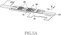
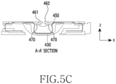
- FIG. 5A is a perspective view illustrating a hinge housing 430 in which a flexible printed circuit board 450 and a hinge plate 460 are disposed.
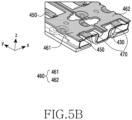
- FIG. 5B is a cross-sectional perspective view of the hinge housing 430, taken along line A-A' of FIG. 5A .
- FIG. 5C is a cross-sectional view of the hinge housing 430, taken along line A-A' of FIG. 5A .
- a first hinge plate 461 and a second hinge plate 462 may be connected with each other to be foldable by a hinge structure.
- an electronic device for example, the electronic device 40 of FIG. 4
- one surface of the first hinge plate 461 and one surface of the second hinge plate 462 may face each other.
- one surface of the first hinge plate 461 and one surface of the second hinge plate 462 may face in the same direction (for example, a +z axis).
- the flexible printed circuit board 450 may be disposed in a direction (for example, an x-axis direction) perpendicular to a folding axis (or rotation axis) (for example, a y-axis direction) of the electronic device 40.
- the flexible printed circuit board 450 may cross over the first hinge plate 461 and the second hinge plate 462 which are disposed on both sides of the hinge housing 430.
- the arrangement direction of the flexible printed circuit board 450 is not necessarily limited to the direction (for example, the x-axis direction) perpendicular to the folding axis.
- the hinge plate 460 may be coupled with the hinge housing 430. According to an embodiment, the hinge plate 460 may have at least one guide hole 470 formed thereon. At least part of the flexible printed circuit board 450 may be inserted into an inner space of the hinge housing through the guide hole 470, or at least part may be removed from the inside of the hinge housing. The guide hole 470 may guide a movement of the flexible printed circuit board 450 when the electronic device 40 is folded.
- At least part of the flexible printed circuit board 450 may be inserted into the guide hole 479, and an area of the flexible printed circuit board 450 that is inserted into the guide hole 470 may move in a direction toward the front surface of the electronic device 40 (for example, the +z axis direction) when the electronic device 40 is folded.
- at least part of the flexible printed circuit board 450 may be exposed to one surface of the first hinge plate 461 or one surface of the second hinge plate 462 through the guide hole 470.
- the flexible printed circuit board 450 when the electronic device 40 is in a folded state, at least part of the flexible printed circuit board 450 may be disposed in an inner space of the hinge housing 430.
- the flexible printed circuit board 450 may be disposed in a direction from the first hinge plate 461 to the second hinge plate 462 across a space formed by the hinge housing 430 and a display layer 480.
- At least part of the flexible printed circuit board 450 that is disposed in the inner space of the hinge housing 430 may be removed from the space through the guide hole 470 of the first hinge plate 461 and the second hinge plate 462.
- the flexible printed circuit board 450 extended toward the first hinge plate 461 and the second hinge plate 462 may be extended to a main printed circuit board of the electronic device 40.
- the flexible printed circuit board 450 may have one end electrically connected with a first printed circuit board disposed in a first housing (for example, the first housing 410 of FIG. 4 ), and the other end electrically connected with a second printed circuit board disposed in a second housing (for example, the second housing 420 of FIG. 4 ).
- the flexible printed circuit board 450 may be fixed to one surface of the hinge plate 460. As described above, at least part of the flexible printed circuit board 450 may be inserted into the hinge housing through the guide holes 470, such that the flexible printed circuit board 450 is primarily fixed.
- the flexible printed circuit board 450 may further be fixed secondarily by a fixing structure formed on the flexible printed circuit board and a fixing member formed on the hinge plate 460.
- FIG. 6 is a cross-sectional view illustrating a flexible printed circuit board 450 in a flat state or a folded state of an electronic device 40 according to an embodiment, respectively.
- FIG. 6 (a) illustrates a flat state of the electronic device 40 and FIG. 6 (b) illustrates a folded state of the electronic device 40.
- the electronic device 40 and the flexible printed circuit board 450 may be referred to by the electronic device 40 and the flexible printed circuit board 450 of FIGS. 4 and 5 .
- the same reference numerals are used and a redundant explanation will be omitted.
- the flexible printed circuit board 450 may include a first section 451 and a second section 452 which is extended from one side of the first section 451.
- the configuration of the flexible printed circuit board is not limited thereto.
- the flexible printed circuit board 450 may omit at least one section of the above-described sections or may further include at least one other section.
- the flexible printed circuit board 450 may include a third section 453 extended from the other side of the first section 451.
- the flexible printed circuit board 450 may be symmetrical with reference to the third section 453. However, this should not be considered as limiting the invention.
- a shape of at least part of the flexible printed circuit board 450 may be changed according to whether the electronic device is in the folded state or flat state (i.e., unfolded state).
- the second section 452 of the flexible printed circuit board 450 may be bent (may have a curved shape or may have a curved cross section), and, when the electronic device 40 is in the flat state, the second section 452 may be unbent (may have a flat shape or may have a linear cross section.
- the third section 453 may be disposed to correspond to a folding area of the electronic device 40.
- the third section 453 when the electronic device 40 is in the flat state (i.e., open state), the third section 453 may be disposed in a space formed by the hinge housing 430 and the display layer 480 (including a first display layer 481 and a second display layer 482) or the hinge plate 460.
- the third section 453 may include a linear area at least part of which has a flat surface.
- the third section 453 may refer to a section that maintains its shape even when the electronic device 40 is both in the folded state and flat state.
- the third section 453 may refer to a section that maintains a linear shape (or a flat shape) when the electronic device 40 is in the folded state or flat state.
- the flexible printed circuit board 450 may include a first connection section 451a extended from one side of the third section 453, and a second connection section 451b extended from the other side of the third section 453.
- the first connection section 451a may include the first section 451 which is extended from the one side of the third section 453, and the second section 452 which is extended from one side of the first section 451.
- the flexible printed circuit board 450 is not limited thereto.
- the first connection section 451a of the flexible printed circuit board 450 may further include at least one section extended from one side of the second section 452.
- the first section 451 may include a curved portion which has a curvature.
- the first section 451 may include a shape that is bent from one side of the third section 453 in a folding direction (for example, a +z axis direction) of the electronic device 40.
- the first section 451 may include a curved surface which is seamlessly formed between the third section 453 and the second section 452.
- the first section 451 may refer to a section that maintains its curved shape when the electronic device 40 is changed from folded to unfolded, and vice versa.
- the first section 451 may refer to a section that maintains a curved shape having a curvature even when the electronic device 40 is folded or unfolded.
- the second section 452 may refer to a section the shape of which is changed when the electronic device 40 is changed from folded to unfolded, and vice versa.
- the second section 452 of the flexible printed circuit board 450 may be bent or unbent when the electronic device 40 is folded or unfolded.
- the second section 452 may refer to a section that forms a linear area at least part of which is a flat surface in the folded state of the electronic device 40, and forms a curved surface having a curvature in the flat state of the electronic device 40.
- a variance in the curvature of the second section 452 when the electronic device 40 is changed from the flat state to the folded state, a variance in the curvature of the second section 452 may be greater than a variance in the curvature of the first section 451.
- a variance in the curvature of the second section 452 when a first housing (for example, the first housing 410 of FIG. 4 ) and a second housing (for example, the second housing 420 of FIG. 4 ) rotate through a hinge structure, a variance in the curvature of the second section 452 may be greater than a variance in the curvature of the first section 451.
- a repulsive force generated by elasticity according to bending of the second section 452 of the flexible printed circuit board 450 may be greater than a repulsive force of the first section 451 due to the variance difference. Since the second section 452 is less bent than the first section 451 due to the greater repulsive force, the curvature of the second section 452 which is bent in the flat state of the electronic device as shown in FIG. 6A may be smaller than the curvature of the first section 451 in the flat state. Accordingly, since the variance in the curvature of the second section 452 caused by folding and unfolding of the electronic device 40 is reduced, the second section 452 may effectively prevent a damage to the flexible printed circuit board 450 occurring by repeated folding of the electronic device 40.
- FIG. 7 is a top view of a flexible printed circuit board 750 according to an embodiment.
- the flexible printed circuit board 750 may be referred to by the flexible printed circuit board 450 of FIGS. 4 to 6 . Regarding components which are the same as or substantially the same as those described above, a redundant explanation will be omitted.
- the flexible printed circuit board 750 may include a third section 753, a first section 751 extended from one side and/or the other side of the third section 753, and a second section 752 extended from one side of the first section 751.
- the flexible printed circuit board 750 may include a fixing area 760 to be fixed to an electronic device (for example, the electronic device 40 of FIG. 4 ).
- the fixing area 760 of the flexible printed circuit board 750 may include a first fixing structure 761 fixed to a first hinge plate (for example, the first hinge plate 461 of FIG. 5 ), and a second fixing structure 762 fixed to a second hinge plate (for example, the second hinge plate 462 of FIG. 5 ).
- the flexible printed circuit board 750 may omit or further include at least one fixing structure.
- the flexible printed circuit board 750 may further include a third fixing structure which is opposite to the first fixing structure 761 with reference to the flexible printed circuit board 750, and a fourth fixing structure which is opposite to the second fixing structure 762 with reference to the flexible printed circuit board 750.
- the fixing area 760 may be disposed to be perpendicular to a longitudinal direction (for example, an x-axis direction) of the flexible printed circuit board 750.
- the fixing area 760 may be disposed to face in the same direction as a rotation axis (or folding axis) direction (for example, a y-axis direction) of a hinge structure of an electronic device (for example, the electronic device 40 of FIG. 4 ).
- the arrangement direction of the fixing area 760 is not necessarily limited to the direction (for example, the y-axis direction) perpendicular to the longitudinal direction of the flexible printed circuit board 750 or to the same direction as the rotation axis of the hinge structure.
- widths of sections of the flexible printed circuit board 750 may be different from one another.
- the width may refer to a length in the direction perpendicular to the longitudinal direction (for example, the x-axis direction) of the flexible printed circuit board 750.
- the width may refer to a rotation axis direction (for example, the y-axis direction) of the hinge structure of the electronic device 40.
- the rotation axis direction may refer to a direction of penetrating through the rotation axis of the hinge structure.
- a width DB of the second section 752 of the flexible printed circuit board 750 may be larger than a width DA of the first section 751. That is, a length (i.e., width DB) of the second section 752 of the flexible printed circuit board 750 in the rotation axis direction (for example, the y-axis direction) of the hinge structure may be longer than a length (i.e., width DA) of the first section 751 in the rotation axis direction. Accordingly, a repulsive force of the second section 752 generated by elasticity according to bending of the flexible printed circuit board 750 may be greater than a repulsive force of the first section 751.
- the width DB of the second section 752 is larger than the width DA of the first section 751, a stress of the second section 752 may be greater than a stress of the first section 751. Due to the difference in the stress between the first section 751 and the second section 752, the flexible printed circuit board 750 may be bent with the curvature of the second section 752 being smaller than the curvature of the first section 751 when the electronic device is unfolded and the flexible printed circuit board 750 is bent. Accordingly, the second section 752 the curvature of which is changed more greatly than the first section 751 according to bending of the flexible printed circuit board may be effectively prevented from being damaged.
- a width DC of the third section 753 of the flexible printed circuit board 750 may be larger than each of the width DA of the first section 751 and the width DB of the second section 752.
- a length of the third section 753 of the flexible printed circuit board 750 in the rotation axis direction (for example, the y-axis direction) of the hinge structure may be longer than the length of each of the first section 751 and the second section 752.
- FIG. 8 is a cross-sectional view and a top view illustrating a flexible printed circuit board according to an embodiment.
- the flexible printed circuit board 850 may be referred to by the flexible printed circuit board 450 of FIGS. 4 to 6 , and the flexible printed circuit board 750 of FIG. 7 . Regarding components which are the same as or substantially the same as those described above, a redundant explanation will be omitted.
- the flexible printed circuit board 850 may further include a linear section 854 which is disposed between a first section 851 and a second section 852.
- the linear section 854 may be a section that is included in the first section 851.
- widths of the sections of the flexible printed circuit board 820 may be different from one another.
- the width may refer to a length of the flexible printed circuit board 850 in a longitudinal direction (for example, an x-axis direction).
- the width may refer to a length along a surface of the flexible printed circuit board 850 in a direction from one end of the flexible printed circuit board 850 that is connected with a first printed circuit board disposed in a first housing (for example, the first housing 410 of FIG. 4 ) to the other end of the flexible printed circuit board 850 that is connected with a second printed circuit board disposed in a second housing (for example, the second housing 420 of FIG. 4 ).
- a width WB of the second section 852 of the flexible printed circuit board 850 may be larger than a width WA of the first section 851.
- a length (i.e., WB) of the second section 852 of the flexible printed circuit board 850 in the longitudinal direction (e.g., x axis direction) of the flexible printed circuit board 850 may be longer than a length (i.e., WA) of the first section 851. Accordingly, a repulsive force of the second section 852 generated by elasticity according to bending of the flexible printed circuit board 850 may be greater than a repulsive force of the first section 851.
- the second section 852 Since the width WB of the second section 852 is larger than the width WA of the first section 851, the second section 852 may be bent or unbent over a larger section. Accordingly, the second section 852 the curvature of which is changed more greatly than the first section 851 according to bending of the flexible printed circuit board may be effectively prevented from being damaged.
- a width WC of a third section 853 of the flexible printed circuit board 850 may be larger than each of the width WA of the first section 851 and the width WB of the second section 852. That is, a length of the third section 853 of the flexible printed circuit board 850 in the longitudinal direction (for example, the x-axis direction) of the flexible printed circuit board 850 may be longer than the length of each of the first section 851 and the second section 852.
- FIG. 9 is a top view illustrating a flexible printed circuit board 950 including at least one of a stiffener 910 or a coating layer according to an embodiment.
- the flexible printed circuit board 950 may be referred to by the flexible printed circuit board 450 of FIGS. 4 to 6 , the flexible printed circuit board 750 of FIG. 7 , and the flexible printed circuit board 850 of FIG. 8 . Regarding components which are the same as or substantially the same as those described above, a redundant explanation will be omitted.
- thicknesses of sections of the flexible printed circuit board 950 may be different from one another.
- the "thickness" is measured in a direction normal to a plane of the flexible printed circuit board (e.g., the z direction).
- a thickness of a second section 952 of the flexible printed circuit board 950 may be thicker than a thickness of a first section 951. Accordingly, a repulsive force of the second section 952 generated by elasticity according to bending of the flexible printed circuit board 950 may be greater than a repulsive force of the first section 951.
- the thickness of the second section 952 is thicker than the thickness of the first section 951, a stress of the second section 952 may be greater than a stress of the first section 951. Due to the difference in the stress between the first section 951 and the second section 952, the flexible printed circuit board 950 may be bent with the curvature of the second section 952 being smaller than the curvature of the first section 951 when the electronic device is unfolded and the flexible printed circuit board 950 is bent. Accordingly, the second section 952 the curvature of which is changed more greatly than the first section 951 according to bending of the flexible printed circuit board 950 may be effectively prevented from being damaged.
- a thickness of a third section 953 of the flexible printed circuit board 950 may be thicker than the thickness of each of the first section 951 and the second section 952. Accordingly, a repulsive force of the third section 953 generated by elasticity according to bending of the flexible printed circuit board 950 may be greater than a repulsive force of each of the first section 951 or the second section 952.
- the second section 952 of the flexible printed circuit board 950 may further include at least one of at least one stiffener 910 or at least one coating layer than the first section 951.
- the at least one of at least one stiffener 910 or at least one coating layer may be stacked in the thickness direction. Accordingly, the thickness of the second section 952 may be thicker than the thickness of the first section 951.
- the second section 952 further includes at least one of the stiffener 910 or the coating layer than the first section 951, such that a repulsive force of the second section 952 generated by elasticity according to bending of the flexible printed circuit board 950 is greater than a repulsive force of the first section 951.
- the stiffener 910 may include at least one high-polymer layer.
- the stiffener 910 may include at least one of polyimide (PI) or plastic.
- the coating layer may include an electro-magnetic interference (EMI) coating layer.
- EMI electro-magnetic interference
- the third section 953 of the flexible printed circuit board 950 may further include at least one of the stiffener 910 or the coating layer than at least one of the first section 951 or the second section 952. Accordingly, the thickness of the third section 953 may be thicker than the thickness of at least one of the first section 951 or the second section 952.
- FIG. 10 is a top view illustrating a flexible printed circuit board including a stiffener or a coating layer according to another embodiment.
- the flexible printed circuit board 1050 may be referred to by the flexible printed circuit board 450 of FIGS. 4 to 6 and the flexible printed circuit board 750, 850, 950 of FIGS. 7 to 9 . Regarding components which are the same as or substantially the same as those described above, a redundant explanation will be omitted.
- a length of a second section 1052 in a longitudinal direction (for example, an x-axis direction) of the flexible printed circuit board 1050 is not long or an area of the second section 1052 is small when the flexible printed circuit board 1050 is mass-produced, it may not be easy to dispose a stiffener or to coat a coating layer on the second section 1052. Accordingly, an area that includes the second section 1052 or an area that is adjacent to the second section 1052 may further include a stiffener or a coating layer.
- a thickness of an area 1054 between a first section 1051 and a fixing area 1060 may be thicker than a thickness of the first section 1051.
- the area 1054 may be an area that includes the second section 1052.
- the flexible printed circuit board 1050 may further include at least one of at least one stiffener 1010 or at least one coating layer in the area 1054 between the first section 1051 and the fixing area 1060.
- the stiffener 1010 may include at least one high-polymer layer.
- the stiffener 1010 may include at least one of polyimide (PI) or plastic.
- the coating layer may include an electro-magnetic interference (EMI) coating layer.
- EMI electro-magnetic interference
- the area 1054 between the first section 1051 and the fixing area 1060 may further include at least one of the stiffener 1010 or the coating layer than the first section 1051, such that a repulsive force of the area 1054 generated by elasticity according to bending of the flexible printed circuit board 1050 is greater than a repulsive force of the first section 1051. Since the area 1054 is less bent than the first section 1051 due to the greater repulsive force, the curvature of the area 1054 which is bent in the flat state of the electronic device may be smaller than the curvature of the first section 1051.
- the area 1054 the curvature of which is changed more greatly than the first section 1051 according to bending of the flexible printed circuit board may be effectively prevented from being damaged.
- FIG. 11 is a top view of a flexible printed circuit board according to an embodiment.
- the flexible printed circuit board 1150 may be referred to by the flexible printed circuit board 450 of FIGS. 4 to 6 and the flexible printed circuit board 750, 850, 950, 1050 of FIGS. 7 to 10 . Regarding components which are the same as or substantially the same as those described above, a redundant explanation will be omitted.
- the flexible printed circuit board 1150 may include a first area 1101 in which a stress generated according to bending or unbending of the flexible printed circuit board 1150 is relatively great, a fixing area 1103 which is extended from one side of the first area 1101, a second area 1102 which is extended from one side of the fixing area 1103, and a third area 1104, 1105 which is connected with a printed circuit board.
- the flexible printed circuit board 1150 may omit at least one of the above-described areas or may further include at least one other area.
- a thickness of the first area 1101 may be thicker than a thickness of the second area 1102.
- the first area 1101 may further include at least one of a stiffener or a coating layer than the second area 1102.
- the first area 1101 may further include at least one high-polymer layer than the second area 1102.
- the stiffener may include at least one of polyimide (PI) or plastic.
- the coating layer may include an electro-magnetic interference (EMI) coating layer.
- EMI electro-magnetic interference
- At least one of the first area 1101 or the third area 1105 may further include at least one metal layer.
- at least one of the first area 1101 or the third area 1105 may include a steel use stainless (SUS) layer.
- SUS steel use stainless
- At least one of the fixing area 1103 or the third area 1104, 1105 may further include at least one resin layer than the first area 1101 or the second area 1102.
- at least one of the fixing area 1103 or the third area 1104, 1105 may further include a prepreg than the first area 1101 or the second area 1102.
- At last one of the third area 1104 or the second area 1102 may further include a protection layer than at least one of the first area 1101 or the fixing area 1103.
- a protection layer than at least one of the first area 1101 or the fixing area 1103.
- FIG. 12 is a cross-sectional view illustrating a flat state or a folded state of an electronic device 120 including a flexible printed circuit board 1250 according to another embodiment, respectively.
- the electronic device 120 may be referred to by the electronic device 10 of FIGS. 1 to 3 . Regarding components which are the same as or substantially the same as those described above, a redundant explanation will be omitted.
- the electronic device 120 may include a hinge housing 1230 including a hinge structure, a first hinge plate 1241 disposed in the hinge housing 1230, a second hinge plate 1242 disposed on an upper side of the first hinge plate 1241, and a flexible printed circuit board 1250 disposed between the first hinge plate 1241 and the second hinge plate 1242.
- the configuration of the electronic device 120 is not limited thereto.
- the electronic device 120 may omit at least one component of the above-described components or may further include at least one other component.
- a shape of at least part of the flexible printed circuit board 1250 may be changed when the electronic device 120 is folded or unfolded.
- the flexible printed circuit board 1250 may include a first section 1251, a second section 1252 extended from one side of the first section, and a third section 1253 extended from one side of the second section 1252.
- the configuration of the flexible printed circuit board 1250 is not limited thereto.
- the flexible printed circuit board 1250 may omit at least one section of the above-described sections or may further include at least one other section.
- the flexible printed circuit board 1250 may include a fourth section extended from the other side of the first section 1251.
- the flexible printed circuit board 1250 may include the fourth section 1254, a first extension portion 1251a extended from one side of the fourth section 1254, and a second extension portion 1251b extended from the other side of the fourth section 1254.
- the first extension portion 1251a may include the first section 1251, the second section 1252, and the third section 1253.
- the first extension portion 1251a and the second extension portion 1251b may be symmetric with reference to the fourth section 1254. However, this should not be considered as limiting the invention.
- the first section 1251 may have its shape changed when the electronic device 120 is folded or unfolded.
- at least one of the first section 1251, the second section 1252, or the third section 1253 may be bent or unbent when the electronic device 120 is folded or unfolded.
- the first section 1251 may include a curved shape which is formed seamlessly in the folded state of the electronic device 120.
- the folded state of the electronic device 120 at least part of the first section 1251 may be bent in a direction in which a housing of the electronic device 120 in the folded state faces (for example, +z axis direction).
- the first section 1251 may be bent in a direction in which the electronic device is unfolded (for example, a -x-axis direction) in the flat state of the electronic device 120.
- the first section 1251 in the flat state of the electronic device 120, may include a curved surface which is convex in a direction in which the front surface of the electronic device faces (for example, a +z-axis direction).
- the second section 1252 may be unbent in the folded state of the electronic device 120.
- the second section 1252 in the folded state of the electronic device 120, the second section 1252 may include a linear area at least part of which is flat. At least part of the second section 1252 may be bent in the flat state of the electronic device 120.
- the second section 1252 may include a curved surface which is convex in a direction in which the rear surface of the electronic device faces (for example, a -z-axis direction).
- the third section 1253 may be unbent in the folded state of the electronic device 120.
- the third section 1253 in the folded state of the electronic device 120, may include a linear area at least part of which is flat. At least part of the third section 1253 may be bent in the flat state of the electronic device 120.
- the third section 1253 may include a curved surface which is convex in the direction in which the front surface of the electronic device faces (for example, the +z-axis direction).
- a variance in the curvature of the first section 1251 when the electronic device 40 is folded, a variance in the curvature of the first section 1251 may be greater than a variance in the curvature of the second section 1252 or the third section 1253.
- a variance in the curvature of the first section 1251 when a first housing (for example, the first housing 410 of FIG. 4 ) and a second housing (for example, the second housing 420 of FIG. 4 ) rotate through a hinge structure, a variance in the curvature of the first section 1251 may be greater than a variance in the curvature of the second section 1252 or the third section 1253.
- a width of the first section 1251 of the flexible printed circuit board 1250 may be larger than a width of the second section 1252 or the third section 1253.
- a length of the first section 1251 of the flexible printed circuit board 1250 in a rotation axis direction (for example, a y-axis direction) of the hinge structure may be longer than a length of the second section 1252 or the third section 1253. Accordingly, a repulsive force of the first section 1251 generated by elasticity according to bending of the flexible printed circuit board 1250 may be greater than a repulsive force of the second section 1252 or the third section 1253.
- the width of the first section 1251 is larger than the width of the second section 1252 or the third section 1253, a stress of the first section 1251 may be greater than a stress of the second section 1252 or the third section 1253. Due to the difference in the stress between the first section 1251 and the second section 1252 or the third section 1253, the flexible printed circuit board 1250 may be bent with the curvature of the first section 1251 being smaller than the curvature of the second section 1252 or the third section 1253 when the electronic device is unfolded and the flexible printed circuit board 1250 is bent. Accordingly, the first section 1251 the curvature of which is changed more greatly than the second section 1252 or the third section 1253 according to bending of the flexible printed circuit board may be effectively prevented from being damaged.
- the width of the first section 1251 of the flexible printed circuit board 1250 may be larger than each of the width of the second section 1252 and the third section 1253.
- a length of the first section 1251 of the flexible printed circuit board 1250 in a longitudinal direction (for example, an x-axis direction) of the flexible printed circuit board 1250 may be longer than a length of each of the second section 1252 and the third section 1253. Accordingly, a repulsive force of the first section 1251 generated by elasticity according to bending of the flexible printed circuit board 1250 may be greater than a repulsive force of each of the second section 1252 and the third section 1253.
- the flexible printed circuit board 1250 may be bent with the curvature of the first section 1251 being smaller than the curvature of the second section 1252 or the third section 1253 when the electronic device is unfolded and the flexible printed circuit board 1250 is bent. Accordingly, the first section 1251 the curvature of which is changed more greatly than the second section 1252 or the third section 1253 according to bending of the flexible printed circuit board 1250 may be effectively prevented from being damaged.
- a thickness of the first section 1251 of the flexible printed circuit board 1250 may be thicker than a thickness of each of the second section 1252 and the third section 1253. Accordingly, a repulsive force of the first section 1251 generated by elasticity according to bending of the flexible printed circuit board 1250 may be greater than a repulsive force of each of the second section 1252 and the third section 1253. Since the first section 1251 is less bent than the second section 1252 or the third section 1253 due to the greater repulsive force, the curvature of the first section 1251 which is bent in the flat state of the electronic device 120 may be smaller than the curvature of the second section 1252 or the third section 1253.
- the thickness of the first section 1251 may be thicker than the thickness of each of the second section 1252 and the third section 1253, such that a variance in the curvature of the first section 1251 caused by folding and unfolding of the electronic device 120 is reduced. Accordingly, the first section 1251 the curvature of which is changed more greatly than the second section 1252 or the third section 1253 according to bending of the flexible printed circuit board may be effectively prevented from being damaged.
- the flexible printed circuit board 1250 may further include at least one of at least one stiffener or at least one coating layer than the second section 1252 or the third section 1253. Accordingly, the thickness of the first section 1251 may be thicker than the thickness of the second section 1252 or the third section 1253.
- the first section 1251 further includes at least one of a stiffener or a coating layer than the second section 1252 or the third section 1253, such that a repulsive force of the first section 1251 generated by elasticity according to bending of the flexible printed circuit board 1250 is greater than a repulsive force of the second section 1252 or the third section 1253.
- the curvature of the first section 1251 which is bent in the flat state of the electronic device 120 may be smaller than the curvature of the second section 1252 or the third section 1253. Accordingly, the first section 1251 the curvature of which is changed more greatly than the second section 1252 or the third section 1253 according to bending of the flexible printed circuit board may be effectively prevented from being damaged.
- an electronic device may include: a hinge structure, which is a folding area and includes a hinge housing; a first housing connected to the hinge structure; a second housing connected with the first housing through the hinge structure to be rotatable with respect to the first housing; and a flexible printed circuit board (FPCB), which has a first end connected to a first printed circuit board (PCB) disposed in the first housing, and a second end connected to a second PCB disposed in the second housing.
- a hinge structure which is a folding area and includes a hinge housing
- a first housing connected to the hinge structure
- a second housing connected with the first housing through the hinge structure to be rotatable with respect to the first housing
- FPCB flexible printed circuit board
- the FPCB may include a first section and a second section, and the second section may be extended from a first side of the first section, and a variance in a curvature of the second section may be greater than a variance in a curvature of the first section when the first housing and the second housing rotate with respect to the hinge structure, and a repulsive force of the second section generated by elasticity according to folding of the second section may be greater than a repulsive force of the first section.
- a length of the second section of the FPCB in a rotation axial direction of the hinge structure may be longer than a length of the first section in the rotation axial direction.
- a length of the second section of the FPCB in a direction along a surface of the FPCB from the one end connected with the first PCB to the second end connected with the second PCB is longer than a length of the first section in the same direction.
- a thickness of the second section of the FPCB may be thicker than a thickness of the first section.
- the second section of the FPCB may further include at least one of a stiffener or a coating layer than the first section, and the stiffener may include at least one high-polymer layer.
- the FPCB may further include a third section which is extended from a second side of the first section, and includes a linear area at least part of which has a flat surface, where the second side of the first section is opposite the first side.
- the third section of the FPCB may further include at least one of a stiffener or a coating layer than the first section or the second section, and the stiffener may include at least one high-polymer layer.
- a thickness of the third section of the FPCB may be thicker than a thickness of at least one of the first section or the second section.
- a length of the third section of the FPCB in a rotation axial direction of the hinge structure may be longer than a length of each of the first section and the second section in the rotation axial direction.
- the electronic device may further include a first hinge plate disposed in the first housing and a second hinge plate disposed in the second housing
- the FPCB may further include at least one fixing area which is disposed on one side of the second section and is fixed to the first hinge plate or the second hinge plate.
- the FPCB may further include at least one of a stiffener or a coating layer between the first section and the fixing area, and the stiffener may include at least one high-polymer layer.
- an electronic device may include: a hinge structure, which is a folding area and includes a hinge housing; a first housing connected to the hinge structure; a second housing connected with the first housing through the hinge structure to be rotatable with respect to the first housing; and an FPCB, which has a first end connected to a first PCB disposed in the first housing, and a second end connected to a second PCB disposed in the second housing, and the FPCB may include: a first section including a curvature when the first housing and the second housing are folded or unfolded through the hinge structure; and a second section, which is extended from a first side of the first section, and is disposed to form a linear area at least part of which has a flat surface in the folded state of the first housing and the second housing, and to form a curvature in the unfolded state, a variance in a curvature of the second section may be greater than a variance in a curvature of the first section when the first housing and the second housing
- a length of the second section of the FPCB in a rotation axial direction of the hinge structure may be longer than a length of the first section in the rotation axial direction.
- a length of the second section of the FPCB in a direction along a surface of the FPCB from the first end connected with the first PCB to the second end connected with the second PCB may be longer than a length of the first section in the same direction.
- a thickness of the second section of the FPCB may be thicker than a thickness of the first section.
- the second section of the FPCB may further include at least one of a stiffener or a coating layer than the first section, and the stiffener may include at least one high-polymer layer.
- the FPCB may further include a third section which is extended from a second side of the first section, and includes a linear area at least part of which has a flat surface, where the second side of the first section is opposite the first side.
- the third section of the FPCB may further include at least one of a stiffener or a coating layer than the first section or the second section, and the stiffener may include at least one high-polymer layer.
- a thickness of the third section of the FPCB may be thicker than a thickness of at least one of the first section or the second section.
- an electronic device may include: a hinge structure which is a folding area and includes a hinge housing; a first housing connected to the hinge structure; a second housing connected with the first housing through the hinge structure to be rotatable with respect to the first housing; and an FPCB, which has a first end connected to a first PCB disposed in the first housing, and a second end connected to a second PCB disposed in the second housing, and the FPCB may include a first section, a second section, and a third section, the second section is extended from one side of the first section, and the third section is extended from one side of the second section and is disposed, a variance in a curvature of the first section is greater than a variance in a curvature of at least one of the second section or the third section when the first housing and the second housing rotate with respect to the hinge structure, and a repulsive force of the first section generated by elasticity according to folding of the first section may be greater than a repulsive force of at
Landscapes
- Engineering & Computer Science (AREA)
- Computer Hardware Design (AREA)
- Theoretical Computer Science (AREA)
- Microelectronics & Electronic Packaging (AREA)
- Physics & Mathematics (AREA)
- Human Computer Interaction (AREA)
- General Engineering & Computer Science (AREA)
- General Physics & Mathematics (AREA)
- Mathematical Physics (AREA)
- Computer Networks & Wireless Communication (AREA)
- Signal Processing (AREA)
- Telephone Set Structure (AREA)
Applications Claiming Priority (3)
| Application Number | Priority Date | Filing Date | Title |
|---|---|---|---|
| KR20210132569 | 2021-10-06 | ||
| KR1020210181826A KR20230049521A (ko) | 2021-10-06 | 2021-12-17 | 연성 회로기판을 포함하는 전자 장치 |
| PCT/KR2022/014865 WO2023059018A1 (ko) | 2021-10-06 | 2022-10-04 | 연성 회로기판을 포함하는 전자 장치 |
Publications (2)
| Publication Number | Publication Date |
|---|---|
| EP4380137A1 true EP4380137A1 (de) | 2024-06-05 |
| EP4380137A4 EP4380137A4 (de) | 2024-11-27 |
Family
ID=85803566
Family Applications (1)
| Application Number | Title | Priority Date | Filing Date |
|---|---|---|---|
| EP22878839.4A Pending EP4380137A4 (de) | 2021-10-06 | 2022-10-04 | Elektronische vorrichtung mit flexibler leiterplatte |
Country Status (3)
| Country | Link |
|---|---|
| US (1) | US12513823B2 (de) |
| EP (1) | EP4380137A4 (de) |
| WO (1) | WO2023059018A1 (de) |
Families Citing this family (3)
| Publication number | Priority date | Publication date | Assignee | Title |
|---|---|---|---|---|
| KR102727844B1 (ko) * | 2019-12-23 | 2024-11-08 | 삼성전자주식회사 | 디스플레이를 포함하는 폴더블 전자 장치 |
| USD1029781S1 (en) * | 2021-12-10 | 2024-06-04 | Samsung Electronics Co., Ltd. | Electronic device |
| USD1029782S1 (en) * | 2021-12-10 | 2024-06-04 | Samsung Electronics Co., Ltd. | Electronic device |
Family Cites Families (16)
| Publication number | Priority date | Publication date | Assignee | Title |
|---|---|---|---|---|
| US9516743B2 (en) * | 2013-02-27 | 2016-12-06 | Apple Inc. | Electronic device with reduced-stress flexible display |
| KR20160103083A (ko) * | 2013-12-24 | 2016-08-31 | 폴리에라 코퍼레이션 | 탈부착형 2차원 플렉서블 전자 기기용 지지 구조물 |
| KR102323593B1 (ko) * | 2014-07-23 | 2021-11-17 | 엘지이노텍 주식회사 | 광원 모듈 및 이를 구비한 표시 모듈 |
| JP6622048B2 (ja) * | 2015-10-05 | 2019-12-18 | ソニーモバイルコミュニケーションズ株式会社 | 電子機器 |
| KR102426694B1 (ko) | 2017-05-02 | 2022-07-29 | 삼성전자주식회사 | 플렉서블 디스플레이를 포함하는 전자 장치 |
| EP3806591B1 (de) | 2018-07-17 | 2023-04-26 | Huawei Technologies Co., Ltd. | Mobiles endgerät |
| KR102575550B1 (ko) | 2018-08-20 | 2023-09-07 | 삼성전자주식회사 | 굴곡부를 포함하는 인쇄 회로 기판 및 이를 포함하는 전자 장치 |
| KR102731698B1 (ko) | 2018-12-28 | 2024-11-15 | 엘지디스플레이 주식회사 | 플렉서블 디스플레이 장치 및 이를 포함하는 전자 기기 |
| KR102588997B1 (ko) | 2019-02-18 | 2023-10-13 | 삼성전자 주식회사 | 배선 부재 고정 구조를 포함하는 전자 장치 |
| KR102765539B1 (ko) | 2019-05-03 | 2025-02-12 | 삼성전자주식회사 | 탄성 부재를 포함하는 전자 장치 |
| CN112134970B (zh) | 2019-06-24 | 2021-08-13 | 华为技术有限公司 | 一种可折叠电子设备 |
| KR102834211B1 (ko) | 2019-10-25 | 2025-07-15 | 삼성디스플레이 주식회사 | 표시 장치 |
| JP7447523B2 (ja) | 2020-02-07 | 2024-03-12 | ニデック株式会社 | 光学ユニット |
| JP7281105B2 (ja) * | 2020-11-20 | 2023-05-25 | カシオ計算機株式会社 | 連結体、バンド、および時計 |
| CN213847328U (zh) * | 2021-07-05 | 2021-07-30 | 荣耀终端有限公司 | 折叠屏设备 |
| KR20230040174A (ko) | 2021-09-15 | 2023-03-22 | 삼성전자주식회사 | 연성 인쇄 회로 기판을 포함하는 폴더블 전자 장치 |
-
2022
- 2022-10-04 WO PCT/KR2022/014865 patent/WO2023059018A1/ko not_active Ceased
- 2022-10-04 EP EP22878839.4A patent/EP4380137A4/de active Pending
-
2023
- 2023-07-05 US US18/346,880 patent/US12513823B2/en active Active
Also Published As
| Publication number | Publication date |
|---|---|
| US12513823B2 (en) | 2025-12-30 |
| EP4380137A4 (de) | 2024-11-27 |
| WO2023059018A1 (ko) | 2023-04-13 |
| US20230354524A1 (en) | 2023-11-02 |
Similar Documents
| Publication | Publication Date | Title |
|---|---|---|
| US12513823B2 (en) | Electronic device including flexible printed circuit board | |
| JP7712986B2 (ja) | 折りたたみ式ディスプレイを含む携帯用通信装置 | |
| US12072744B2 (en) | Hinge structure and electronic device including the same | |
| EP3472822B1 (de) | Elektronische vorrichtung mit einer flexiblen anzeige | |
| EP3428770B1 (de) | Flexible elektronische vorrichtung | |
| US10491987B2 (en) | Electronic device including flexible housing | |
| US10306783B2 (en) | Foldable electronic device including flexible display | |
| KR102308940B1 (ko) | 방수 구조를 포함하는 전자 장치 | |
| US20240163356A1 (en) | Foldable display and electronic device comprising same | |
| CN108781503B (zh) | 具有射频扼流圈的柔性印刷电路 | |
| EP3324604A1 (de) | Elektronische vorrichtung mit wasserdichter struktur | |
| KR102444053B1 (ko) | 차폐 구조를 구비하는 전자 장치 | |
| KR20190101600A (ko) | 금속 플레이트를 포함하는 커넥터 및 이를 포함하는 전자 장치 | |
| KR20230049521A (ko) | 연성 회로기판을 포함하는 전자 장치 | |
| US20150169092A1 (en) | Sensor panel, touch panel and electronic device | |
| KR102745243B1 (ko) | 접착부를 포함하는 전자 장치 | |
| KR102714097B1 (ko) | 하우징 구조물을 포함하는 전자 장치 | |
| US20240237245A1 (en) | Electronic device comprising display support member | |
| CN118056395A (zh) | 包括柔性电路板的电子装置 | |
| KR20190115347A (ko) | 커넥터 및 이를 포함하는 전자 장치 | |
| US12348930B2 (en) | Electronic apparatus | |
| EP4529141A1 (de) | Elektronische vorrichtung mit stützelement | |
| KR20250080689A (ko) | 연성회로기판을 포함하는 전자 장치 | |
| KR20250015563A (ko) | 플렉서블 디스플레이를 포함하는 전자 장치 | |
| KR20240025300A (ko) | 전자 장치 |
Legal Events
| Date | Code | Title | Description |
|---|---|---|---|
| STAA | Information on the status of an ep patent application or granted ep patent |
Free format text: STATUS: THE INTERNATIONAL PUBLICATION HAS BEEN MADE |
|
| PUAI | Public reference made under article 153(3) epc to a published international application that has entered the european phase |
Free format text: ORIGINAL CODE: 0009012 |
|
| STAA | Information on the status of an ep patent application or granted ep patent |
Free format text: STATUS: REQUEST FOR EXAMINATION WAS MADE |
|
| 17P | Request for examination filed |
Effective date: 20240228 |
|
| AK | Designated contracting states |
Kind code of ref document: A1 Designated state(s): AL AT BE BG CH CY CZ DE DK EE ES FI FR GB GR HR HU IE IS IT LI LT LU LV MC ME MK MT NL NO PL PT RO RS SE SI SK SM TR |
|
| A4 | Supplementary search report drawn up and despatched |
Effective date: 20241028 |
|
| RIC1 | Information provided on ipc code assigned before grant |
Ipc: G06F 1/16 20060101ALI20241022BHEP Ipc: H05K 1/02 20060101ALI20241022BHEP Ipc: H05K 1/14 20060101ALI20241022BHEP Ipc: H04M 1/02 20060101AFI20241022BHEP |
|
| DAV | Request for validation of the european patent (deleted) | ||
| DAX | Request for extension of the european patent (deleted) | ||
| STAA | Information on the status of an ep patent application or granted ep patent |
Free format text: STATUS: EXAMINATION IS IN PROGRESS |
|
| 17Q | First examination report despatched |
Effective date: 20251002 |
|
| GRAP | Despatch of communication of intention to grant a patent |
Free format text: ORIGINAL CODE: EPIDOSNIGR1 |
|
| STAA | Information on the status of an ep patent application or granted ep patent |
Free format text: STATUS: GRANT OF PATENT IS INTENDED |
|
| INTG | Intention to grant announced |
Effective date: 20260303 |