EP4380335A1 - Procédé de fabrication d'une cellule photovoltaïque en pérovskite - Google Patents
Procédé de fabrication d'une cellule photovoltaïque en pérovskite Download PDFInfo
- Publication number
- EP4380335A1 EP4380335A1 EP22210577.7A EP22210577A EP4380335A1 EP 4380335 A1 EP4380335 A1 EP 4380335A1 EP 22210577 A EP22210577 A EP 22210577A EP 4380335 A1 EP4380335 A1 EP 4380335A1
- Authority
- EP
- European Patent Office
- Prior art keywords
- perovskite
- layer
- providing
- charge transport
- transport layer
- Prior art date
- Legal status (The legal status is an assumption and is not a legal conclusion. Google has not performed a legal analysis and makes no representation as to the accuracy of the status listed.)
- Pending
Links
Images




Classifications
-
- H—ELECTRICITY
- H10—SEMICONDUCTOR DEVICES; ELECTRIC SOLID-STATE DEVICES NOT OTHERWISE PROVIDED FOR
- H10K—ORGANIC ELECTRIC SOLID-STATE DEVICES
- H10K71/00—Manufacture or treatment specially adapted for the organic devices covered by this subclass
- H10K71/10—Deposition of organic active material
- H10K71/12—Deposition of organic active material using liquid deposition, e.g. spin coating
-
- H—ELECTRICITY
- H10—SEMICONDUCTOR DEVICES; ELECTRIC SOLID-STATE DEVICES NOT OTHERWISE PROVIDED FOR
- H10F—INORGANIC SEMICONDUCTOR DEVICES SENSITIVE TO INFRARED RADIATION, LIGHT, ELECTROMAGNETIC RADIATION OF SHORTER WAVELENGTH OR CORPUSCULAR RADIATION
- H10F10/00—Individual photovoltaic cells, e.g. solar cells
- H10F10/10—Individual photovoltaic cells, e.g. solar cells having potential barriers
- H10F10/14—Photovoltaic cells having only PN homojunction potential barriers
-
- H—ELECTRICITY
- H10—SEMICONDUCTOR DEVICES; ELECTRIC SOLID-STATE DEVICES NOT OTHERWISE PROVIDED FOR
- H10F—INORGANIC SEMICONDUCTOR DEVICES SENSITIVE TO INFRARED RADIATION, LIGHT, ELECTROMAGNETIC RADIATION OF SHORTER WAVELENGTH OR CORPUSCULAR RADIATION
- H10F10/00—Individual photovoltaic cells, e.g. solar cells
- H10F10/10—Individual photovoltaic cells, e.g. solar cells having potential barriers
- H10F10/17—Photovoltaic cells having only PIN junction potential barriers
-
- H—ELECTRICITY
- H10—SEMICONDUCTOR DEVICES; ELECTRIC SOLID-STATE DEVICES NOT OTHERWISE PROVIDED FOR
- H10F—INORGANIC SEMICONDUCTOR DEVICES SENSITIVE TO INFRARED RADIATION, LIGHT, ELECTROMAGNETIC RADIATION OF SHORTER WAVELENGTH OR CORPUSCULAR RADIATION
- H10F10/00—Individual photovoltaic cells, e.g. solar cells
- H10F10/10—Individual photovoltaic cells, e.g. solar cells having potential barriers
- H10F10/19—Photovoltaic cells having multiple potential barriers of different types, e.g. tandem cells having both PN and PIN junctions
-
- H—ELECTRICITY
- H10—SEMICONDUCTOR DEVICES; ELECTRIC SOLID-STATE DEVICES NOT OTHERWISE PROVIDED FOR
- H10F—INORGANIC SEMICONDUCTOR DEVICES SENSITIVE TO INFRARED RADIATION, LIGHT, ELECTROMAGNETIC RADIATION OF SHORTER WAVELENGTH OR CORPUSCULAR RADIATION
- H10F77/00—Constructional details of devices covered by this subclass
- H10F77/10—Semiconductor bodies
- H10F77/12—Active materials
-
- H—ELECTRICITY
- H10—SEMICONDUCTOR DEVICES; ELECTRIC SOLID-STATE DEVICES NOT OTHERWISE PROVIDED FOR
- H10K—ORGANIC ELECTRIC SOLID-STATE DEVICES
- H10K30/00—Organic devices sensitive to infrared radiation, light, electromagnetic radiation of shorter wavelength or corpuscular radiation
- H10K30/10—Organic devices sensitive to infrared radiation, light, electromagnetic radiation of shorter wavelength or corpuscular radiation comprising heterojunctions between organic semiconductors and inorganic semiconductors
-
- H—ELECTRICITY
- H10—SEMICONDUCTOR DEVICES; ELECTRIC SOLID-STATE DEVICES NOT OTHERWISE PROVIDED FOR
- H10K—ORGANIC ELECTRIC SOLID-STATE DEVICES
- H10K30/00—Organic devices sensitive to infrared radiation, light, electromagnetic radiation of shorter wavelength or corpuscular radiation
- H10K30/10—Organic devices sensitive to infrared radiation, light, electromagnetic radiation of shorter wavelength or corpuscular radiation comprising heterojunctions between organic semiconductors and inorganic semiconductors
- H10K30/15—Sensitised wide-bandgap semiconductor devices, e.g. dye-sensitised TiO2
-
- H—ELECTRICITY
- H10—SEMICONDUCTOR DEVICES; ELECTRIC SOLID-STATE DEVICES NOT OTHERWISE PROVIDED FOR
- H10K—ORGANIC ELECTRIC SOLID-STATE DEVICES
- H10K30/00—Organic devices sensitive to infrared radiation, light, electromagnetic radiation of shorter wavelength or corpuscular radiation
- H10K30/20—Organic devices sensitive to infrared radiation, light, electromagnetic radiation of shorter wavelength or corpuscular radiation comprising organic-organic junctions, e.g. donor-acceptor junctions
- H10K30/211—Organic devices sensitive to infrared radiation, light, electromagnetic radiation of shorter wavelength or corpuscular radiation comprising organic-organic junctions, e.g. donor-acceptor junctions comprising multiple junctions, e.g. double heterojunctions
-
- H—ELECTRICITY
- H10—SEMICONDUCTOR DEVICES; ELECTRIC SOLID-STATE DEVICES NOT OTHERWISE PROVIDED FOR
- H10K—ORGANIC ELECTRIC SOLID-STATE DEVICES
- H10K30/00—Organic devices sensitive to infrared radiation, light, electromagnetic radiation of shorter wavelength or corpuscular radiation
- H10K30/40—Organic devices sensitive to infrared radiation, light, electromagnetic radiation of shorter wavelength or corpuscular radiation comprising a p-i-n structure, e.g. having a perovskite absorber between p-type and n-type charge transport layers
-
- H—ELECTRICITY
- H10—SEMICONDUCTOR DEVICES; ELECTRIC SOLID-STATE DEVICES NOT OTHERWISE PROVIDED FOR
- H10K—ORGANIC ELECTRIC SOLID-STATE DEVICES
- H10K30/00—Organic devices sensitive to infrared radiation, light, electromagnetic radiation of shorter wavelength or corpuscular radiation
- H10K30/50—Photovoltaic [PV] devices
-
- H—ELECTRICITY
- H10—SEMICONDUCTOR DEVICES; ELECTRIC SOLID-STATE DEVICES NOT OTHERWISE PROVIDED FOR
- H10K—ORGANIC ELECTRIC SOLID-STATE DEVICES
- H10K30/00—Organic devices sensitive to infrared radiation, light, electromagnetic radiation of shorter wavelength or corpuscular radiation
- H10K30/80—Constructional details
- H10K30/81—Electrodes
- H10K30/82—Transparent electrodes, e.g. indium tin oxide [ITO] electrodes
-
- H—ELECTRICITY
- H10—SEMICONDUCTOR DEVICES; ELECTRIC SOLID-STATE DEVICES NOT OTHERWISE PROVIDED FOR
- H10K—ORGANIC ELECTRIC SOLID-STATE DEVICES
- H10K30/00—Organic devices sensitive to infrared radiation, light, electromagnetic radiation of shorter wavelength or corpuscular radiation
- H10K30/80—Constructional details
- H10K30/84—Layers having high charge carrier mobility
- H10K30/85—Layers having high electron mobility, e.g. electron-transporting layers or hole-blocking layers
-
- H—ELECTRICITY
- H10—SEMICONDUCTOR DEVICES; ELECTRIC SOLID-STATE DEVICES NOT OTHERWISE PROVIDED FOR
- H10K—ORGANIC ELECTRIC SOLID-STATE DEVICES
- H10K30/00—Organic devices sensitive to infrared radiation, light, electromagnetic radiation of shorter wavelength or corpuscular radiation
- H10K30/80—Constructional details
- H10K30/84—Layers having high charge carrier mobility
- H10K30/86—Layers having high hole mobility, e.g. hole-transporting layers or electron-blocking layers
-
- H—ELECTRICITY
- H10—SEMICONDUCTOR DEVICES; ELECTRIC SOLID-STATE DEVICES NOT OTHERWISE PROVIDED FOR
- H10K—ORGANIC ELECTRIC SOLID-STATE DEVICES
- H10K71/00—Manufacture or treatment specially adapted for the organic devices covered by this subclass
- H10K71/40—Thermal treatment, e.g. annealing in the presence of a solvent vapour
-
- H—ELECTRICITY
- H10—SEMICONDUCTOR DEVICES; ELECTRIC SOLID-STATE DEVICES NOT OTHERWISE PROVIDED FOR
- H10K—ORGANIC ELECTRIC SOLID-STATE DEVICES
- H10K71/00—Manufacture or treatment specially adapted for the organic devices covered by this subclass
- H10K71/60—Forming conductive regions or layers, e.g. electrodes
-
- H—ELECTRICITY
- H10—SEMICONDUCTOR DEVICES; ELECTRIC SOLID-STATE DEVICES NOT OTHERWISE PROVIDED FOR
- H10K—ORGANIC ELECTRIC SOLID-STATE DEVICES
- H10K85/00—Organic materials used in the body or electrodes of devices covered by this subclass
- H10K85/50—Organic perovskites; Hybrid organic-inorganic perovskites [HOIP], e.g. CH3NH3PbI3
-
- H—ELECTRICITY
- H10—SEMICONDUCTOR DEVICES; ELECTRIC SOLID-STATE DEVICES NOT OTHERWISE PROVIDED FOR
- H10K—ORGANIC ELECTRIC SOLID-STATE DEVICES
- H10K85/00—Organic materials used in the body or electrodes of devices covered by this subclass
- H10K85/20—Carbon compounds, e.g. carbon nanotubes or fullerenes
- H10K85/211—Fullerenes, e.g. C60
-
- H—ELECTRICITY
- H10—SEMICONDUCTOR DEVICES; ELECTRIC SOLID-STATE DEVICES NOT OTHERWISE PROVIDED FOR
- H10K—ORGANIC ELECTRIC SOLID-STATE DEVICES
- H10K85/00—Organic materials used in the body or electrodes of devices covered by this subclass
- H10K85/60—Organic compounds having low molecular weight
-
- H—ELECTRICITY
- H10—SEMICONDUCTOR DEVICES; ELECTRIC SOLID-STATE DEVICES NOT OTHERWISE PROVIDED FOR
- H10K—ORGANIC ELECTRIC SOLID-STATE DEVICES
- H10K85/00—Organic materials used in the body or electrodes of devices covered by this subclass
- H10K85/60—Organic compounds having low molecular weight
- H10K85/615—Polycyclic condensed aromatic hydrocarbons, e.g. anthracene
- H10K85/624—Polycyclic condensed aromatic hydrocarbons, e.g. anthracene containing six or more rings
-
- H—ELECTRICITY
- H10—SEMICONDUCTOR DEVICES; ELECTRIC SOLID-STATE DEVICES NOT OTHERWISE PROVIDED FOR
- H10K—ORGANIC ELECTRIC SOLID-STATE DEVICES
- H10K85/00—Organic materials used in the body or electrodes of devices covered by this subclass
- H10K85/60—Organic compounds having low molecular weight
- H10K85/631—Amine compounds having at least two aryl rest on at least one amine-nitrogen atom, e.g. triphenylamine
- H10K85/633—Amine compounds having at least two aryl rest on at least one amine-nitrogen atom, e.g. triphenylamine comprising polycyclic condensed aromatic hydrocarbons as substituents on the nitrogen atom
-
- H—ELECTRICITY
- H10—SEMICONDUCTOR DEVICES; ELECTRIC SOLID-STATE DEVICES NOT OTHERWISE PROVIDED FOR
- H10K—ORGANIC ELECTRIC SOLID-STATE DEVICES
- H10K85/00—Organic materials used in the body or electrodes of devices covered by this subclass
- H10K85/60—Organic compounds having low molecular weight
- H10K85/649—Aromatic compounds comprising a hetero atom
- H10K85/653—Aromatic compounds comprising a hetero atom comprising only oxygen as heteroatom
-
- H—ELECTRICITY
- H10—SEMICONDUCTOR DEVICES; ELECTRIC SOLID-STATE DEVICES NOT OTHERWISE PROVIDED FOR
- H10K—ORGANIC ELECTRIC SOLID-STATE DEVICES
- H10K85/00—Organic materials used in the body or electrodes of devices covered by this subclass
- H10K85/60—Organic compounds having low molecular weight
- H10K85/649—Aromatic compounds comprising a hetero atom
- H10K85/657—Polycyclic condensed heteroaromatic hydrocarbons
- H10K85/6572—Polycyclic condensed heteroaromatic hydrocarbons comprising only nitrogen in the heteroaromatic polycondensed ring system, e.g. phenanthroline or carbazole
-
- Y—GENERAL TAGGING OF NEW TECHNOLOGICAL DEVELOPMENTS; GENERAL TAGGING OF CROSS-SECTIONAL TECHNOLOGIES SPANNING OVER SEVERAL SECTIONS OF THE IPC; TECHNICAL SUBJECTS COVERED BY FORMER USPC CROSS-REFERENCE ART COLLECTIONS [XRACs] AND DIGESTS
- Y02—TECHNOLOGIES OR APPLICATIONS FOR MITIGATION OR ADAPTATION AGAINST CLIMATE CHANGE
- Y02E—REDUCTION OF GREENHOUSE GAS [GHG] EMISSIONS, RELATED TO ENERGY GENERATION, TRANSMISSION OR DISTRIBUTION
- Y02E10/00—Energy generation through renewable energy sources
- Y02E10/50—Photovoltaic [PV] energy
- Y02E10/549—Organic PV cells
Definitions
- the present invention relates to the field of photovoltaic devices. More particularly, it relates to a method of manufacture of a perovskite-based photovoltaic cell.
- PV devices photovoltaic devices
- perovskite absorber layers have been showing promise as an alternative or complement to conventional crystalline and thin-film silicon-based PV devices.
- Perovskites are organometallic halide materials with a formula generically written as ABX 3 , where A is an inorganic or organic cation such as Cs, CH 3 NH 3 or HC(NH 2 ) 2 , B is a metal such as tin or lead, and X is a halogen atom such as iodine, bromine or chlorine.
- methylammonium lead trihalide (CH 3 NH 3 PbX 3 ), Caesium formamidinum lead trihalide (CsH 2 NCHNH 2 PbX 3 ), and methylammonium tin triiodide (CH3NH3SnI3).
- These compounds adopt a similar crystal structure to calcium titanium oxide (CaTiO 3 ) and, when illuminated, generate electron-hole pairs, which can be separated by sandwiching the perovskite absorber layer between an electron transporting n-type layer and a hole-transporting p-type layer, with the perovskite serving as the intrinsic (i) layer so as to form a PIN or NIP junction, analogous to its silicon counterpart.
- Such perovskite-based cells can be used as single-junction cells, or can be combined with a silicon cell to create a tandem PV device, the perovskite junction being located on the light-incident side of the cell.
- the perovskite layer itself is typically deposited in a wet process, such as wet coating followed by evaporation of the carrier solvent, although vapour deposition techniques are also showing promise.
- An example of room-temperature solution deposition of perovskite is disclosed in Liu & Kelly, "Perovskite solar cells with a planar heterojunction structure prepared using room-temperature solution processing techniques", Nature Photonics 8, 133-138 (2014 ).
- Perovskite solar cells are typically limited in performance by i) charge carrier transport losses occurring within the perovskite absorber when reaching a perovskite layer thickness approaching the micrometre scale (that is on the same order of magnitude as the electron and hole diffusion lengths), and ii) by defects that form at the interfaces between the perovskite and the charge carrier selective layers. These voltage losses can be mitigated i) by adapting deposition conditions to yield a perovskite microstructure exhibiting large grains that span across the full perovskite layer thickness, and ii) by developing surface-treatment materials that coordinate with the perovskite surface defects and hence passivate them.
- the microstructure of the perovskite layer can be tuned using a variety of approaches, from fine-tuning the deposition conditions to the use of growth-modulating agents in the perovskite deposition process.
- the passivation of surface defects is typically achieved by a separate processing step treat an already existing perovskite layer.
- Document CN113629196 describes a method of depositing perovskite layers in which phosphonic acids are incorporated in a FA 0.85 Cs 0.15 PbI 3 perovskite precursor solution applied to the underlying layer of the PV cell by a 1-step spin coating approach as part of the fabrication of an n-i-p configuration photovoltaic cell, followed by annealing for 20 minutes at a temperature of 200°C.
- the approach enables stabilizing the photoactive FA 0.85 Cs 0.15 PbI 3 and leads to a chemical modification of the bulk of the perovskite, as highlighted by a shift in bandgap and a larger light absorption range.
- the relatively high curing temperature used is not suitable for a wide range of perovskite materials as it may lead to their decomposition, which is undesirable.
- the aim of the present invention is hence to at least partially overcome the limitations of the prior art.
- the invention relates to a method of manufacturing a solar cell, as defined in independent claim 1.
- This method comprises at least steps of (further intermediate steps not being excluded):
- said step of providing a perovskite-based light absorber layer comprises:
- said first charge transport layer is a hole selective layer comprising one of:
- said second charge transport layer typically comprises carbon-60.
- said additive comprises one or more of: 2,3,4,5,6-pentafluorobenzylphosphonic acid, benzylphosphonic acid, 4-bromobenzylphosphonic acid, 4-fluorobenzylphosphonic acid, (4-chlorophenyl)phosphonic acid, phenylphosphonic acid.
- said perovskite-based light-absorber layer has a thickness between 200 nm and 2000 nm, preferably from 500 to 1500 nm.
- said perovskite-based light absorber layer comprises (Cs,FA,MA)Pb(I,Br,Cl) 3 or (Cs,FA)Pb(I,Br,Cl) 3 , preferably Cs 0.18 FA 0.82 Pb(I,Br) 3 .
- said perovskite precursor solution comprises organic and inorganic perovskite precursors and is applied directly to said first charge transport layer, i.e. as a single-step deposition.
- these precursors such as lead halides (PbI 2 , PbBr 2 , PbCl 2 ), cesium halide (Csl, CsBr, CsCI), formamidinium halides (FAI, FABr, FACI) and methylammonium halides (MAI, MABr, MACI), of which PbI 2 , FAI, PbBr 2 , FABr, MABr and CsI are preferred) are known to the skilled person and depend on the type of perovskite used for the perovskite-based light absorber layer.
- the concentration of said additive in said perovskite precursor solution is preferably 0.1-50 mMol, preferably between 1 and 10 mMol.
- said substrate may have a roughness of less than 1 ⁇ m Ra on a surface facing said perovskite-based light absorber layer.
- step of providing a perovskite-based light absorber layer comprises a step of vapour depositing a layer of CsX and/or PbX 2 , where X is I, Br or Cl directly or indirectly on said first charge transport layer followed by said step of applying said perovskite precursor solution.
- said perovskite precursor solution comprises organic perovskite precursors (such as those mentioned above) and is exempt from inorganic perovskite precursors since these were already deposited in the vapour deposition step.
- said substrate may have a roughness of 0 ⁇ m to 10 ⁇ m Ra, preferably 2 ⁇ m to 10 ⁇ m Ra on a surface facing said perovskite-based light absorber layer.
- concentration of said additive in said perovskite precursor solution may be from 0.1 mMol to 50 mMol.
- FIG. 1 schematically illustrates a solar cell 1 (i.e. a photovoltaic cell) produced by the method of the invention.
- This can be a single junction perovskite cell, in which case substrate 3 is an opaque or transparent support layer such as glass or metal, or a tandem cell, in which substrate 3 is a bottom cell such as (but not limited to) a conventional silicon cell such as a crystalline silicon cell.
- the upper surface of the substrate 3 may be textured, as is generally known and which will be discussed further below.
- each layer can be directly deposited on the previously-formed layer, or may be indirectly deposited thereupon with an intervening layer in between, and the method proceeds from bottom to top in the orientation of figure 1 .
- the cell 1 Upon the substrate 3, the cell 1 comprises a first transparent conductive oxide layer 5, such as indium tin oxide (ITO), zinc oxide, indium zinc oxide (IZO) or similar.
- First transparent conductive oxide layer 5 may be doped or undoped.
- a first charge transport layer 7 is deposited. This is either a hole transport (p-type) or an electron transport (n-type) layer, of an applicable type as is generally known in the field of perovskite photovoltaic cells.
- HTL hole transport layer
- spiro-TTB (2,2',7,7'-Tetra(N,N-di-p-tolyl)amino-9,9-spirobifluorene)
- TaTM (1,3,4,6-Tetra-O-acetyl-2-O-(trifluoromethanesulfonyl)-beta-D-mannopyranose)
- Me-4PACz (4-(3,6- dimethyl-9H-carbazol-9-yl)butyl]phosphonic acid), -[2-(3,6-dimethoxy-9H-carbazol-9-yl)ethyl]phosphonic acid (MeO-2PACz) or [2-(9H-carbazol-9-yl)ethyl]phosphonic acid (2PACz) are typically used.
- perovskite layer 9 Upon the first charge transport layer is deposited a perovskite-based light absorber layer 9 (which can be abbreviated to "perovskite layer 9" in the context of the present specification), the deposition of which forms the key to the invention as will become more apparent below.
- This perovskite is typically based on the generic formulae (Cs,FA,MA)Pb(I,Br,Cl) 3 or (Cs,FA)Pb(I,Br,Cl) 3 .
- Other types of perovskite material are however possible.
- This is typically an electron transport layer (ETL) based on carbon-60.
- second charge transport layer 11 Upon second charge transport layer 11 is deposited a second layer of transparent conductive oxide 13, which may be a single layer or a multilayer of two different materials, such as one or more of doped or undoped tin oxide, indium tin oxide, indium zinc oxide or similar.
- a patterned metallic contact layer 15 which may comprise is screen-printed silver paste, vapour-deposited copper, or similar, and is typically patterned.
- a further layer 17 (or indeed layers), such as antireflection layers, can also be deposited on top of the second layer of transparent conductive oxide 13 in the interstices between the patterned metallic contacts 15.
- a non-illustrated buffer layer of e.g. atomic layer deposited SnO 2 may be deposited between the second charge transport layer 12 and the second layer of transparent conductive oxide 13.
- This layer 9 is deposited either in a one-step solution deposition process, or in a two-step process such as that described in F. Sahli, J. Werner, B. A. Kamino, M. B Hurninger, R. Monnard, B. Paviet-Salomon, L. Barraud, L. Ding, J. J. Diaz Leon, D. Sacchetto, G. Cattaneo, M. Despeisse, M. Boccard, S. Nicolay, Q. Jeangros, B. Niesen, C. Ballif, "Fully textured monolithic perovskite/silicon tandem solar cells with 25.2% power conversion efficiency", Nat. Mater.
- This two-step process involves a first step of co-evaporating a CsBr/PbI 2 template 9a directly or indirectly on the underlying layer, namely the first charge transport layer 7, and then solution-depositing the perovskite precursor 9b so as to form the perovskite layer 9.
- PbX 2 lead halides
- CsX I, Br or Cl
- FAX formamidinium halides
- MAX methylammonium halides
- 3-7 mMol, further typically substantially 5 mMol additive concentration is used for one-step and two-step depositions.
- the phosphonic acid or phosphonate salt is dissolved in one or more of a combination of polar and non-polar solvents (such as dimethylformamide (DMF) or dimethylsulfoxide (DMSO), or ethanol) and is added to the perovskite precursors (or, in the case of two-step deposition processes, only to the organic perovskite precursors) up to the desired concentration.
- polar and non-polar solvents such as dimethylformamide (DMF) or dimethylsulfoxide (DMSO), or ethanol
- Such phosphonic acids have the general formula R-PO 3 H 2 , where R is any fully or partially fluorinated or non-fluorinated organic functional groups/molecules.
- R is any fully or partially fluorinated or non-fluorinated organic functional groups/molecules.
- a typical example which has shown good results is 2,3,4,5,6-pentafluorobenzylphosphonic acid (FBPAc), but other similar molecules are also possible, such as benzylphosphonic acid, 4-bromobenzylphosphonic acid, 4-fluorobenzylphosphonic acid, (4-chlorophenyl)phosphonic acid and phenylphosphonic acid.
- FBPAc 2,3,4,5,6-pentafluorobenzylphosphonic acid
- benzylphosphonic acid 4-bromobenzylphosphonic acid
- 4-fluorobenzylphosphonic acid 4-fluorobenzylphosphonic acid
- (4-chlorophenyl)phosphonic acid and phenylphosphonic acid.
- R 1 -PO(OR 2 )(OR 3 ) R 1 is again any fully or partially fluorinated or non-fluorinated organic functional groups/molecules
- R 2 and R 3 are a cation such as H + , Cs + , K + or FA + (i.e. a formamidinium cation).
- the solvent is allowed to evaporate and the perovskite layer is annealed in ambient or inert gas environment at a temperature of between 100°C and 170°C, preferably between 140°C and 150°C.
- the resulting final perovskite layer 9 thickness is between 200 nm and 2000 nm, preferably between 500 nm and 1500 nm.
- the former works best with a relatively lightly-textured underlying surface (i.e. the free surface of the first charge transport layer 7), with a roughness typically less than 1 ⁇ m Ra.
- the two-step deposition process provides good results with relatively large textures, of the order of 1-10 ⁇ m Ra.
- the additive tunes the growth of the perovskite layer 9, and segregates on the free surface of this layer during its crystallization to passivate defects and mitigate non-radiative surface recombination losses.
- ITO substrates were first coated with a hole transport layer 7 (HTL), namely spiro-TTB, TaTM or Me-4PACz. These three materials were selected based on their compatibility with textured surfaces as the first two can be thermally evaporated, while the self-assembling properties (on ITO) of the latter should yield a conformal coating on textured surfaces.
- a CsBr/PbI 2 template was co-evaporated on glass/ITO substrate, before spin coating an organo-halide solution (consisting of FABr and FAI in various ratios, in some cases with FBPAc).
- a thermal annealing step in ambient conditions at 150 °C then converted the films into a perovskite phase.
- a perovskite composition with an optical Eg of -1.70 eV was selected.
- Figure 2 is a graph of quasi Fermi-level splitting (QFLS) of bare perovskite layers deposited on glass, on a spiro-TTB HTL 7, on a TaTm HTL 7, and on a Me-4PACz HTL 7 (labelled as HTL losses, empty diamonds), both with and without FBPAc additive during solution deposition of the perovskite layer 9, and both with and without a C60 ETL 11 on the perovskite layer (indicated as HTL + ETL losses, filled diamonds).
- the data is extracted from photoluminescence quantum yield (PLQY) data. This graph clearly shows that QFLS remains substantially constant when incorporating an FBPAc additive.
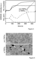
- grazing-incident wide-angle X-ray scattering (GIWAXS) was performed in situ at 150 °C to understand the impact of FBPAc on the perovskite crystallization process. While the crystallization onset of the perovskite (110) and (002) (q ⁇ 10.1 nm -1 ) planes is similar with or without the additive, FBPAc then slows down the perovskite crystallization after 100 s at 150 °C, as showed in figure 4 .
- Perovskite films were then included in 0.25-cm 2 glass/ITO/HTL/perovskite/C 60 /BCP(or SnO 2 )/Cu (or Ag) single junctions to validate with current-voltage (J-V) measurements the improvements induced by FBPAc.
- J-V current-voltage
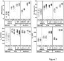
- the open circuit voltage (V oc ) of the devices improves by 20-30 mV when switching from spiro-TTB to TaTm and Me-4PACz, and by 40-50 mV extra when adding FBPAc.
- the corresponding fill factor (FF) also increases on average from -69 % to -76 % when changing the HTL 7 and then to -78-81 % with the additive.
- PCE power conversion efficiency
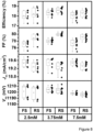
- Varying the concentration of FBPAc from 2.5 mM to 7.5 mM in the FABr:FAI solution does not affect the performance significantly with a HTL 7 made of Me-4PACz, as shown in figure 8 .
- perovskite deposition conditions were then adapted to produce 1-cm 2 tandem solar cells on silicon heterojunction (SHJ) bottom cells serving as base layers 3 featuring pyramids of 2-3 ⁇ m height on both sides and a recombination junction on the front side.
- Perovskite layer 9 was made thicker (from -400 nm in single-junctions to -1 ⁇ m) to reach current matching conditions in a tandem with Si with a perovskite Eg of -1.7 eV.
- a CsBr/PbI 2 template of 660 nm thickness was deposited and the spin coating parameters were adapted accordingly.
- the front electrode was made transparent by switching to a stack made of C60 (layer 11), SnOx (lower part of layer 13), indium zinc oxide (IZO) (upper part of layer 13), a Ag grid (layer 15), and a MgF2 antireflective coating (layer 17).
- a V oc of 1.9V could be obtained with either TaTM or Me-4PACz, in line with single-junction and QFLS data.
- the FF of TaTm-based tandems was however significantly lower than with Me-4PACz ( ⁇ 70% compared to >75%), likely as a result of the low hole mobility in undoped TaTm.
- a tandem cell 1 as described above featuring Me-4PACz as HTL 7 and FBPAc as additive in the perovskite precursor solution was sent to the National Renewable Energy Laboratory (NREL) for certification.
- NREL National Renewable Energy Laboratory
- This tandem was slightly top-cell limited and both sub-cells produced a Jsc >20 mA/cm 2 .
- the stabilized J-V properties of the device were measured using the asymptotic maximum power (Pmax) scan method in standard test conditions (STC, 25 °C, 1000 W/m2, AM1.5G spectrum).
- the cell reached a V oc of 1.91 V, a Jsc of 20.47 mA/cm2 and a FF of 79.8%, which resulted in a certified PCE of 31.25% (with an aperture area of 1.1677 cm2).
- the method of the invention improves the crystallinity of the perovskite layer 9, which increases the fill factor of the solar cell 1 due to mitigation of charge transport losses within the perovskite layer since the resulting larger grain structure results in fewer grain boundaries along the travel direction of the charge carriers (i.e. perpendicular to the plane of the perovskite layer 9), increasing the cell efficiency.
- the additive passivates the Pb-related defects present at the top surface of the perovskite layer 9 by coordinating with them on this surface, which increases the open circuit voltage of the solar cell 1 while still enabling charge carrier extraction, further increasing the cell efficiency.
- the approach of the invention is versatile and can be implemented in single-junction opaque cells, single-junction semi-transparent cells, and in tandem cells.
Landscapes
- Physics & Mathematics (AREA)
- Electromagnetism (AREA)
- Engineering & Computer Science (AREA)
- Chemical & Material Sciences (AREA)
- Manufacturing & Machinery (AREA)
- Materials Engineering (AREA)
- Inorganic Chemistry (AREA)
- Photovoltaic Devices (AREA)
Priority Applications (3)
| Application Number | Priority Date | Filing Date | Title |
|---|---|---|---|
| EP22210577.7A EP4380335A1 (fr) | 2022-11-30 | 2022-11-30 | Procédé de fabrication d'une cellule photovoltaïque en pérovskite |
| KR1020230168542A KR20240082229A (ko) | 2022-11-30 | 2023-11-28 | 페로브스카이트 광기전력 전지의 제조 방법 |
| US18/523,279 US20240180012A1 (en) | 2022-11-30 | 2023-11-29 | Method of manufacturing a perovskite photovoltaic cell |
Applications Claiming Priority (1)
| Application Number | Priority Date | Filing Date | Title |
|---|---|---|---|
| EP22210577.7A EP4380335A1 (fr) | 2022-11-30 | 2022-11-30 | Procédé de fabrication d'une cellule photovoltaïque en pérovskite |
Publications (1)
| Publication Number | Publication Date |
|---|---|
| EP4380335A1 true EP4380335A1 (fr) | 2024-06-05 |
Family
ID=84536148
Family Applications (1)
| Application Number | Title | Priority Date | Filing Date |
|---|---|---|---|
| EP22210577.7A Pending EP4380335A1 (fr) | 2022-11-30 | 2022-11-30 | Procédé de fabrication d'une cellule photovoltaïque en pérovskite |
Country Status (3)
| Country | Link |
|---|---|
| US (1) | US20240180012A1 (fr) |
| EP (1) | EP4380335A1 (fr) |
| KR (1) | KR20240082229A (fr) |
Citations (2)
| Publication number | Priority date | Publication date | Assignee | Title |
|---|---|---|---|---|
| CN113629196A (zh) | 2021-06-17 | 2021-11-09 | 鲁东大学 | 一种稳定FACs基钙钛矿太阳能电池的制备方法 |
| CN114497426A (zh) * | 2020-10-28 | 2022-05-13 | 南京工业大学 | 一种提高钙钛矿发光二极管亮度的方法及钙钛矿发光二极管 |
Family Cites Families (11)
| Publication number | Priority date | Publication date | Assignee | Title |
|---|---|---|---|---|
| ES2587082T3 (es) * | 2009-12-16 | 2016-10-20 | Heliatek Gmbh | Elemento de construcción fotoactivo con capas orgánicas |
| US10038150B2 (en) * | 2011-02-25 | 2018-07-31 | Ecole Polytechnique Federale De Lausanne (Epfl) | Metal complexes for use as dopants and other uses |
| TWI566449B (zh) * | 2011-11-30 | 2017-01-11 | 諾瓦發光二極體有限公司 | 有機電子裝置及其用途 |
| EP3002801B1 (fr) * | 2014-09-30 | 2018-07-18 | Novaled GmbH | Dispositif électronique organique |
| US10593816B2 (en) * | 2015-01-08 | 2020-03-17 | Korea Research Institute Of Chemical Technology | Method for manufacturing device comprising inorganic/organic hybrid perovskite compound film and device comprising inorganic/organic hybrid perovskite compound film |
| US20180174762A1 (en) * | 2016-12-16 | 2018-06-21 | Uchicago Argonne, Llc | Hybrid organic-inorganic electron selective overlayers for halide perovoskites |
| US11094884B2 (en) * | 2018-01-12 | 2021-08-17 | The Board Of Trustees Of The University Of Alabama | Rapid metal oxide layer-specific photonic treatment using UV LED for fabrication of flexible perovskite structures |
| CN116686423A (zh) * | 2021-02-10 | 2023-09-01 | 高峰 | 器件传输材料组合物的制备方法、组合物、包含其的传输层和包含传输层的电子器件 |
| EP4292144B1 (fr) * | 2021-02-12 | 2026-01-21 | First Solar, Inc. | Matériaux et procédés pour couches de transport de trous dans des dispositifs photovoltaïques à base de pérovskite |
| DE102021201746A1 (de) * | 2021-02-24 | 2022-08-25 | Karlsruher Institut für Technologie | Perowskit-basierte Mehrfachsolarzelle und Verfahren zu ihrer Herstellung |
| EP4145547A1 (fr) * | 2021-09-03 | 2023-03-08 | Saule S.A. | Cellule solaire en pérovskite |
-
2022
- 2022-11-30 EP EP22210577.7A patent/EP4380335A1/fr active Pending
-
2023
- 2023-11-28 KR KR1020230168542A patent/KR20240082229A/ko active Pending
- 2023-11-29 US US18/523,279 patent/US20240180012A1/en active Pending
Patent Citations (2)
| Publication number | Priority date | Publication date | Assignee | Title |
|---|---|---|---|---|
| CN114497426A (zh) * | 2020-10-28 | 2022-05-13 | 南京工业大学 | 一种提高钙钛矿发光二极管亮度的方法及钙钛矿发光二极管 |
| CN113629196A (zh) | 2021-06-17 | 2021-11-09 | 鲁东大学 | 一种稳定FACs基钙钛矿太阳能电池的制备方法 |
Non-Patent Citations (7)
| Title |
|---|
| AKMAN ERDI ET AL: "Moisture-Resistant FAPbI 3 Perovskite Solar Cell with 22.25?% Power Conversion Efficiency through Pentafluorobenzyl Phosphonic Acid Passivation", CHEMSUSCHEM, vol. 14, no. 4, 19 January 2021 (2021-01-19), DE, pages 1176 - 1183, XP093041345, ISSN: 1864-5631, DOI: 10.1002/cssc.202002707 * |
| E. AKMANA. E. SHALANF. SADEGHS. AKIN: "Moisture-Resistant FAPbl3 Perovskite Solar Cell with 22.25 % Power Conversion Efficiency through Pentafluorobenzyl Phosphonic Acid Passivation", CHEMSUSCHEM, vol. 14, 2021, pages 1176 - 1183 |
| F. SAHLIJ. WERNERB. A. KAMINOM. BRAUNINGERR. MONNARDB. PAVIET-SALOMONL. BARRAUDL. DINGJ. J. DIAZ LEOND. SACCHETTO: "Fully textured monolithic perovskite/silicon tandem solar cells with 25.2% power conversion efficiency", NAT. MATER., vol. 17, 2018, pages 820 - 82 |
| HO-BAILLIE ANITA W Y ET AL: "Recent progress and future prospects of perovskite tandem solar cells", APPLIED PHYSICS REVIEWS, AMERICAN INSTITUTE OF PHYSICS, 2 HUNTINGTON QUADRANGLE, MELVILLE, NY 11747, vol. 8, no. 4, 15 October 2021 (2021-10-15), XP012260444, DOI: 10.1063/5.0061483 * |
| LI XIONG ET AL: "Improved performance and stability of perovskite solar cells by crystal crosslinking with alkylphosphonic acid [omega]-ammonium chlorides", NATURE CHEMISTRY, vol. 7, no. 9, 17 August 2015 (2015-08-17), London, pages 703 - 711, XP093041344, ISSN: 1755-4330, DOI: 10.1038/nchem.2324 * |
| SUNG SAE JIN ET AL: "Molecular Engineering for Function-Tailored Interface Modifier in High-Performance Perovskite Solar Cells", ADVANCED ENERGY MATERIALS, vol. 12, no. 27, 30 May 2022 (2022-05-30), DE, pages 2200758, XP093041347, ISSN: 1614-6832, DOI: 10.1002/aenm.202200758 * |
| TOCKORN ET AL.: "Nano-optical designs for high-efficiency monolithic perovskite-silicon tandem solar cells", NATURE NANOTECHNOLOGY, vol. 17, no. 11, pages 1214 - 1221, Retrieved from the Internet <URL:https://doi.org/10.1038/s41565-022-01228-8> |
Also Published As
| Publication number | Publication date |
|---|---|
| KR20240082229A (ko) | 2024-06-10 |
| US20240180012A1 (en) | 2024-05-30 |
Similar Documents
| Publication | Publication Date | Title |
|---|---|---|
| CN112086535B (zh) | 一种叠层电池 | |
| CN116133448B (zh) | 一种钙钛矿-硅基叠层太阳能电池及其制作方法 | |
| US9564593B2 (en) | Solar cells comprising 2d-perovskites | |
| CN114267789B (zh) | 一种同时提高全绒面钙钛矿/晶硅叠层太阳能电池开路电压和稳定性的方法 | |
| Zhou et al. | Solution-processed Cu-doped SnO2 as an effective electron transporting layer for high-performance planar perovskite solar cells | |
| CN107710434A (zh) | 光伏装置 | |
| KR102496459B1 (ko) | 페로브스카이트/갈륨비소 탠덤형 태양 전지 및 이의 제조방법 | |
| US11174276B2 (en) | Organic-inorganic perovskite materials and methods of making the same | |
| CN114335359B (zh) | 一种钙钛矿薄膜的制作方法、太阳能电池和叠层电池 | |
| CN112086534A (zh) | 一种叠层电池及其制作方法 | |
| EP4665124A1 (fr) | Cellule solaire et son procédé de réalisation | |
| WO2023097365A1 (fr) | Cellule photovoltaïque en tandem | |
| US12300446B2 (en) | Multijunction photovoltaic devices with metal oxynitride layer | |
| CN119300618A (zh) | 一种钙钛矿太阳能电池、制备方法及制得的叠层钙钛矿电池 | |
| US20250008755A1 (en) | Perovskite photovoltaic devices and methods of manufacturing thereof | |
| US20240180012A1 (en) | Method of manufacturing a perovskite photovoltaic cell | |
| WO2026020673A1 (fr) | Cellule solaire tandem et procédé de préparation s'y rapportant | |
| CN118678704A (zh) | 太阳能电池及其制备方法、光伏组件、光伏系统 | |
| Sahli et al. | Hybrid sequential deposition process for fully textured perovskite/silicon tandem solar cells | |
| KR102761911B1 (ko) | 탠덤 태양전지의 제조방법 | |
| CN222090033U (zh) | 叠层太阳能电池以及用电装置 | |
| EP4535967A1 (fr) | Perovskite à large bande interdite | |
| Okamoto | Production and efficiency improvement of perovskite solar cells using the new 3-step method | |
| CN122028634A (zh) | 一种B位Cd掺杂二维钙钛矿薄膜及钙钛矿/晶硅叠层太阳能电池 | |
| WO2025207945A1 (fr) | Solutions de précurseur pour cellules solaires en pérovskite |
Legal Events
| Date | Code | Title | Description |
|---|---|---|---|
| PUAI | Public reference made under article 153(3) epc to a published international application that has entered the european phase |
Free format text: ORIGINAL CODE: 0009012 |
|
| STAA | Information on the status of an ep patent application or granted ep patent |
Free format text: STATUS: THE APPLICATION HAS BEEN PUBLISHED |
|
| AK | Designated contracting states |
Kind code of ref document: A1 Designated state(s): AL AT BE BG CH CY CZ DE DK EE ES FI FR GB GR HR HU IE IS IT LI LT LU LV MC ME MK MT NL NO PL PT RO RS SE SI SK SM TR |
|
| STAA | Information on the status of an ep patent application or granted ep patent |
Free format text: STATUS: REQUEST FOR EXAMINATION WAS MADE |
|
| 17P | Request for examination filed |
Effective date: 20241121 |
|
| RBV | Designated contracting states (corrected) |
Designated state(s): AL AT BE BG CH CY CZ DE DK EE ES FI FR GB GR HR HU IE IS IT LI LT LU LV MC ME MK MT NL NO PL PT RO RS SE SI SK SM TR |
|
| RAP3 | Party data changed (applicant data changed or rights of an application transferred) |
Owner name: CSEM CENTRE SUISSE D'ELECTRONIQUE ET DEMICROTECHNIQUE SA - RECHERCHE ET DEVELOPPEMENT |