EP4383039A1 - Circuit de suppression d'alimentation électrique, puce et terminal de communication - Google Patents
Circuit de suppression d'alimentation électrique, puce et terminal de communication Download PDFInfo
- Publication number
- EP4383039A1 EP4383039A1 EP22851937.7A EP22851937A EP4383039A1 EP 4383039 A1 EP4383039 A1 EP 4383039A1 EP 22851937 A EP22851937 A EP 22851937A EP 4383039 A1 EP4383039 A1 EP 4383039A1
- Authority
- EP
- European Patent Office
- Prior art keywords
- power supply
- pmos transistor
- resistor
- low dropout
- dropout regulator
- Prior art date
- Legal status (The legal status is an assumption and is not a legal conclusion. Google has not performed a legal analysis and makes no representation as to the accuracy of the status listed.)
- Pending
Links
Images



Classifications
-
- G—PHYSICS
- G05—CONTROLLING; REGULATING
- G05F—SYSTEMS FOR REGULATING ELECTRIC OR MAGNETIC VARIABLES
- G05F1/00—Automatic systems in which deviations of an electric quantity from one or more predetermined values are detected at the output of the system and fed back to a device within the system to restore the detected quantity to its predetermined value or values, i.e. retroactive systems
- G05F1/10—Regulating voltage or current
- G05F1/46—Regulating voltage or current wherein the variable actually regulated by the final control device is DC
- G05F1/56—Regulating voltage or current wherein the variable actually regulated by the final control device is DC using semiconductor devices in series with the load as final control devices
- G05F1/565—Regulating voltage or current wherein the variable actually regulated by the final control device is DC using semiconductor devices in series with the load as final control devices sensing a condition of the system or its load in addition to means responsive to deviations in the output of the system, e.g. current, voltage, power factor
-
- G—PHYSICS
- G05—CONTROLLING; REGULATING
- G05F—SYSTEMS FOR REGULATING ELECTRIC OR MAGNETIC VARIABLES
- G05F1/00—Automatic systems in which deviations of an electric quantity from one or more predetermined values are detected at the output of the system and fed back to a device within the system to restore the detected quantity to its predetermined value or values, i.e. retroactive systems
- G05F1/10—Regulating voltage or current
- G05F1/46—Regulating voltage or current wherein the variable actually regulated by the final control device is DC
- G05F1/56—Regulating voltage or current wherein the variable actually regulated by the final control device is DC using semiconductor devices in series with the load as final control devices
- G05F1/575—Regulating voltage or current wherein the variable actually regulated by the final control device is DC using semiconductor devices in series with the load as final control devices characterised by the feedback circuit
-
- G—PHYSICS
- G05—CONTROLLING; REGULATING
- G05F—SYSTEMS FOR REGULATING ELECTRIC OR MAGNETIC VARIABLES
- G05F1/00—Automatic systems in which deviations of an electric quantity from one or more predetermined values are detected at the output of the system and fed back to a device within the system to restore the detected quantity to its predetermined value or values, i.e. retroactive systems
- G05F1/10—Regulating voltage or current
- G05F1/46—Regulating voltage or current wherein the variable actually regulated by the final control device is DC
- G05F1/56—Regulating voltage or current wherein the variable actually regulated by the final control device is DC using semiconductor devices in series with the load as final control devices
-
- G—PHYSICS
- G01—MEASURING; TESTING
- G01R—MEASURING ELECTRIC VARIABLES; MEASURING MAGNETIC VARIABLES
- G01R19/00—Arrangements for measuring currents or voltages or for indicating presence or sign thereof
- G01R19/25—Arrangements for measuring currents or voltages or for indicating presence or sign thereof using digital measurement techniques
- G01R19/2506—Arrangements for conditioning or analysing measured signals, e.g. for indicating peak values ; Details concerning sampling, digitizing or waveform capturing
- G01R19/2509—Details concerning sampling, digitizing or waveform capturing
Definitions
- the present invention relates to the field of integrated circuit technologies, and relates to a power supply suppression circuit, and to an integrated circuit chip including the power supply suppression circuit and a corresponding communication terminal.
- a primary technical problem to be solved by the present invention is to provide a power supply suppression circuit.
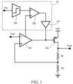
- a power supply suppression circuit including a sampling unit, a compensation unit, and an amplification unit.
- the sampling unit is connected to the compensation unit, and the compensation unit is connected to the amplification unit.
- An enhanced signal in phase with an AC signal on a power supply is generated and outputted to an output end of the error amplification stage of the low dropout regulator, so that a variation of a voltage of an input end of a power output stage of the low dropout regulator closely follows a variation of the power supply voltage, to suppress a voltage outputted by the low dropout regulator from varying with the power supply voltage within the target frequency band.
- the preset sampling node position is any one of a node position an output port of the low dropout regulator, a node position the power supply voltage or a ground cable connected to the low dropout regulator, and a node position on the low dropout regulator where an AC signal of an input end of a power output stage of the low dropout regulator is directly or indirectly controlled.
- the sampling unit includes a second resistor, a third capacitor, a third resistor, a fourth resistor, and a fifth resistor.
- One end of the third resistor is connected to an output port of the low dropout regulator.
- the other end of the third resistor is connected to one end of the third capacitor and one end of the fourth resistor.
- the other end of the third capacitor is connected to one end of the second resistor.
- the other end of the fourth resistor is grounded via the fifth resistor.
- the other end of the second resistor is connected to an input end of the compensation unit.
- the sampling unit includes a sixth resistor and a fourth capacitor.
- One end of the fourth capacitor is connected to a ground cable end connected to the low dropout regulator.
- the other end of the fourth capacitor is connected to one end of the sixth resistor.
- the other end of the sixth resistor is connected to an input end of the compensation unit.
- the amplification unit includes a fourth NMOS transistor and the fifth PMOS transistor.
- a drain end of the fourth NMOS transistor is connected to the drain end of the fifth PMOS transistor and a gate end of a sixth PMOS transistor.
- a gate end of the fourth NMOS transistor is connected to a gate end and a drain end of a second NMOS transistor of the low dropout regulator.
- a source end of the fourth NMOS transistor is grounded.
- the sampling unit includes a seventh resistor and a fifth capacitor.
- One end of the fifth capacitor is connected to the power supply voltage connected to the low dropout regulator.
- the other end of the fifth capacitor is connected to one end of the seventh resistor.
- the other end of the seventh resistor is connected to an input end of the compensation unit.
- the compensation unit is implemented by using a third NMOS transistor.
- a gate end of the third NMOS transistor is connected to an output end of the sampling unit.
- a drain end of the third NMOS transistor is connected to an input end of the amplification unit.
- a source end of the third NMOS transistor is grounded.
- an integrated circuit chip includes the foregoing power supply suppression circuit.
- a communication terminal includes the foregoing power supply suppression circuit.
- an embodiment of the present invention provides a power supply suppression circuit 10, including a sampling unit 105, a compensation unit 106, and an amplification unit 107.
- the sampling unit 105 is connected to the compensation unit 106
- the compensation unit 106 is connected to the amplification unit 107.
- the preset sampling node position of the low dropout regulator to which the sampling unit 105 is connected may be any one of a node position the output port of the low dropout regulator, a node position the power supply voltage or a ground cable connected to the low dropout regulator, and a node position on the low dropout regulator where an AC signal of the input end of the power output stage of the low dropout regulator may be directly or indirectly controlled.
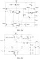
- a first AC signal within a target frequency band is sampled from the output port Vout of the low dropout regulator, and is loaded into the gate end of the fifth PMOS transistor PM24.
- an appropriate amplitude amplification is performed by using a gain loop constituted by the fifth PMOS transistor PM24 and the fourth NMOS transistor NM24 connected in parallel, to enable an amplified signal to be in phase with an AC signal on a power supply.
- the gate end voltage of the sixth PMOS transistor PM25 needs to vary with a source end voltage (that is, the power supply voltage) of the sixth PMOS transistor. If the gate end voltage of the sixth PMOS transistor PM25 can desirably vary with the power supply voltage, the output port Vout of the low dropout regulator does not vary with the power supply voltage.
- FIG. 2b shows a small signal equivalent model of the circuit in FIG. 2a .
- reference ends Vb2 and Vref are noise-free, in other words, are alternating current grounded. Therefore, the PMOS transistors PM20, PM21, and the NMOS transistor NM21 may not be taken into account.
- a capacitor CL and a resistor RL are respectively a load capacitor and a load resistor of the output port Vout of the low dropout regulator.
- a capacitor CL and a resistor RL are respectively a load capacitor and a load resistor of the output port Vout of the low dropout regulator.
- gm n 24 is a small signal gain of the fourth NMOS transistor NM24.
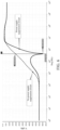
- FIG. 6 shows a simulation result of Embodiment 1.
- a dashed line in the figure is a simulation result of power supply suppression without adding the power supply suppression circuit
- a solid line is a simulation result of power supply suppression after the power supply suppression circuit is added. It may be learned from the simulation results that the power supply suppression circuit can effectively suppress power supply noise within a wide frequency range.
- a frequency point can be selected by adjusting a circuit parameter.
- power supply suppression is improved by about 40 dB compared with an original circuit.
- the sampling unit 105 is connected to a ground cable end connected to the low dropout regulator.
- the sampling unit 105 includes a sixth resistor R32 and a fourth capacitor C32.
- One end of the fourth capacitor C32 is used as an input end of the sampling unit 105, and is configured to be connected to the ground cable end connected to the low dropout regulator.
- the other end of the fourth capacitor C32 is connected to one end of the sixth resistor R32.
- the other end of the sixth resistor R32 is used as an output port of the sampling unit 105, and is configured to be connected to an input end of the compensation unit 106.
- Embodiment 1 to suppress power supply noise within a target frequency band, it is necessary that a variation of a gate end (a PMOS transistor PM35 in FIG. 3 ) voltage of a PMOS transistor of the power output stage of the low dropout regulator closely follows a variation of a power supply voltage within the frequency band. Therefore, an AC current of a PMOS transistor PM34 needs to increase. Due to a voltage dividing function of a PMOS transistor PM33 and an NMOS transistor NM33, a variation of a gate end voltage of the PMOS transistor PM34 closely follows the variation of the power supply voltage.
- Embodiment 1 an implementation idea described in Embodiment 1 is used to shunt an AC current flowing through the NMOS transistor NM33, so that an AC voltage component at a gate end of the PMOS transistor PM34 can be reduced, thereby suppressing power supply noise.
- An implementation method used in this embodiment is to introduce an RC frequency-selective loop constituted by the sixth resistor R32 and the fourth capacitor C32 between the gate end of the PMOS transistor PM34 and the ground, to increase a compensation current flowing through the PMOS transistor PM34 within a target frequency band, to enable a gate end voltage of the PMOS transistor PM35 to vary with the power supply voltage within a selected frequency band, so as to suppress power supply noise.
- a specific working principle of this embodiment is similar to that of Embodiment 1. Details are not described herein again.
- the sampling unit 105 is connected to a power supply voltage connected to the low dropout regulator.
- a difference between this embodiment and Embodiment 1 and Embodiment 2 lies in that both Embodiment 1 and Embodiment 2 directly control a gate end of a PMOS transistor PM44 (a PMOS transistor PM24 in FIG. 2a and a PMOS transistor PM34 in FIG. 3 ), however, in this embodiment, a gate end voltage of a PMOS transistor PM45 indirectly varies with the power supply voltage within a target frequency band, to suppress power supply noise within the target frequency band.
- the sampling unit 105 includes a seventh resistor R42 and a fifth capacitor C42.
- One end of the fifth capacitor C42 is used as an input end of the sampling unit 105, and is configured to be connected to the power supply voltage connected to the low dropout regulator.
- the other end of the fifth capacitor C42 is connected to one end of the seventh resistor R42.
- the other end of the seventh resistor R42 is used as an output port of the sampling unit 105, and is configured to be connected to an input end of the compensation unit 106.
- the compensation unit 106 is implemented by using a third NMOS transistor NM23 (an NMOS transistor NM43 in FIG. 4 ).
- a gate end of the third NMOS transistor NM23 is used as the input end of the compensation unit 106, and is configured to be connected to the output end of the sampling unit 105.
- a drain end of the third NMOS transistor NM23 is used as an output end of the compensation unit 106, and is configured to be connected to an input end of the amplification unit 107.
- a source end of the third NMOS transistor NM23 is grounded.
- the amplification unit 107 includes a fourth PMOS transistor PM23, a fifth PMOS transistor PM24, a fourth NMOS transistor NM24 (PMOS transistors PM43, PM44, and an NMOS transistor NM44 in FIG. 4 ), and the third NMOS transistor NM23 of the compensation unit 106.
- a drain end of the fourth PMOS transistor PM23 is connected to a gate end of the fourth PMOS transistor and the drain end of the third NMOS transistor NM23.
- the gate end of the fourth PMOS transistor PM23 is connected to a gate end of the fifth PMOS transistor PM24.
- a source end of the fourth PMOS transistor PM23 and a source end of the fifth PMOS transistor PM24 are connected to the power supply voltage vdd.
- a drain end of the fifth PMOS transistor PM24 is connected to a drain end of the fourth NMOS transistor NM24 and a gate end of a sixth PMOS transistor PM25 (the PMOS transistor PM45 in FIG. 4 ).
- a gate end of the fourth NMOS transistor NM24 is connected to a gate end and a drain end of a second NMOS transistor NM22 (a PMOS transistor PM42 in FIG. 4 ) of the low dropout regulator.
- a source end of the fourth NMOS transistor NM24 is grounded.
- this embodiment provides a method that an RC frequency-selective loop constituted by the seventh resistor R42 and the fifth capacitor C42 is structured between a gate end of the NMOS transistor NM43 transistor of the error amplification stage of the low dropout regulator and the power supply.
- the RC frequency-selective loop transmits the AC signal within the target frequency band to the gate end of the NMOS transistor NM43 by a function of frequency selection, to enable a gate end voltage of the NMOS transistor to vary with the power supply voltage.
- This variation causes a voltage variation out of phase at a drain end of the NMOS transistor NM43, that is, the gate end of the PMOS transistor PM44, so that a phenomenon that the gate end voltage of the PM44 transistor varies with the power supply voltage can be suppressed.
- power supply noise can be suppressed within a target frequency band.
- the sampling unit is connected to a node position on the low dropout regulator where an AC signal at the input end of the power output stage of the low dropout regulator is indirectly controlled to vary with the power supply voltage.
- the sampling unit is provided between a node A2 and a node A4 in FIG. 5 , or the sampling unit is provided between a reference voltage Vref and the ground.
- the sampling unit may alternatively be connected to the low dropout regulator to control a gate end of an NMOS transistor NM54 directly or indirectly, so that a gate end voltage of the NMOS transistor is out of phase with the power supply voltage during variation, to enable the gate end voltage of the PMOS transistor PM55 to vary with the power supply voltage.
- the sampling unit may be provided between a node A5 and the power supply or the node A2 in FIG. 5 .
- the direct manner may alternatively be used to enable the gate end voltage of the NMOS transistor NM54 to be out of phase with the power supply voltage during variation.
- the sampling unit may be provided between a node A3 and the ground in FIG. 5 .
- the power supply suppression circuit provided in this embodiment of the present invention may also be used in analog and radio frequency circuits with a high power supply suppression requirement, such as an operational amplifier, to implement better power supply suppression.
- a circuit structure of the operational amplifier may also be combined, and a power supply suppression effect of the power supply suppression circuit can be implemented by sharing some devices with the operational amplifier. Details are not described herein again.
- the power supply suppression circuit provided in this embodiment of the present invention may be used in an integrated circuit chip.
- the power supply suppression circuit in the integrated circuit chip details are not described herein again.
- the foregoing power supply suppression circuit may also be used in a communication terminal as an important component of a radio frequency integrated circuit.
- the communication terminal herein refers to a device that may be used in a mobile environment and support a plurality of communications standards, such as GSM, EDGE, TD_SCDMA, TDD_LTE, and FDD_LTE, including a mobile phone, a notebook computer, a tablet computer, an Internet of Vehicles terminal, and the like.
- GSM Global System for Mobile communications
- EDGE TD_SCDMA
- TDD_LTE Time Division Duplex
- FDD_LTE Frequency Division Duplex Access
- the technical solutions provided in the present invention are also applicable to another application scenario of a radio frequency integrated circuit, such as a communication base station, an intelligent connected vehicle.
- the communication terminal includes at least a processor and a memory, and may further include a communication component, a sensor component, a power supply component, a multimedia component, and an input/output interface according to an actual requirement.
- the memory, the communication component, the sensor component, the power supply component, the multimedia component, and the input/output interface are all connected to the processor.
- the memory may be a static random access memory (SRAM), an electrically erasable programmable read-only memory (EEPROM), an erasable programmable read-only memory (EPROM), a programmable read-only memory (PROM), a read-only memory (ROM), a magnetic memory, a flash memory, and the like.
- the processor may be a central processing unit (CPU), a graphics processing unit (GPU), a field programmable gate array (FPGA), an application-specific integrated circuit (ASIC), a digital signal processing (DSP) chip, and the like.
- CPU central processing unit
- GPU graphics processing unit
- FPGA field programmable gate array
- ASIC application-specific integrated circuit
- DSP digital signal processing
- the power supply suppression circuit provided in the present invention obtains an AC signal from a preset sampling node position of a low dropout regulator, and generates an enhanced signal in phase with an AC signal on a power supply based on the AC signal, so that a variation of an input end voltage of a power output stage of the low dropout regulator closely follows a variation of a power supply voltage to suppress power supply noise.
- the present invention does not introduce additional DC power consumption, and only implements enhancement of a power supply suppression capability from an AC without generating additional circuit power consumption.
Landscapes
- Engineering & Computer Science (AREA)
- Physics & Mathematics (AREA)
- General Physics & Mathematics (AREA)
- Electromagnetism (AREA)
- Radar, Positioning & Navigation (AREA)
- Automation & Control Theory (AREA)
- Continuous-Control Power Sources That Use Transistors (AREA)
- Amplifiers (AREA)
Applications Claiming Priority (2)
| Application Number | Priority Date | Filing Date | Title |
|---|---|---|---|
| CN202110901987.4A CN113672016B (zh) | 2021-08-06 | 2021-08-06 | 一种电源抑制电路、芯片及通信终端 |
| PCT/CN2022/107510 WO2023011223A1 (fr) | 2021-08-06 | 2022-07-22 | Circuit de suppression d'alimentation électrique, puce et terminal de communication |
Publications (2)
| Publication Number | Publication Date |
|---|---|
| EP4383039A1 true EP4383039A1 (fr) | 2024-06-12 |
| EP4383039A4 EP4383039A4 (fr) | 2025-08-20 |
Family
ID=78541770
Family Applications (1)
| Application Number | Title | Priority Date | Filing Date |
|---|---|---|---|
| EP22851937.7A Pending EP4383039A4 (fr) | 2021-08-06 | 2022-07-22 | Circuit de suppression d'alimentation électrique, puce et terminal de communication |
Country Status (6)
| Country | Link |
|---|---|
| US (1) | US20240143005A1 (fr) |
| EP (1) | EP4383039A4 (fr) |
| JP (1) | JP2024532011A (fr) |
| KR (1) | KR20240026986A (fr) |
| CN (1) | CN113672016B (fr) |
| WO (1) | WO2023011223A1 (fr) |
Families Citing this family (7)
| Publication number | Priority date | Publication date | Assignee | Title |
|---|---|---|---|---|
| CN113672016B (zh) * | 2021-08-06 | 2022-01-18 | 唯捷创芯(天津)电子技术股份有限公司 | 一种电源抑制电路、芯片及通信终端 |
| JP7686549B2 (ja) * | 2021-12-17 | 2025-06-02 | キオクシア株式会社 | 半導体回路及び電源装置 |
| CN115047931B (zh) * | 2022-05-26 | 2024-04-02 | 西安电子科技大学杭州研究院 | 一种高电源噪声抑制的数字ldo电路 |
| US12147135B2 (en) * | 2022-06-30 | 2024-11-19 | Beijing Boe Technology Development Co., Ltd. | Display substrate, display apparatus, and load compensation method applied to display substrate |
| US20240045456A1 (en) * | 2022-08-08 | 2024-02-08 | Advanced Micro Devices, Inc. | Noise cancellation for power supply rejection |
| US20240275348A1 (en) * | 2023-02-15 | 2024-08-15 | Qualcomm Incorporated | Two-Stage Circuit With Power Supply Rejection Filter |
| CN120378835A (zh) * | 2025-05-07 | 2025-07-25 | 上海宏力达信息技术股份有限公司 | 一种基于LoRa通信技术的DEMO演示板与通信方法 |
Family Cites Families (43)
| Publication number | Priority date | Publication date | Assignee | Title |
|---|---|---|---|---|
| US5283514A (en) * | 1992-09-08 | 1994-02-01 | Hybricon Corporation | Fast response current regulator for DC power supply |
| US6541946B1 (en) * | 2002-03-19 | 2003-04-01 | Texas Instruments Incorporated | Low dropout voltage regulator with improved power supply rejection ratio |
| US6703815B2 (en) * | 2002-05-20 | 2004-03-09 | Texas Instruments Incorporated | Low drop-out regulator having current feedback amplifier and composite feedback loop |
| US6975099B2 (en) * | 2004-02-27 | 2005-12-13 | Texas Instruments Incorporated | Efficient frequency compensation for linear voltage regulators |
| JP2006127225A (ja) * | 2004-10-29 | 2006-05-18 | Torex Device Co Ltd | 電源回路 |
| JP4833651B2 (ja) * | 2005-12-08 | 2011-12-07 | ローム株式会社 | レギュレータ回路およびそれを搭載した自動車 |
| JP2007249712A (ja) * | 2006-03-16 | 2007-09-27 | Fujitsu Ltd | リニアレギュレータ回路 |
| CN100549898C (zh) * | 2008-05-06 | 2009-10-14 | 北京时代民芯科技有限公司 | 利用双向非对称缓冲器结构提高性能的ldo电路 |
| IT1392263B1 (it) * | 2008-12-15 | 2012-02-22 | St Microelectronics Des & Appl | Regolatore lineare di tipo low-dropout e corrispondente procedimento |
| US7907003B2 (en) * | 2009-01-14 | 2011-03-15 | Standard Microsystems Corporation | Method for improving power-supply rejection |
| US8354832B2 (en) * | 2010-06-28 | 2013-01-15 | Lsi Corporation | Power supply noise injection |
| US20120212199A1 (en) * | 2011-02-22 | 2012-08-23 | Ahmed Amer | Low Drop Out Voltage Regulator |
| US20130015828A1 (en) * | 2011-07-12 | 2013-01-17 | Dsp Group Ltd. | Low power low-dropout linear voltage regulator |
| US8854023B2 (en) * | 2011-08-03 | 2014-10-07 | Texas Instruments Incorporated | Low dropout linear regulator |
| US9195249B2 (en) * | 2011-12-20 | 2015-11-24 | Atmel Corporation | Adaptive phase-lead compensation with Miller Effect |
| US8773096B2 (en) * | 2012-03-29 | 2014-07-08 | Integrated Device Technology, Inc. | Apparatuses and methods responsive to output variations in voltage regulators |
| CN102707754B (zh) * | 2012-05-30 | 2014-08-13 | 昆山锐芯微电子有限公司 | 低压差线性稳压电路 |
| US9753473B2 (en) * | 2012-10-02 | 2017-09-05 | Northrop Grumman Systems Corporation | Two-stage low-dropout frequency-compensating linear power supply systems and methods |
| US9170590B2 (en) * | 2012-10-31 | 2015-10-27 | Qualcomm Incorporated | Method and apparatus for load adaptive LDO bias and compensation |
| US9099995B2 (en) * | 2013-03-14 | 2015-08-04 | Qualcomm Incorporated | Ring oscillator circuit and method |
| US9671803B2 (en) * | 2013-10-25 | 2017-06-06 | Fairchild Semiconductor Corporation | Low drop out supply asymmetric dynamic biasing |
| JP6266333B2 (ja) * | 2013-12-18 | 2018-01-24 | エスアイアイ・セミコンダクタ株式会社 | ボルテージレギュレータ |
| US9442501B2 (en) * | 2014-05-27 | 2016-09-13 | Freescale Semiconductor, Inc. | Systems and methods for a low dropout voltage regulator |
| CN204065892U (zh) * | 2014-07-08 | 2014-12-31 | 新乡市新日电控设备有限公司 | 一种改进型低压线性稳压器 |
| CN104579172B (zh) * | 2014-11-28 | 2017-06-06 | 上海华虹宏力半导体制造有限公司 | 具有温度系数补偿的电阻电路 |
| KR102204678B1 (ko) * | 2014-12-11 | 2021-01-20 | 삼성전자주식회사 | 인버터 증폭기 기반의 이중 루프 레귤레이터 및 그에 따른 전압 레귤레이팅 방법 |
| US9785164B2 (en) * | 2015-01-06 | 2017-10-10 | Vidatronic, Inc. | Power supply rejection for voltage regulators using a passive feed-forward network |
| US9716470B2 (en) * | 2015-05-21 | 2017-07-25 | Analog Devices, Inc. | Apparatus and methods for compensating an operational amplifier |
| CN105652945B (zh) * | 2016-04-01 | 2017-05-03 | 电子科技大学 | 一种低压差线性稳压器 |
| CN105955390A (zh) * | 2016-07-01 | 2016-09-21 | 唯捷创芯(天津)电子技术股份有限公司 | 低压差线性稳压器模块、芯片及通信终端 |
| CN106055012A (zh) * | 2016-07-15 | 2016-10-26 | 上海璜域光电科技有限公司 | 一种提高电源抑制比的高速ldo电路 |
| TWI598718B (zh) * | 2016-08-26 | 2017-09-11 | 瑞昱半導體股份有限公司 | 具有消除雜訊的電壓穩壓電路 |
| CN106774578B (zh) * | 2017-01-10 | 2018-02-27 | 南方科技大学 | 低压差线性稳压器 |
| US10429867B1 (en) * | 2018-09-28 | 2019-10-01 | Winbond Electronics Corp. | Low drop-out voltage regular circuit with combined compensation elements and method thereof |
| CN110007707B (zh) * | 2019-04-30 | 2020-12-01 | 南京英锐创电子科技有限公司 | 低压差线性稳压器及系统 |
| WO2020257855A1 (fr) * | 2019-06-28 | 2020-12-30 | Wat Export Import Pty Limited | Dispositif et procédé pour indiquer une issue de secours |
| CN110320963B (zh) * | 2019-08-05 | 2020-10-13 | 锐芯微电子股份有限公司 | 低压差线性稳压电路 |
| CN110632971A (zh) * | 2019-11-06 | 2019-12-31 | 哈尔滨理工大学 | 一种用于ldo抗干扰并带有逻辑控制的误差比较器 |
| US11036247B1 (en) * | 2019-11-28 | 2021-06-15 | Shenzhen GOODIX Technology Co., Ltd. | Voltage regulator circuit with high power supply rejection ratio |
| US10897228B1 (en) * | 2019-12-06 | 2021-01-19 | Samsung Electronics Co., Ltd. | Systems and methods for detecting local oscillator leakage and image tone in I/Q mixer based transceivers |
| EP3951551B1 (fr) * | 2020-08-07 | 2023-02-22 | Scalinx | Régulateur de tension et procédé |
| CN112346508B (zh) * | 2020-10-22 | 2022-08-05 | 无锡艾为集成电路技术有限公司 | 线性稳压器及电子设备 |
| CN113672016B (zh) * | 2021-08-06 | 2022-01-18 | 唯捷创芯(天津)电子技术股份有限公司 | 一种电源抑制电路、芯片及通信终端 |
-
2021
- 2021-08-06 CN CN202110901987.4A patent/CN113672016B/zh active Active
-
2022
- 2022-07-22 EP EP22851937.7A patent/EP4383039A4/fr active Pending
- 2022-07-22 JP JP2024505296A patent/JP2024532011A/ja active Pending
- 2022-07-22 KR KR1020247000201A patent/KR20240026986A/ko active Pending
- 2022-07-22 WO PCT/CN2022/107510 patent/WO2023011223A1/fr not_active Ceased
-
2024
- 2024-01-09 US US18/408,535 patent/US20240143005A1/en active Pending
Also Published As
| Publication number | Publication date |
|---|---|
| KR20240026986A (ko) | 2024-02-29 |
| JP2024532011A (ja) | 2024-09-04 |
| WO2023011223A1 (fr) | 2023-02-09 |
| CN113672016B (zh) | 2022-01-18 |
| CN113672016A (zh) | 2021-11-19 |
| EP4383039A4 (fr) | 2025-08-20 |
| US20240143005A1 (en) | 2024-05-02 |
Similar Documents
| Publication | Publication Date | Title |
|---|---|---|
| US20240143005A1 (en) | Power supply suppression circuit, chip and communication terminal | |
| US7598716B2 (en) | Low pass filter low drop-out voltage regulator | |
| US6690147B2 (en) | LDO voltage regulator having efficient current frequency compensation | |
| US9671805B2 (en) | Linear voltage regulator utilizing a large range of bypass-capacitance | |
| US9552004B1 (en) | Linear voltage regulator | |
| KR20050077804A (ko) | 전압 조정기 | |
| CN109388170B (zh) | 电压调节器 | |
| US9477246B2 (en) | Low dropout voltage regulator circuits | |
| US7271663B2 (en) | Operational amplifier output stage and method | |
| US20240143006A1 (en) | Adaptive overshoot-voltage suppression circuit, reference circuit, chip and communication terminal | |
| US20080180074A1 (en) | Voltage regulator and associated methods | |
| US12487621B2 (en) | Low dropout regulator | |
| US20220137655A1 (en) | Dual loop voltage regulator utilizing gain and phase shaping | |
| CN105955390A (zh) | 低压差线性稳压器模块、芯片及通信终端 | |
| US20130027017A1 (en) | Voltage to current converting circuit | |
| US7402985B2 (en) | Dual path linear voltage regulator | |
| EP4692976A1 (fr) | Régulateur à faible chute de réponse transitoire, puce et dispositif électronique | |
| KR19980070499A (ko) | 차동회로를 포함하는 전자회로 | |
| CN113640576A (zh) | 射频功率检测电路及电子设备 | |
| US9467107B2 (en) | Rail-to-rail follower circuits | |
| KR101018950B1 (ko) | 정전압 출력 회로 | |
| US20190199304A1 (en) | Operational amplifier | |
| US9124229B2 (en) | Methods and systems to provide low noise amplification | |
| CN112438018B (zh) | 一种运算放大器、射频电路及电子设备 | |
| KR20160012858A (ko) | 저 드롭아웃 레귤레이터 |
Legal Events
| Date | Code | Title | Description |
|---|---|---|---|
| STAA | Information on the status of an ep patent application or granted ep patent |
Free format text: STATUS: THE INTERNATIONAL PUBLICATION HAS BEEN MADE |
|
| PUAI | Public reference made under article 153(3) epc to a published international application that has entered the european phase |
Free format text: ORIGINAL CODE: 0009012 |
|
| STAA | Information on the status of an ep patent application or granted ep patent |
Free format text: STATUS: REQUEST FOR EXAMINATION WAS MADE |
|
| 17P | Request for examination filed |
Effective date: 20240122 |
|
| AK | Designated contracting states |
Kind code of ref document: A1 Designated state(s): AL AT BE BG CH CY CZ DE DK EE ES FI FR GB GR HR HU IE IS IT LI LT LU LV MC MK MT NL NO PL PT RO RS SE SI SK SM TR |
|
| DAV | Request for validation of the european patent (deleted) | ||
| DAX | Request for extension of the european patent (deleted) | ||
| A4 | Supplementary search report drawn up and despatched |
Effective date: 20250721 |
|
| RIC1 | Information provided on ipc code assigned before grant |
Ipc: G05F 1/56 20060101AFI20250715BHEP |