EP4383084A1 - Dispositif de mémoire et son procédé de fonctionnement - Google Patents
Dispositif de mémoire et son procédé de fonctionnement Download PDFInfo
- Publication number
- EP4383084A1 EP4383084A1 EP23212571.6A EP23212571A EP4383084A1 EP 4383084 A1 EP4383084 A1 EP 4383084A1 EP 23212571 A EP23212571 A EP 23212571A EP 4383084 A1 EP4383084 A1 EP 4383084A1
- Authority
- EP
- European Patent Office
- Prior art keywords
- memory
- channel
- level
- result
- partial
- Prior art date
- Legal status (The legal status is an assumption and is not a legal conclusion. Google has not performed a legal analysis and makes no representation as to the accuracy of the status listed.)
- Pending
Links
Images


Classifications
-
- G—PHYSICS
- G06—COMPUTING OR CALCULATING; COUNTING
- G06F—ELECTRIC DIGITAL DATA PROCESSING
- G06F7/00—Methods or arrangements for processing data by operating upon the order or content of the data handled
- G06F7/38—Methods or arrangements for performing computations using exclusively denominational number representation, e.g. using binary, ternary, decimal representation
- G06F7/48—Methods or arrangements for performing computations using exclusively denominational number representation, e.g. using binary, ternary, decimal representation using non-contact-making devices, e.g. tube, solid state device; using unspecified devices
- G06F7/544—Methods or arrangements for performing computations using exclusively denominational number representation, e.g. using binary, ternary, decimal representation using non-contact-making devices, e.g. tube, solid state device; using unspecified devices for evaluating functions by calculation
- G06F7/5443—Sum of products
-
- G—PHYSICS
- G06—COMPUTING OR CALCULATING; COUNTING
- G06F—ELECTRIC DIGITAL DATA PROCESSING
- G06F13/00—Interconnection of, or transfer of information or other signals between, memories, input/output devices or central processing units
- G06F13/14—Handling requests for interconnection or transfer
- G06F13/16—Handling requests for interconnection or transfer for access to memory bus
- G06F13/1668—Details of memory controller
-
- G—PHYSICS
- G06—COMPUTING OR CALCULATING; COUNTING
- G06F—ELECTRIC DIGITAL DATA PROCESSING
- G06F15/00—Digital computers in general; Data processing equipment in general
- G06F15/76—Architectures of general purpose stored program computers
- G06F15/78—Architectures of general purpose stored program computers comprising a single central processing unit
- G06F15/7807—System on chip, i.e. computer system on a single chip; System in package, i.e. computer system on one or more chips in a single package
- G06F15/7821—Tightly coupled to memory, e.g. computational memory, smart memory, processor in memory
-
- G—PHYSICS
- G06—COMPUTING OR CALCULATING; COUNTING
- G06F—ELECTRIC DIGITAL DATA PROCESSING
- G06F17/00—Digital computing or data processing equipment or methods, specially adapted for specific functions
- G06F17/10—Complex mathematical operations
- G06F17/16—Matrix or vector computation, e.g. matrix-matrix or matrix-vector multiplication, matrix factorization
-
- G—PHYSICS
- G06—COMPUTING OR CALCULATING; COUNTING
- G06F—ELECTRIC DIGITAL DATA PROCESSING
- G06F3/00—Input arrangements for transferring data to be processed into a form capable of being handled by the computer; Output arrangements for transferring data from processing unit to output unit, e.g. interface arrangements
- G06F3/06—Digital input from, or digital output to, record carriers, e.g. RAID, emulated record carriers or networked record carriers
- G06F3/0601—Interfaces specially adapted for storage systems
- G06F3/0628—Interfaces specially adapted for storage systems making use of a particular technique
- G06F3/0655—Vertical data movement, i.e. input-output transfer; data movement between one or more hosts and one or more storage devices
- G06F3/0658—Controller construction arrangements
-
- G—PHYSICS
- G06—COMPUTING OR CALCULATING; COUNTING
- G06F—ELECTRIC DIGITAL DATA PROCESSING
- G06F7/00—Methods or arrangements for processing data by operating upon the order or content of the data handled
- G06F7/38—Methods or arrangements for performing computations using exclusively denominational number representation, e.g. using binary, ternary, decimal representation
- G06F7/48—Methods or arrangements for performing computations using exclusively denominational number representation, e.g. using binary, ternary, decimal representation using non-contact-making devices, e.g. tube, solid state device; using unspecified devices
- G06F7/50—Adding; Subtracting
- G06F7/501—Half or full adders, i.e. basic adder cells for one denomination
- G06F7/502—Half adders; Full adders consisting of two cascaded half adders
-
- G—PHYSICS
- G06—COMPUTING OR CALCULATING; COUNTING
- G06F—ELECTRIC DIGITAL DATA PROCESSING
- G06F9/00—Arrangements for program control, e.g. control units
- G06F9/06—Arrangements for program control, e.g. control units using stored programs, i.e. using an internal store of processing equipment to receive or retain programs
- G06F9/30—Arrangements for executing machine instructions, e.g. instruction decode
- G06F9/30003—Arrangements for executing specific machine instructions
- G06F9/30007—Arrangements for executing specific machine instructions to perform operations on data operands
-
- G—PHYSICS
- G06—COMPUTING OR CALCULATING; COUNTING
- G06F—ELECTRIC DIGITAL DATA PROCESSING
- G06F9/00—Arrangements for program control, e.g. control units
- G06F9/06—Arrangements for program control, e.g. control units using stored programs, i.e. using an internal store of processing equipment to receive or retain programs
- G06F9/30—Arrangements for executing machine instructions, e.g. instruction decode
- G06F9/30003—Arrangements for executing specific machine instructions
- G06F9/3004—Arrangements for executing specific machine instructions to perform operations on memory
-
- G—PHYSICS
- G06—COMPUTING OR CALCULATING; COUNTING
- G06F—ELECTRIC DIGITAL DATA PROCESSING
- G06F9/00—Arrangements for program control, e.g. control units
- G06F9/06—Arrangements for program control, e.g. control units using stored programs, i.e. using an internal store of processing equipment to receive or retain programs
- G06F9/30—Arrangements for executing machine instructions, e.g. instruction decode
- G06F9/30098—Register arrangements
-
- G—PHYSICS
- G06—COMPUTING OR CALCULATING; COUNTING
- G06F—ELECTRIC DIGITAL DATA PROCESSING
- G06F9/00—Arrangements for program control, e.g. control units
- G06F9/06—Arrangements for program control, e.g. control units using stored programs, i.e. using an internal store of processing equipment to receive or retain programs
- G06F9/30—Arrangements for executing machine instructions, e.g. instruction decode
- G06F9/30145—Instruction analysis, e.g. decoding, instruction word fields
-
- G—PHYSICS
- G06—COMPUTING OR CALCULATING; COUNTING
- G06N—COMPUTING ARRANGEMENTS BASED ON SPECIFIC COMPUTATIONAL MODELS
- G06N3/00—Computing arrangements based on biological models
- G06N3/02—Neural networks
- G06N3/06—Physical realisation, i.e. hardware implementation of neural networks, neurons or parts of neurons
- G06N3/063—Physical realisation, i.e. hardware implementation of neural networks, neurons or parts of neurons using electronic means
-
- G—PHYSICS
- G11—INFORMATION STORAGE
- G11C—STATIC STORES
- G11C8/00—Arrangements for selecting an address in a digital store
- G11C8/12—Group selection circuits, e.g. for memory block selection, chip selection, array selection
Definitions
- the present disclosure relates to a memory device and operating method thereof.
- Efficient and high-performance neural network processing may be used for devices such as computers, smartphones, tablets, and wearables.
- special hardware accelerators for performing specialized tasks may be implemented for devices.
- a plurality of hardware accelerators may be connected to generate a calculation graph for imaging and computer vision applications.
- subsystems for imaging and computer vision accelerations may include a plurality of special hardware accelerators with efficient streaming interconnections to transmit data between the hardware accelerators.
- a near-memory accelerator may refer to an accelerator implemented near a hardware accelerator.
- IMC In-memory computing
- a memory device includes: a plurality of memory banks divided by a plurality of channels comprising a first channel and a second channel; and a channel-level processing element (PE) configured to generate an in-memory computation result by performing an operation using a first partial result generated based on data stored in a memory bank of the first channel among the plurality of memory banks and a second partial result generated based on data stored in a memory bank of the second channel among the plurality of memory banks.
- PE channel-level processing element
- the channel-level PE may be configured to transmit the in-memory computation result to a host processor.
- the channel-level PE may include: a plurality of operators configured to apply an operation according to an instruction to partial operation results of the plurality of channels respectively; and an adder configured to, for the generating of the in-memory computation result, determine a sum of outputs of the plurality of operators of the plurality of channels.
- the channel-level PE may include: a register configured to register the outputs of the plurality of operators; an instruction memory configured to store the instruction; and a decoder configured to control the plurality of operators, the adder, and the register by interpreting the instruction.
- channel-level PE may be configured to: obtain a partial result corresponding to an operation on values stored in a respective memory channel among a plurality of operations belonging to the same task, during parallel execution of a plurality of tasks; store a partial result corresponding to a respective memory channel in a register area allocated for each of the tasks in a register corresponding to the respective memory channel; and generate the in-memory computation result by loading partial results generated for the same task in a plurality of memory channels from the register corresponding to the channel, and determining a sum of the loaded partial results through the adder.
- channel-level PE may be configured to: based on a sum of products of values of memory banks belonging to the same memory channel, receive an intermediate result corresponding to the memory channel; accumulate received intermediate results by the plurality of operators; store a partial result obtained by the accumulating in a register; and generate the in-memory computation result by determining a sum of partial results stored in the register through the adder.
- An intra-channel PE of the memory device may be configured to generate a first sum result by determining a sum of embedding vectors of banks in the same rank among embedding vectors selected as the same segment in a tensor to be determined, and, for the generating of the in-memory computation result, the channel-level PE may be configured to: obtain an intermediate result based on a sum of the first sum result and another first sum result in the same channel among the embedding vectors selected as the same segment; generate a partial result by accumulating intermediate results obtained from respective channels, and store a generated partial result in a register; and generate the in-memory computation result by determining a sum of partial results.
- the channel-level PE may be configured to perform any one or any combination of any two or more operations among addition, subtraction, multiplication, division, multiply-accumulate (MAC) operation, and reduction operation on inter-channel data.
- MAC multiply-accumulate
- the memory device may include an intra-channel PE configured to generate a partial result by performing an operation on data of memory banks belonging to the same channel among the plurality of memory banks.
- the intra-channel PE may be configured to perform any one or any combination of any two or more operations among addition, subtraction, multiplication, division, MAC operation, and reduction operation on intra-channel data.
- the memory device may include a bank-level PE configured to perform an operation on data of memory banks belonging to the same rank among the plurality of memory banks.
- the memory device may include a rank-level PE configured to perform an operation between different memory ranks belonging to the same channel among a plurality of memory ranks.
- the memory device may include: a first bank-level PE configured to generate a first bank-level result through an operation on data stored in different banks in the first channel; and a first rank-level PE configured to generate the first partial result based on the first bank-level result generated by the first bank-level PE.
- the memory device may include: a second bank-level PE configured to generate a second bank-level result through an operation on data stored in different banks in the second channel; and a second rank-level PE configured to generate the second partial result based on the second bank-level result generated by the second bank-level PE.
- the plurality of memory banks may form a tree structure.
- the channel-level PE may be in a logic die of the memory device, and the plurality of memory banks may be in a core die of the memory device.
- the logic die and a plurality of memory core dies may be stacked, and partial results of memory channels in the plurality of memory core dies may be collectively processed in the channel-level PE in the logic die.
- a computation result obtained by the channel-level PE in the logic die may be transmitted to a host processor of a processor die through an interposer.
- the channel-level PE may include a plurality of operators each corresponding to a respective one of the channels and configured to perform an operation between a partial result corresponding to the channel and a previously generated partial result stored in a register corresponding to the operator, and may include an adder configured to, for the generating of the in-memory computation result, determine a sum of outputs of the plurality of operators.
- An electronic device may include: the memory device; and the host processor.
- a processor-implemented method of operating a memory device includes: generating a first partial result based on data stored in a memory bank of a first channel among a plurality of memory banks and generating a second partial result based on data stored in a memory bank of a second channel among the plurality of memory banks; and generating an in-memory computation result by performing an operation using the first partial result and the second partial result by a channel-level processing element (PE).
- PE channel-level processing element
- a non-transitory computer-readable storage medium stores instructions that, when executed by a processor, configure the processor to perform any one, any combination, or all of operations and/or methods described herein.
- a memory device includes: a first memory rank comprising a bank-level processing element (PE) configured to generate a bank-level result through an operation on data stored in banks of the first memory rank; a first memory channel comprising the first memory rank, a second memory rank, and an intra-channel PE configured to generate a partial result by performing an operation on the bank-level result of the first memory rank and a bank-level result of the second memory rank; and a channel-level PE configured to generate an in-memory computation result by performing an operation using the partial result of the first memory channel and a partial result of a second memory channel, and to transmit the in-memory computation result to a host processor.
- PE bank-level processing element
- first,” “second,” and “third”, or A, B, (a), (b), and the like may be used herein to describe various members, components, regions, layers, or sections, these members, components, regions, layers, or sections are not to be limited by these terms.
- Each of these terminologies is not used to define an essence, order, or sequence of corresponding members, components, regions, layers, or sections, for example, but used merely to distinguish the corresponding members, components, regions, layers, or sections from other members, components, regions, layers, or sections.
- a first member, component, region, layer, or section referred to in the examples described herein may also be referred to as a second member, component, region, layer, or section without departing from the teachings of the examples.
- the term "and/or” includes any one and any combination of any two or more of the associated listed items.
- the phrases “at least one of A, B, and C", “at least one of A, B, or C”, and the like are intended to have disjunctive meanings, and these phrases “at least one of A, B, and C", “at least one of A, B, or C", and the like also include examples where there may be one or more of each of A, B, and/or C (e.g., any combination of one or more of each of A, B, and C), unless the corresponding description and embodiment necessitates such listings (e.g., "at least one of A, B, and C") to be interpreted to have a conjunctive meaning.
- FIGS. 1 and 2 illustrate examples of an electronic device according to one or more embodiments.
- an electronic device 100 may include a host processor 110 and a memory device 120.
- a host which is a main management entity of a computer system (e.g., the electronic device 100), may be implemented as a host processor (e.g., the host processor 110) or a server.
- the host processor 110 may include, for example, a host central processing unit (CPU).
- the host processor 110 may include a processor core 111 and a memory controller 112.
- the memory controller 112 may control the memory device 120.
- the memory controller 112 may transmit a command to the memory device 120.
- the host processor 110 may process data received from the memory device 120, through the processor core 111.
- the electronic device 100 may be a mobile device such as a mobile phone, a smart phone, a PDA, a netbook, a tablet computer or a laptop computer, a wearable device such as a smart watch, a smart band or smart glasses, a computing device such as a desktop or a server, a home appliance such as a television, a smart television or a refrigerator, a security device such as a door lock, and/or a vehicle such as an autonomous vehicle or a smart vehicle.
- a mobile device such as a mobile phone, a smart phone, a PDA, a netbook, a tablet computer or a laptop computer, a wearable device such as a smart watch, a smart band or smart glasses, a computing device such as a desktop or a server, a home appliance such as a television, a smart television or a refrigerator, a security device such as a door lock, and/or a vehicle such as an autonomous vehicle or a smart vehicle.
- the memory device 120 may include a memory area in which data is to be stored.
- the memory area may refer to an area (e.g., a physical area) in which data may be read from and/or written in a memory chip of a physical memory device (e.g., the memory device 120).
- the memory area may be provided on a core die of the memory device 120.
- the memory device 120 may process data of the memory area in cooperation with the host processor 110. For example, the memory device 120 may process data based on a command received from the host processor 110.
- the memory device 120 may control the memory area in response to the command received from the host processor 110.
- the memory device 120 may include a processing element (PE) 121 and a plurality of memory banks 122. The memory device 120 may be separated from the host processor 110.
- PE processing element
- the host processor 110 may manage an overall operation (or calculation) and assign an operation (e.g., processing-in-memory (PIM) and/or processing-near-memory (PNM)) that are to be implemented with acceleration to a controller of the memory device 120.
- PIM processing-in-memory
- PPM processing-near-memory
- An operation used herein may be interchangeably described as calculation and computation.
- the memory banks 122 may be blocks of memory generated using all or some of memory chips of the memory device 120.
- the memory banks 122 may be grouped in a unit of memory ranks and/or memory channels.
- a memory rank may represent a set of memory chips (e.g., dynamic random-access memory (DRAM) chips) that are connected to the same chip select and are simultaneously accessible
- a memory channel may represent a set of memory chips accessible through the same channel (e.g., memory channel).
- DRAM dynamic random-access memory
- An instruction described herein may include an instruction for executing an operation of a processor of the host processor 110, the memory device 120, or other devices and/or an operation of each component of the processor.
- instructions (or program) executable by the host processor 110 may be stored in the memory device 120 or another memory device 120, but examples are not limited thereto.
- a memory device 220 in an electronic device 200 may include a plurality of memory banks 222, and an operation using data of the memory device 220 may be performed by a PE 230 disposed outside the memory device 220.
- An operation result obtained by performing the operation by the PE 230 may be transmitted to a host processor 210 through a memory controller 212.
- the host processor 210 may process the operation result received through a processor core 211.
- the PE 230 may be disposed near the memory device 220. A non-limiting example arrangement of the PE 230 will be described in detail below with reference to FIG. 6 .
- a host processor e.g., the host processor 110 or the host processor 210) may process data of a plurality of memory channels and a plurality of memory devices through the memory controller (e.g., the memory controller 112 or the memory controller 212).
- the host processor e.g., the host processor 110 or the host processor 210) may include a plurality of memory controllers (e.g., each of the memory controller 112 and the memory controller 212 may be or include a plurality of memory controllers).
- the host processor may process data of a plurality of memory channels and a plurality of memory devices through the memory controllers.
- a memory device may be a high-bandwidth memory (HBM) device, and memory ranks included in the memory device may be accessed through different memory channels, a non-limiting example of which will be described below with reference to FIGS. 3 and 4 .
- HBM high-bandwidth memory
- examples are not limited thereto, and a topology of a memory device to be provided may vary according to a host processor (e.g., the host processor 110 or the host processor 210) and a board configuration.
- FIG. 3 illustrates an example of a memory device according to one or more embodiments.
- a memory device 300 may process data.
- the memory device 300 may manage a memory area by processing data to be stored in the memory area.
- the memory device 300 may be implemented as an HBM device.
- examples of the memory device 300 are not limited thereto, but the memory device 300 may be implemented as a volatile memory device or a non-volatile memory device.
- the volatile memory device may be implemented as a dynamic random-access memory (DRAM), a static RAM (SRAM), a thyristor RAM (T-RAM), a zero-capacitor RAM (Z-RAM), and/or a twin transistor RAM (TTRAM).
- DRAM dynamic random-access memory
- SRAM static RAM
- T-RAM thyristor RAM
- Z-RAM zero-capacitor RAM
- TTRAM twin transistor RAM
- the non-volatile memory device may be implemented as an electrically erasable programmable read-only memory (EEPROM), a flash memory, a magnetic RAM (MRAM), a spin-transfer torque (STT)-MRAM (STT-MRAM), a conductive bridging RAM (CBRAM), a ferroelectric RAM (FeRAM), a phase change RAM (PRAM), a resistive RAM (RRAM), a nanotube RRAM, a polymer RAM (PoRAM), a nano-floating gate memory (NFGM), a holographic memory, a molecular electronic memory device, and/or an insulator resistance change memory.
- EEPROM electrically erasable programmable read-only memory
- MRAM magnetic RAM
- STT spin-transfer torque
- CBRAM conductive bridging RAM
- FeRAM ferroelectric RAM
- PRAM phase change RAM
- RRAM resistive RAM
- NFGM nano-floating gate memory
- holographic memory a molecular electronic memory device,
- the memory device 300 may include a non-transitory computer-readable storage medium storing instructions that, when executed by the host processor 301, configure the host processor 301 to perform one or more operations of the host processor 301 (e.g., one or more operations performed based on the received in-memory computation result).
- an HBM will be mainly described as an example of the memory device 300.
- the memory device 300 may include a plurality of memory banks 340 and a PE (e.g., the PE 121 and the PE 230 of FIGS. 1 and 2 ).
- a PE e.g., the PE 121 and the PE 230 of FIGS. 1 and 2 .
- the memory banks 340 may be divided by a plurality of channels (e.g., memory channels) including a first channel and a second channel.
- a memory bank 340 may refer to a unit of memory that stores data and may also be referred to as a memory cell.
- the memory banks 340 may be divided by a unit of ranks and a unit of channels.
- the memory device 300 may include a plurality of memory channels 320 (e.g., including a memory channel 320 accessible through the first channel (e.g., "channel 0") and another memory channel 320 accessible through the second channel (e.g., "channel 1")), and each memory channel 320 may include a plurality of memory ranks 330 each including a plurality of memory banks 340.
- the PE to be described below may perform an operation on data stored in the memory banks 340, an operation between bank groups into which the memory banks 340 are grouped, an operation between the memory ranks 330, and an operation between memory channels.
- the memory banks 340, the memory ranks 330, and the memory channels may be connected to the PE formed in a tree structure, a non-limiting example of which will be described in detail below with reference to FIG. 4 .
- the PE may process data stored in the memory area (e.g., the memory banks 340).
- the PE may perform an operation on data (e.g., vectors and embedding vectors) read from the memory banks 340 or an operation on intermediate results.
- the operation performed by the PE may include an arithmetic operation including at least one of addition, subtraction, multiplication, and/or division, a combination of any two or more arithmetic operations (e.g., a multiply-accumulate (MAC) operation), and/or a reduction operation.
- the reduction operation may refer to an operation that reduces a plurality of elements (e.g., values or vectors) to a single result (e.g., a single value or a single vector).
- the reduction operation may include gathering vectors (e.g., embedding vectors) from an embedding table and adding them.
- the reduction operation may include finding a maximum or minimum value among a plurality of elements, a sum or product of all the elements, and/or a logical operation (e.g., logical conjunction (logical AND), logical disjunction (logical OR), exclusive OR (XOR), negative AND (NAND), negative-OR (NOR), and/or exclusive NOR (XNOR)).
- the PE may execute computer-readable code (e.g., software) stored in a memory (e.g., the memory device 300 or another memory device) and instructions triggered by a processor.
- the processor may be a hardware-implemented data processing device having a physically structured circuit to execute desired operations.
- the desired operations may include, for example, code or instructions included in the program.
- the memory device 300 may store instructions that, when executed by the PE, configure the PE to perform the operation performed by the PE.
- the PE may include a channel-level PE 311 and an intra-channel PE 312.
- the channel-level PE 311 may perform an operation based on data of two or more memory banks 340. At least one of the two or more memory banks 340 may belong to a channel different from a channel of another memory bank. The channel-level PE 311 may perform an operation using data stored in different memory channels. The channel-level PE 311 may also be referred to as an inter-channel PE or a channel PE. The channel-level PE 311 may be configured to perform at least one operation among addition, subtraction, multiplication, division, MAC operation, and/or reduction operation on inter-channel data.
- the channel-level PE 311 may generate the in-memory computation result by performing an operation using a first partial result that is based on data stored in a memory bank 340 of the first channel among the memory banks 340 and a second partial result that is based on data stored in a memory bank 340 of the second channel among the memory banks 340.
- the first channel and the second channel may be or correspond to different memory channels 320.
- the first partial result may be an intermediate result (e.g., an intermediate output or a partial sum (PSUM)) according to an operation using data stored in the first channel.
- the second partial result may be an intermediate result according to an operation using data stored in the second channel.
- the channel-level PE 311 may generate a final operation result (e.g., the in-memory computation result) by calculating (e.g., determining) a sum (or adding) of partial sums output from channels.
- the channel-level PE 311 may transmit the final operation result (e.g., the in-memory computation result) to the host processor 301.
- the memory device 300 of one or more embodiments may minimize an operation amount (or an amount of calculation or computation) of the host processor 301, compared to a typical electronic device where the final operation result is generated by a host processor of the electronic device.
- the channel-level PE 311 may be implemented inside or near the memory device 300.
- FIG. 3 illustrates an example of the channel-level PE 311 implemented inside the memory device 300.
- the channel-level PE 311 may access data stored in memory areas (e.g., a plurality of memory banks) without passing through a main data bus between the host processor 301 and the memory device 300.
- the channel-level PE 311 may process data fast by processing data of a plurality of memory banks simultaneously and/or in parallel.
- the intra-channel PE 312 may generate a partial result (e.g., the first partial result and the second partial result) by performing an operation on data of memory banks 340 belonging to the same channel among a plurality of memory banks 340.
- the intra-channel PE 312 may also be referred to as an internal PE.
- the intra-channel PE 312 may be configured to perform at least one operation among addition, subtraction, multiplication, division, MAC operation, and/or reduction operation on intra-channel data.
- the operation performed by the intra-channel PE 312 may include at least one of addition, subtraction, multiplication, and/or division on inter-bank or inter-rank data.
- the intra-channel PE 312 may include a bank-level PE and/or a rank-level PE.
- the bank-level PE may perform an operation using data stored in different memory banks 340.
- the bank-level PE may also be referred to as an inter-bank PE or a bank PE.
- the rank-level PE may perform an operation using data stored in different memory ranks 330.
- the rank-level PE may also be referred to as an inter-rank PE or a rank PE.
- the PEs described above may process data by efficiently using an internal bandwidth of the memory device 300.
- the memory device 300 may process, in parallel, data in units of banks, ranks, and channels by performing a distributed operation function through PEs arranged for banks, ranks, and channels.
- a device of one or more embodiments may prevent latency in data access to a memory area and effectively reduce external bus traffic.
- FIG. 4 illustrates an example of PEs forming a tree structure of a memory device according to one or more embodiments.
- a plurality of memory banks may form a tree structure.
- a plurality of memory banks connected through PEs in such a tree structure may be divided by units of channels and ranks.
- a final operation result from data stored in the memory banks may be generated in a channel-level PE 411.
- a memory device 400 may include a plurality of memory channels.
- a memory channel corresponding to a channel may represent a memory (e.g., a memory core) of a portion corresponding to the channel in the memory device 400.
- a host processor may transmit data of a first memory channel 421 through a first channel (e.g., "channel 0" as a zeroth memory channel) of a memory controller (e.g., the memory controller 112 of FIG. 1 ).
- the host processor may transmit data of a second memory channel 422 through a second channel (e.g., "channel 1" as a first memory channel) of the memory controller.
- the PEs may include the channel-level PE 411 (e.g., the channel-level PE 311 of FIG. 3 ) and an intra-channel PE (e.g., the intra-channel PE 312 of FIG. 3 ).
- the intra-channel PE may include a bank-level PE and/or a rank-level PE.
- the bank-level PE may perform an operation on data of memory banks belonging to the same rank among a plurality of memory banks.
- the rank-level PE may perform an operation between different memory ranks belonging to the same channel among a plurality of memory ranks.
- the memory device 400 may include a bank-level PE and a rank-level PE for each memory channel.
- the memory device 400 may include a memory channel corresponding to the first channel (e.g., "channel 0") and a memory channel corresponding to the second channel (e.g., "channel 1").
- a first bank-level PE 443 may generate a first bank-level result (e.g., a first inter-bank result) through an operation on data stored in different banks in the first channel.
- the first bank-level result may be generated based on an operation between memory banks 441 and 442 or between bank groups belonging to the same memory rank (e.g., a first rank 431).
- a first bank-level result may be generated for each memory rank.
- a first bank-level result for the first rank 431 e.g., "rank 0”
- a first bank-level result for a second rank 432 e.g., "rank 1"
- a second bank-level PE of the second memory channel 422 may generate a second bank-level result through an operation on data stored in different banks in the second channel (e.g., in the second memory channel 422).
- the second bank-level result may be generated based on an operation between memory banks 441 and 442 or between bank groups belonging to the same memory rank in the second channel.
- a second bank-level result may be generated for each memory rank of the second channel.
- a second rank-level PE of the second memory channel 422 may generate a second partial result based on the second bank-level result from the second bank-level PE.
- the second rank-level PE 412 may calculate the second partial result through an operation between second bank level results of memory ranks.
- the second partial result which is a partial result corresponding to a second memory channel, may be a result of an operation performed using data stored in memory banks belonging to the second memory channel among pieces of data used for a target task.
- FIG. 5 illustrates an example configuration of a channel-level PE of a memory device according to one or more embodiments.
- the channel-level PE 500 may perform a sparse vector operation (e.g., SparseLengthsSum).
- An intra-channel PE e.g., a rank-level PE or a bank-level PE
- the channel-level PE 500 may obtain an intermediate result based on a sum of different first sum results in the same channel among embedding vectors selected as the same segment as the first sum result.
- FIG. 8 illustrates example operations of a channel-level PE illustrated in FIG. 5 .
- the memory device may calculate a partial sum (e.g., a partial output) of each channel.
- intra-channel PEs belonging to each memory channel of the memory device may calculate a partial sum (e.g., PSUM) corresponding to a corresponding channel.
- a partial sum e.g., PSUM
- embedding vectors of an embedding table corresponding to a target task may be distributed to a plurality of memory banks, a plurality of memory ranks, and a plurality of memory channels.
- PEs corresponding to a memory rank and a memory channel to which a corresponding embedding vector belongs may perform a related operation (or calculation) (e.g., summation).
- a decoder of the channel-level PE may check a PIM instruction.
- the decoder may identify operations for a target task corresponding to the PIM instruction.
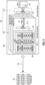
- FIG. 9 illustrates an example operation performed in a memory device according to one or more embodiments.
- the embedding lookup operation may include reading embedding vectors and adding up all the read embedding vectors.
- access to the embedding vectors may be considerably sparse and may randomly occur, and cache utilization may thus decrease.
- embedding vectors 994 to be used for an operation may be stored in a plurality of memory banks, and these memory banks may be distributed to a plurality of memory ranks and distributed furthermore to a plurality of memory channels.
- the memory device 920 may read, from each memory bank, the embedding vectors 994 to be calculated.
- the memory device 920 may calculate a sum of the embedding vectors 994 stored in memory banks through PEs connected in a tree structure within each memory channel.
- a plurality of memory channels may be disposed in a memory core die 922 (e.g., the memory core die 922 may include a plurality of memory core dies).
- a bank-level PE 921-3 may obtain a sum 993 of data (e.g., the embedding vectors 994) between banks.
- a rank-level PE 921-2 may obtain a partial sum (PSUM) 992 (e.g., a partial result) by applying a reduction operation to sums received from memory ranks. Until a partial sum is obtained, an internal bandwidth may be used through PEs in a memory. For example, the partial sum may vary depending on the characteristics of an embedding table or input data.
- the memory device 920 may generate a final operation result 991 by performing an inter-channel operation through a channel-level PE 921-1 disposed in a logic die 921.
- the embedding lookup operation described above may be an operation used in a recommendation system of a graphics processing unit (GPU).
- the memory channels may be connected to a host processor 910.
- the final operation result 991 generated through a reduction operation by the channel-level PE 921-1 of the logic die 921 disposed in the middle may be transmitted to the host processor 910.
- the memory device 920 and/or the electronic device 900 may support an inter-channel operation in PIM.
- the memory device 920 and/or the electronic device 900 of one or more embodiments may effectively accelerate an embedding lookup of a deep learning recommendation model (DLRM) and a sparse matrix multiplication of a graph neural network (GNN), as a memory-centric operation.
- the memory device 920 and/or the electronic device 900 may be applied to accelerate DLRMs or various high-performance computing (HPC) applications using at least one of the embedding lookup or the sparse matrix multiplication.
- the memory device 920 may also be implemented as PIM or PNM.
- the memory device 920 may be provided in a portable device or a server.
- the memory device 920 is not limited to being applied to the deep learning models described above but may be applied to various applications (e.g., the sparse matrix multiplication) having a characteristic of memory bandwidth bottleneck.
- the memory device 920 and/or the electronic device 900 of one or more embodiments may also accelerate a gather-and-reduction operation in such a recommender system.
- the gather-and-reduction operation may include gathering and adding vectors (e.g., embedding vectors) from the embedding table.
- the gather-and-reduction operation which is the most used operation in the recommendation system, may occupy approximately 70% of an operation rate of the DLRM.
- the performance of processing the gather-and-reduction operation may be determined by the speed of reading embedding vectors from the memory device 920.
- the memory device 920 and/or the electronic device 900 of one or more embodiments may accelerate the gather-and-reduction operation by using a tree structure of a memory data path.
- the memory device 920 implemented as PIM may activate a plurality of memory banks, and process data read from the memory banks by PEs formed in the tree structure.
- the memory device 920 of one or more embodiments may thereby maximize the use of internal bandwidth.
- the memory device 920 of one or more embodiments may maximize the use of internal bandwidth by using, for example, three-step parallelism: parallelism between memory banks, parallelism between groups of memory banks, and parallelism between memory ranks.
- an intermediate result value e.g., a partial output
- the host processor 910 may perform an operation (or calculation), which may limit the acceleration.
- the number of memory channels increases, the number of partial outputs may increase, which may cause additional host overhead.
- a spare area may be small on a data path between memory banks or a data path between bank groups, and only PEs supporting limited operations may thus be arranged.
- the memory device 920 and/or the electronic device of one or more embodiments may perform an operation (e.g., a reduction operation) on partial outputs (e.g., partial results) of each memory channel to generate an in-memory computation result (e.g., the final operation result 991).
- the memory device 920 and/or the electronic device of one or more embodiments may provide the final operation result 991, instead of the partial outputs, from the host processor 910 to accelerate an operation.
- 1-9 are implemented by or representative of hardware components.
- hardware components that may be used to perform the operations described in this application where appropriate include controllers, sensors, generators, drivers, memories, comparators, arithmetic logic units, adders, subtractors, multipliers, dividers, integrators, and any other electronic components configured to perform the operations described in this application.
- one or more of the hardware components that perform the operations described in this application are implemented by computing hardware, for example, by one or more processors or computers.
- a processor or computer may be implemented by one or more processing elements, such as an array of logic gates, a controller and an arithmetic logic unit, a digital signal processor, a microcomputer, a programmable logic controller, a field-programmable gate array, a programmable logic array, a microprocessor, or any other device or combination of devices that is configured to respond to and execute instructions in a defined manner to achieve a desired result.
- a processor or computer includes, or is connected to, one or more memories storing instructions or software that are executed by the processor or computer.
- Hardware components implemented by a processor or computer may execute instructions or software, such as an operating system (OS) and one or more software applications that run on the OS, to perform the operations described in this application.
- OS operating system
- the hardware components may also access, manipulate, process, create, and store data in response to execution of the instructions or software.
- processor or “computer” may be used in the description of the examples described in this application, but in other examples multiple processors or computers may be used, or a processor or computer may include multiple processing elements, or multiple types of processing elements, or both.
- a single hardware component or two or more hardware components may be implemented by a single processor, or two or more processors, or a processor and a controller.
- One or more hardware components may be implemented by one or more processors, or a processor and a controller, and one or more other hardware components may be implemented by one or more other processors, or another processor and another controller.
- processors may implement a single hardware component, or two or more hardware components.
- example hardware components may have any one or more of different processing configurations, examples of which include a single processor, independent processors, parallel processors, single-instruction single-data (SISD) multiprocessing, single-instruction multiple-data (SIMD) multiprocessing, multiple-instruction single-data (MISD) multiprocessing, and multiple-instruction multiple-data (MIMD) multiprocessing.
- SISD single-instruction single-data
- SIMD single-instruction multiple-data
- MIMD multiple-instruction multiple-data
- FIGS. 1-9 that perform the operations described in this application are performed by computing hardware, for example, by one or more processors or computers, implemented as described above implementing instructions or software to perform the operations described in this application that are performed by the methods.
- a single operation or two or more operations may be performed by a single processor, or two or more processors, or a processor and a controller.
- One or more operations may be performed by one or more processors, or a processor and a controller, and one or more other operations may be performed by one or more other processors, or another processor and another controller.
- One or more processors, or a processor and a controller may perform a single operation, or two or more operations.
- Instructions or software to control computing hardware may be written as computer programs, code segments, instructions or any combination thereof, for individually or collectively instructing or configuring the one or more processors or computers to operate as a machine or special-purpose computer to perform the operations that are performed by the hardware components and the methods as described above.
- the instructions or software include machine code that is directly executed by the one or more processors or computers, such as machine code produced by a compiler.
- the instructions or software includes higher-level code that is executed by the one or more processors or computer using an interpreter.
- the instructions or software may be written using any programming language based on the block diagrams and the flow charts illustrated in the drawings and the corresponding descriptions herein, which disclose algorithms for performing the operations that are performed by the hardware components and the methods as described above.
- the instructions or software to control computing hardware for example, one or more processors or computers, to implement the hardware components and perform the methods as described above, and any associated data, data files, and data structures, may be recorded, stored, or fixed in or on one or more non-transitory computer-readable storage media, and thus, not a signal per se.
- examples of a non-transitory computer-readable storage medium include one or more of any of read-only memory (ROM), random-access programmable read only memory (PROM), electrically erasable programmable read-only memory (EEPROM), random-access memory (RAM), dynamic random access memory (DRAM), static random access memory (SRAM), flash memory, non-volatile memory, CD-ROMs, CD-Rs, CD+Rs, CD-RWs, CD+RWs, DVD-ROMs, DVD- Rs, DVD+Rs, DVD-RWs, DVD+RWs, DVD-RAMs, BD-ROMs, BD-Rs, BD-R LTHs, BD-REs, blue-ray or optical disk storage, hard disk drive (HDD), solid state drive (SSD), flash memory, a card type memory such as multimedia card micro or a card (for example, secure digital (SD) or extreme digital (XD)), magnetic tapes, floppy disks, magneto
- SD secure digital
- XD extreme
- the instructions or software and any associated data, data files, and data structures are distributed over network-coupled computer systems so that the instructions and software and any associated data, data files, and data structures are stored, accessed, and executed in a distributed fashion by the one or more processors or computers.
Landscapes
- Engineering & Computer Science (AREA)
- Theoretical Computer Science (AREA)
- Physics & Mathematics (AREA)
- General Physics & Mathematics (AREA)
- General Engineering & Computer Science (AREA)
- Computing Systems (AREA)
- Software Systems (AREA)
- Mathematical Analysis (AREA)
- Pure & Applied Mathematics (AREA)
- Computational Mathematics (AREA)
- Computer Hardware Design (AREA)
- Mathematical Optimization (AREA)
- Mathematical Physics (AREA)
- Data Mining & Analysis (AREA)
- Microelectronics & Electronic Packaging (AREA)
- Life Sciences & Earth Sciences (AREA)
- Biophysics (AREA)
- Health & Medical Sciences (AREA)
- Biomedical Technology (AREA)
- Neurology (AREA)
- Human Computer Interaction (AREA)
- Artificial Intelligence (AREA)
- Molecular Biology (AREA)
- Computational Linguistics (AREA)
- Evolutionary Computation (AREA)
- Algebra (AREA)
- Databases & Information Systems (AREA)
- General Health & Medical Sciences (AREA)
- Memory System (AREA)
- Image Processing (AREA)
- Advance Control (AREA)
Applications Claiming Priority (1)
| Application Number | Priority Date | Filing Date | Title |
|---|---|---|---|
| KR1020220166588A KR102850057B1 (ko) | 2022-12-02 | 2022-12-02 | 메모리 장치 및 그 동작 방법 |
Publications (1)
| Publication Number | Publication Date |
|---|---|
| EP4383084A1 true EP4383084A1 (fr) | 2024-06-12 |
Family
ID=88978295
Family Applications (1)
| Application Number | Title | Priority Date | Filing Date |
|---|---|---|---|
| EP23212571.6A Pending EP4383084A1 (fr) | 2022-12-02 | 2023-11-28 | Dispositif de mémoire et son procédé de fonctionnement |
Country Status (4)
| Country | Link |
|---|---|
| US (1) | US20240184526A1 (fr) |
| EP (1) | EP4383084A1 (fr) |
| KR (1) | KR102850057B1 (fr) |
| CN (1) | CN118132470A (fr) |
Families Citing this family (1)
| Publication number | Priority date | Publication date | Assignee | Title |
|---|---|---|---|---|
| US20250208878A1 (en) * | 2023-12-20 | 2025-06-26 | Advanced Micro Devices, Inc. | Accumulation apertures |
Citations (3)
| Publication number | Priority date | Publication date | Assignee | Title |
|---|---|---|---|---|
| US20170337953A1 (en) * | 2015-02-06 | 2017-11-23 | Micron Technology, Inc. | Apparatuses and methods for scatter and gather |
| US20200184001A1 (en) * | 2018-12-07 | 2020-06-11 | Samsung Electronics Co., Ltd. | Dataflow accelerator architecture for general matrix-matrix multiplication and tensor computation in deep learning |
| US20210191871A1 (en) * | 2019-12-20 | 2021-06-24 | Facebook, Inc. | Computer memory module processing device with cache storage |
-
2022
- 2022-12-02 KR KR1020220166588A patent/KR102850057B1/ko active Active
-
2023
- 2023-06-05 US US18/329,045 patent/US20240184526A1/en active Pending
- 2023-11-07 CN CN202311474337.1A patent/CN118132470A/zh active Pending
- 2023-11-28 EP EP23212571.6A patent/EP4383084A1/fr active Pending
Patent Citations (3)
| Publication number | Priority date | Publication date | Assignee | Title |
|---|---|---|---|---|
| US20170337953A1 (en) * | 2015-02-06 | 2017-11-23 | Micron Technology, Inc. | Apparatuses and methods for scatter and gather |
| US20200184001A1 (en) * | 2018-12-07 | 2020-06-11 | Samsung Electronics Co., Ltd. | Dataflow accelerator architecture for general matrix-matrix multiplication and tensor computation in deep learning |
| US20210191871A1 (en) * | 2019-12-20 | 2021-06-24 | Facebook, Inc. | Computer memory module processing device with cache storage |
Also Published As
| Publication number | Publication date |
|---|---|
| US20240184526A1 (en) | 2024-06-06 |
| KR20240083233A (ko) | 2024-06-12 |
| KR102850057B1 (ko) | 2025-08-26 |
| CN118132470A (zh) | 2024-06-04 |
Similar Documents
| Publication | Publication Date | Title |
|---|---|---|
| US11868657B2 (en) | Memory controller, method of operating the memory controller, and electronic device including the memory controller | |
| US9632729B2 (en) | Storage compute device with tiered memory processing | |
| US20240004588A1 (en) | Memory controller and memory control method | |
| US11544213B2 (en) | Neural processor | |
| US12327179B2 (en) | Processor, method of operating the processor, and electronic device including the same | |
| US20240264863A1 (en) | Memory device and method of operating the same | |
| US12314843B2 (en) | Neural network operation method and apparatus with mapping orders | |
| US12223444B2 (en) | Accelerator for processing inference tasks in parallel and operating method thereof | |
| EP3839832A1 (fr) | Procédé et appareil d'opération de convolution de réseau neuronal | |
| CN114118348A (zh) | 加速器、操作加速器的方法以及包括加速器的电子装置 | |
| US20210263870A1 (en) | Accelerator, operation method of the accelerator, and an apparatus including the accelerator | |
| US11797461B2 (en) | Data transmission method for convolution operation, fetcher, and convolution operation apparatus | |
| EP4383084A1 (fr) | Dispositif de mémoire et son procédé de fonctionnement | |
| EP4303739A1 (fr) | Procédé, dispositif et système avec interrogation de hachage basée sur un traitement en mémoire (pim) | |
| US20210397557A1 (en) | Method and apparatus with accelerator processing | |
| US20240111828A1 (en) | In memory computing processor and method thereof with direction-based processing | |
| US11966344B2 (en) | Accelerator and electronic device including the same | |
| US12373677B2 (en) | Neural processor and control method of neural processor | |
| US20240143230A1 (en) | Memory controller and memory control method | |
| US11755898B1 (en) | Near-memory processing of embeddings method and system for reducing memory size and energy in deep learning-based recommendation systems | |
| US12620425B2 (en) | Memory device and method of operating the same | |
| US20240257851A1 (en) | Memory device and method of operating the same | |
| US20250199857A1 (en) | Electronic device and method with tensor management and prefetching | |
| US20230185527A1 (en) | Method and apparatus with data compression | |
| US20260127119A1 (en) | Memory controller for processing in memory and memory generation method using memory controller |
Legal Events
| Date | Code | Title | Description |
|---|---|---|---|
| PUAI | Public reference made under article 153(3) epc to a published international application that has entered the european phase |
Free format text: ORIGINAL CODE: 0009012 |
|
| STAA | Information on the status of an ep patent application or granted ep patent |
Free format text: STATUS: REQUEST FOR EXAMINATION WAS MADE |
|
| 17P | Request for examination filed |
Effective date: 20231128 |
|
| AK | Designated contracting states |
Kind code of ref document: A1 Designated state(s): AL AT BE BG CH CY CZ DE DK EE ES FI FR GB GR HR HU IE IS IT LI LT LU LV MC ME MK MT NL NO PL PT RO RS SE SI SK SM TR |