EP4383241A1 - Appareil d'affichage et son procédé de commande - Google Patents
Appareil d'affichage et son procédé de commande Download PDFInfo
- Publication number
- EP4383241A1 EP4383241A1 EP23214486.5A EP23214486A EP4383241A1 EP 4383241 A1 EP4383241 A1 EP 4383241A1 EP 23214486 A EP23214486 A EP 23214486A EP 4383241 A1 EP4383241 A1 EP 4383241A1
- Authority
- EP
- European Patent Office
- Prior art keywords
- image signal
- pixels
- shift time
- coordinate information
- display apparatus
- Prior art date
- Legal status (The legal status is an assumption and is not a legal conclusion. Google has not performed a legal analysis and makes no representation as to the accuracy of the status listed.)
- Pending
Links
Images





Classifications
-
- G—PHYSICS
- G09—EDUCATION; CRYPTOGRAPHY; DISPLAY; ADVERTISING; SEALS
- G09G—ARRANGEMENTS OR CIRCUITS FOR CONTROL OF INDICATING DEVICES USING STATIC MEANS TO PRESENT VARIABLE INFORMATION
- G09G3/00—Control arrangements or circuits, of interest only in connection with visual indicators other than cathode-ray tubes
- G09G3/20—Control arrangements or circuits, of interest only in connection with visual indicators other than cathode-ray tubes for presentation of an assembly of a number of characters, e.g. a page, by composing the assembly by combination of individual elements arranged in a matrix no fixed position being assigned to or needed to be assigned to the individual characters or partial characters
- G09G3/2092—Details of a display terminals using a flat panel, the details relating to the control arrangement of the display terminal and to the interfaces thereto
- G09G3/2096—Details of the interface to the display terminal specific for a flat panel
-
- G—PHYSICS
- G09—EDUCATION; CRYPTOGRAPHY; DISPLAY; ADVERTISING; SEALS
- G09G—ARRANGEMENTS OR CIRCUITS FOR CONTROL OF INDICATING DEVICES USING STATIC MEANS TO PRESENT VARIABLE INFORMATION
- G09G5/00—Control arrangements or circuits for visual indicators common to cathode-ray tube indicators and other visual indicators
- G09G5/36—Control arrangements or circuits for visual indicators common to cathode-ray tube indicators and other visual indicators characterised by the display of a graphic pattern, e.g. using an all-points-addressable [APA] memory
- G09G5/38—Control arrangements or circuits for visual indicators common to cathode-ray tube indicators and other visual indicators characterised by the display of a graphic pattern, e.g. using an all-points-addressable [APA] memory with means for controlling the display position
-
- G—PHYSICS
- G09—EDUCATION; CRYPTOGRAPHY; DISPLAY; ADVERTISING; SEALS
- G09G—ARRANGEMENTS OR CIRCUITS FOR CONTROL OF INDICATING DEVICES USING STATIC MEANS TO PRESENT VARIABLE INFORMATION
- G09G3/00—Control arrangements or circuits, of interest only in connection with visual indicators other than cathode-ray tubes
- G09G3/007—Use of pixel shift techniques, e.g. by mechanical shift of the physical pixels or by optical shift of the perceived pixels
-
- G—PHYSICS
- G09—EDUCATION; CRYPTOGRAPHY; DISPLAY; ADVERTISING; SEALS
- G09G—ARRANGEMENTS OR CIRCUITS FOR CONTROL OF INDICATING DEVICES USING STATIC MEANS TO PRESENT VARIABLE INFORMATION
- G09G3/00—Control arrangements or circuits, of interest only in connection with visual indicators other than cathode-ray tubes
- G09G3/20—Control arrangements or circuits, of interest only in connection with visual indicators other than cathode-ray tubes for presentation of an assembly of a number of characters, e.g. a page, by composing the assembly by combination of individual elements arranged in a matrix no fixed position being assigned to or needed to be assigned to the individual characters or partial characters
-
- G—PHYSICS
- G09—EDUCATION; CRYPTOGRAPHY; DISPLAY; ADVERTISING; SEALS
- G09G—ARRANGEMENTS OR CIRCUITS FOR CONTROL OF INDICATING DEVICES USING STATIC MEANS TO PRESENT VARIABLE INFORMATION
- G09G3/00—Control arrangements or circuits, of interest only in connection with visual indicators other than cathode-ray tubes
- G09G3/20—Control arrangements or circuits, of interest only in connection with visual indicators other than cathode-ray tubes for presentation of an assembly of a number of characters, e.g. a page, by composing the assembly by combination of individual elements arranged in a matrix no fixed position being assigned to or needed to be assigned to the individual characters or partial characters
- G09G3/34—Control arrangements or circuits, of interest only in connection with visual indicators other than cathode-ray tubes for presentation of an assembly of a number of characters, e.g. a page, by composing the assembly by combination of individual elements arranged in a matrix no fixed position being assigned to or needed to be assigned to the individual characters or partial characters by control of light from an independent source
- G09G3/36—Control arrangements or circuits, of interest only in connection with visual indicators other than cathode-ray tubes for presentation of an assembly of a number of characters, e.g. a page, by composing the assembly by combination of individual elements arranged in a matrix no fixed position being assigned to or needed to be assigned to the individual characters or partial characters by control of light from an independent source using liquid crystals
- G09G3/3607—Control arrangements or circuits, of interest only in connection with visual indicators other than cathode-ray tubes for presentation of an assembly of a number of characters, e.g. a page, by composing the assembly by combination of individual elements arranged in a matrix no fixed position being assigned to or needed to be assigned to the individual characters or partial characters by control of light from an independent source using liquid crystals for displaying colours or for displaying grey scales with a specific pixel layout, e.g. using sub-pixels
-
- G—PHYSICS
- G09—EDUCATION; CRYPTOGRAPHY; DISPLAY; ADVERTISING; SEALS
- G09G—ARRANGEMENTS OR CIRCUITS FOR CONTROL OF INDICATING DEVICES USING STATIC MEANS TO PRESENT VARIABLE INFORMATION
- G09G2310/00—Command of the display device
- G09G2310/08—Details of timing specific for flat panels, other than clock recovery
-
- G—PHYSICS
- G09—EDUCATION; CRYPTOGRAPHY; DISPLAY; ADVERTISING; SEALS
- G09G—ARRANGEMENTS OR CIRCUITS FOR CONTROL OF INDICATING DEVICES USING STATIC MEANS TO PRESENT VARIABLE INFORMATION
- G09G2320/00—Control of display operating conditions
- G09G2320/02—Improving the quality of display appearance
- G09G2320/0257—Reduction of after-image effects
-
- G—PHYSICS
- G09—EDUCATION; CRYPTOGRAPHY; DISPLAY; ADVERTISING; SEALS
- G09G—ARRANGEMENTS OR CIRCUITS FOR CONTROL OF INDICATING DEVICES USING STATIC MEANS TO PRESENT VARIABLE INFORMATION
- G09G2320/00—Control of display operating conditions
- G09G2320/04—Maintaining the quality of display appearance
- G09G2320/043—Preventing or counteracting the effects of ageing
- G09G2320/046—Dealing with screen burn-in prevention or compensation of the effects thereof
-
- G—PHYSICS
- G09—EDUCATION; CRYPTOGRAPHY; DISPLAY; ADVERTISING; SEALS
- G09G—ARRANGEMENTS OR CIRCUITS FOR CONTROL OF INDICATING DEVICES USING STATIC MEANS TO PRESENT VARIABLE INFORMATION
- G09G2320/00—Control of display operating conditions
- G09G2320/06—Adjustment of display parameters
- G09G2320/0626—Adjustment of display parameters for control of overall brightness
-
- G—PHYSICS
- G09—EDUCATION; CRYPTOGRAPHY; DISPLAY; ADVERTISING; SEALS
- G09G—ARRANGEMENTS OR CIRCUITS FOR CONTROL OF INDICATING DEVICES USING STATIC MEANS TO PRESENT VARIABLE INFORMATION
- G09G2340/00—Aspects of display data processing
- G09G2340/04—Changes in size, position or resolution of an image
- G09G2340/0464—Positioning
-
- G—PHYSICS
- G09—EDUCATION; CRYPTOGRAPHY; DISPLAY; ADVERTISING; SEALS
- G09G—ARRANGEMENTS OR CIRCUITS FOR CONTROL OF INDICATING DEVICES USING STATIC MEANS TO PRESENT VARIABLE INFORMATION
- G09G2340/00—Aspects of display data processing
- G09G2340/04—Changes in size, position or resolution of an image
- G09G2340/0464—Positioning
- G09G2340/0471—Vertical positioning
-
- G—PHYSICS
- G09—EDUCATION; CRYPTOGRAPHY; DISPLAY; ADVERTISING; SEALS
- G09G—ARRANGEMENTS OR CIRCUITS FOR CONTROL OF INDICATING DEVICES USING STATIC MEANS TO PRESENT VARIABLE INFORMATION
- G09G2340/00—Aspects of display data processing
- G09G2340/04—Changes in size, position or resolution of an image
- G09G2340/0464—Positioning
- G09G2340/0478—Horizontal positioning
-
- G—PHYSICS
- G09—EDUCATION; CRYPTOGRAPHY; DISPLAY; ADVERTISING; SEALS
- G09G—ARRANGEMENTS OR CIRCUITS FOR CONTROL OF INDICATING DEVICES USING STATIC MEANS TO PRESENT VARIABLE INFORMATION
- G09G2340/00—Aspects of display data processing
- G09G2340/16—Determination of a pixel data signal depending on the signal applied in the previous frame
-
- G—PHYSICS
- G09—EDUCATION; CRYPTOGRAPHY; DISPLAY; ADVERTISING; SEALS
- G09G—ARRANGEMENTS OR CIRCUITS FOR CONTROL OF INDICATING DEVICES USING STATIC MEANS TO PRESENT VARIABLE INFORMATION
- G09G2360/00—Aspects of the architecture of display systems
- G09G2360/16—Calculation or use of calculated indices related to luminance levels in display data
Definitions
- Embodiments of the present disclosure relate to a display apparatus.
- the display apparatus include a liquid crystal display (LCD), an organic light-emitting diode (OLED) display, a mini light-emitting diode (mini LED) display, a micro light-emitting diode (micro LED) display, and a quantum dot light-emitting diode (QLED) display.
- LCD liquid crystal display
- OLED organic light-emitting diode
- mini LED mini LED
- QLED quantum dot light-emitting diode
- the present invention is not limited to any particular apparatus.
- the display apparatus referred to herein may be, for example, a finished product itself (e.g., TV, digital signage, cell phone, car navigation, etc.) or a component (e.g., driver IC, T-CON, etc.) that controls the display module.
- burn-in For example, if the same image is left on the display apparatus, or the image of a broadcaster whose position is fixed on each channel is continuously exposed on the screen, the color cannot be represented properly on the corresponding part or a residual image (smudge) is left on the screen, which is called burn-in.
- the aforementioned burn-in phenomenon may cause problems in a variety of display apparatuses.
- the following discussion will focus on OLEDs as an example.
- OLED display apparatuses are made up of organic materials. OLEDs are vulnerable to light and heat, and their brightness and color reproduction decrease with increasing use.
- the conventional technology attempts to reduce degradation by scaling (zooming in or out) the image signal to move a fixed image.
- the amount of pixel movement is adjusted depending on whether the image signal is a still image or a rapidly changing moving image.
- the amount of pixel movement increases when the image is a still image, and thus may be easily perceived by the user's eyes.
- One of the embodiments of the present disclosure is intended to prevent degradation by shifting a fixed image by shifting the entire image signal.
- One of the embodiments of the present disclosure provides a novel system that reduces the likelihood of a user perceiving a change and eliminates the need for a separate scaler by adjusting the period (time) of pixel shift, rather than adjusting the amount of pixel shift.
- a display apparatus may include an interface configured to receive an image signal, a memory having track coordinate information stored therein, a first calculator configured to calculate a complexity of the received image signal, a second calculator configured to calculate an average picture level (APL) of the received image signal, and a controller configured to determine a final shift time of pixels based on the calculated complexity and APL of the image signal and to control the received image signal to be shifted in a horizontal direction or a vertical direction based on the track coordinate information stored in the memory and the determined final shift time of the pixels.
- APL average picture level
- the complexity of the received image signal may be inversely proportional to the final shift time of the pixels, whereas the APL of the received image signal may be proportional to the final shift time of the pixels.
- the controller may determine the final shift time as a product of a default time, a first gain of a shift time according to the calculated complexity of the image signal, and a second gain of a shift time according to the calculated APL of the image signal.
- the first gain and the second gain may be, for example, in a range of 0 to 1.
- a plurality of sets of the track coordinate information may be stored in the memory, wherein a set of the track coordinate information may be randomly selected from among the sets of track coordinate information after an end of the final shift time of the pixels.
- the shift of the image signal in the horizontal may be limited to a maximum of 10 pixels, and the shift of the image signal in the vertical direction may be limited to a maximum of 5 pixels.
- a method for controlling a display apparatus may include receiving an image signal, calculating at least one of a complexity or an average picture level (APL) of the received image signal, determining a final shift time of pixels based on the at least one of the calculated complexity or APL of the image signal, and shifting the received image signal in a horizontal direction or a vertical direction and outputting the shifted image signal, based on track coordinate information stored in a memory and the determined final shift time of the pixels.
- APL average picture level
- a third party to implement a computer-readable medium (e.g., application, memory, software, etc.) having recorded thereon a program that performs any of the above-described methods and various embodiments described herein.
- a computer-readable medium e.g., application, memory, software, etc.
- a novel system that reduces the likelihood of a user perceiving a change and eliminates the need for a separate scaler by adjusting the period (time) of pixel shift, rather than adjusting the amount of pixel shift may be provided.
- first and second may be used to describe various components, but the components are not limited by such terms. These terms are used only to distinguish one component from another. When a component is described as being “connected” or “linked” to another component, it should be understood that it may be directly connected or linked to the other component, but there may be other components in between.
- FIG. 1 is a diagram illustrating a configuration of a display apparatus according to one embodiment of the present disclosure.
- a display apparatus 100 includes a display panel 110, a display driver 120, a data driver 140, and a gate driver 150.
- a display driver 120 includes a display driver 120, a data driver 140, and a gate driver 150.
- some modules may be added, removed, or changed according to the needs of those skilled in the art.
- the display panel 110 includes a plurality of gate lines GL 1-GLn and a plurality of data lines DL1-DLm that are arranged crosswise to each other to define a plurality of pixel regions, and pixels P provided in each of the plurality of pixel regions.
- the plurality of gate lines GL1-GLn may be arranged in a horizontal direction and the plurality of data lines DL1-DLm may be arranged in a vertical direction.
- embodiments are not necessarily limited thereto.
- the display panel 110 may be a liquid crystal display (LCD) panel.
- the display panel 110 is an LCD panel, the display panel 110 includes thin-film transistors (TFTs) formed in the pixel regions P defined by the plurality of gate lines GL1-GLn and the plurality of data lines DL1-DLm, and liquid crystal cells connected to the TFTs.
- TFTs thin-film transistors
- the present disclosure is applicable not only to LCDs, but also to micro LEDs, mini LEDs, OLEDs, and the like.
- the TFTs supply data signals supplied through the data lines DL1-DLm to the liquid crystal cells in response to scan pulses supplied through the gate lines GL1-GLn.
- the liquid crystal cell includes a common electrode and a sub-pixel electrode facing each other across the liquid crystal, the subpixel electrode being connected to a TFT.
- a liquid crystal capacitor Clc Such a liquid crystal cell includes a storage capacitor Cst connected to the previous gate line to maintain the data signal charged in the liquid crystal capacitor Clc until the next data signal is charged.
- a pixel region of the display panel 110 may include red (R), green (G), and blue (B) subpixels.
- the subpixels may be repeatedly arranged in order of R, G, and B within one horizontal line.
- two subpixels connected to the same data line may be configured as subpixels of different colors.
- the first horizontal line may set the last subpixel as a dummy pixel
- the second horizontal line adjacent to the first horizontal line may set the first subpixel as a dummy pixel, such that two subpixels of different colors in the first and second horizontal lines may be connected to the same data line.
- the display panel 110 has been described as an LCD panel in the above-described embodiment, the display panel 110 may be an organic light emitting diode (OLED) panel in which three-color subpixels are formed in each pixel region.
- OLED organic light emitting diode
- the display panel 110 has been described as having three-color subpixels in the embodiment described above, the display panel 110 may have red (R), green (G), blue (B), and white (W) subpixels in other embodiments.
- the display driver 120 is configured to drive the display panel, and includes a timing controller 122 and an overdriving controller 124.
- the timing controller 122 receives various timing signals, including a vertical synchronization signal Vsync, a horizontal synchronization signal Hsync, a data enable (DE) signal, and a clock signal CLK, from an external system (not shown) and generates a data control signal (DCS) to control the data driver 140 and a gate control signal (GCS) to control the gate driver 150.
- Vsync vertical synchronization signal
- Hsync horizontal synchronization signal
- CLK clock signal
- the DCS may include a source start pulse (SSP), a source sampling clock (SSC), and a source output enable signal
- the GCS may include a gate start pulse (GSP), a gate shift clock (GSC), and a gate output enable signal.
- the SSP controls the timing of the start of data sampling of one or more source driver integrated circuits (ICs) constituting the data driver 140.
- the SSC is a clock signal that controls the sampling timing of data in each of the source driver ICs.
- the source output enable signal controls the output timing of the data driver 140.
- the GSP controls the timing of the start of operation of one or more gate driver ICs that constitute the gate driver 150.
- the GSC which is a clock signal input to the one or more gate driver ICs in common, controls the shift timing of the scan signal (gate pulse).
- the gate output enable signal specifies the timing information about the one or more gate driver ICs.
- the timing controller 122 forwards image data Idata received from an external system (not shown) to the overdriving controller 124.
- the timing controller 122 receives pixel data (Idata) corresponding to the image data or overdrive pixel data Idata' from the overdriving controller 124, converts the same into a data signal processable by the data driver 140, and outputs the data signal to the data driver 140.
- the overdriving controller 124 determines whether the current subpixel is overdriven by comparing the current subpixel with a previous subpixel on a per horizontal line basis in the image data. When the overdriving controller 124 determines that the current subpixel is overdriven, it generates overdriven pixel data about the current subpixel.
- FIG. 2 ( a) and FIG. 2(b) illustrate[[s]] a result output by a display apparatus of one embodiment of the present disclosure by shifting a still image or the like.
- the entire image signal 110 is shifted to mitigate the degradation as the fixed image is shifted.
- the portion of the image signal that is shifted out of the screen is deleted, and the blank area 111 is output in black.
- the amount of pixel shifting is not adjusted, but the period (time) of pixel shifting is adjusted.
- the amount of pixel shifting is fixed to, for example, one pixel at a time, while the period (time) of pixel shifting is designed to be automatically adjustable.
- the period (time) of pixel shifting may be adjusted according to the complexity of the image signal.
- the complexity of the image signal is high, there are many edges, and thus the degradation is highly likely to increase. Therefore, in this case, it is important to reduce the time interval between pixel shifts.
- the path along which the pixels are shifted may be named a track.
- the track may be input (edited) through an external interface such as i2c (Inter-Integrated Circuit).
- FIG. 3 illustrates an exemplary track along which a display apparatus according to one embodiment of the present disclosure shifts a still image or the like.
- the entire image is shifted up, down, left, and right by one pixel at a time to mitigate the degradation caused by a fixed image.
- it is important that the shifting is performed as slowly as possible (e.g., within 180 seconds or 120 seconds) so as to be unrecognizable to the user.
- the entire image is shifted by one pixel with respect to the center point (0,0) 200 along the paths (1), (2), (3), (4), (5), (6), (7), and (8).
- the present disclosure is not necessarily limited to the numerical values described below. It is also within the scope of the present disclosure to limit the shift to a maximum of +/- 10 pixels in the horizontal direction H, and to limit the shift to a maximum of +/- 5 pixels in the vertical direction V, as shown in FIG. 3 .
- FIG. 4 is a block diagram illustrating components of a display apparatus according to one embodiment of the present disclosure.
- a display apparatus includes a line memory 310, a complexity calculator 320, an APL calculator 330, a time computation unit 340, and a coordinate memory 350.
- a line memory 310 includes a line memory 310, a complexity calculator 320, an APL calculator 330, a time computation unit 340, and a coordinate memory 350.
- the line memory 310 serves as a buffer to store a received image signal for a certain time.
- the image signal may be received from a module outside or inside the display apparatus via an interface (not shown).
- the coordinate memory 350 stores track coordinate information.
- the track coordinate information will be described in more detail below with reference to FIG. 8 and the like.
- the complexity calculator 320 calculates the complexity of the received image signal. This calculator may be referred to as a first calculator.
- the APL calculator 330 calculates the APL of the received image signal. This calculator may be referred to as a second calculator.
- the time computation unit 340 determines the final shifting time of pixels based on the calculated complexity and APL of the image signal.
- the received image signal is shifted in the vertical direction unit (360) and is shifted in the horizontal direction unit (370).
- a controller in the present disclosure.
- FIG. 5 is a flowchart illustrating a method for controlling a display apparatus according to one embodiment of the present disclosure.
- the display apparatus determines whether an image signal is received (operation S301).
- the display apparatus determines whether to use the complexity of the image signal (operation S302).
- a final shift time of pixels is determined based on at least one of the complexity of the image signal calculated in operation S303 or the APL of the image signal calculated in operation S305 (operation S306). Related details will be described below with reference to FIGS. 7 and 8 .
- the display apparatus determines whether to use a fixed coordinate set (operation S307).
- the received image signal is designed to be shifted in the vertical direction and output (operation S310) and to be shifted in the horizontal direction and output (operation S311).
- the display apparatus receives an image signal.
- the display apparatus calculates at least one of a complexity or APL of the received image signal.
- the display apparatus determines a final shift time of pixels based on at least one of the calculated complexity or APL of the image signal.
- the display apparatus may shift the received image signal in a horizontal direction or a vertical direction and output the same, thereby mitigating the degradation of image quality.
- Operation S303 will be described in more detail below with reference to FIG. 5
- operation S305 will be described in more detail below with reference to FIG. 7 .
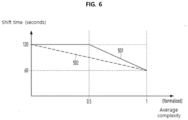
- FIG. 6 is a graph illustrating determining, by a display apparatus according to one embodiment of the present disclosure, a pixel shift time based on a complexity of an image signal.
- the complexity of the image signal may be calculated by adding up all the values obtained through an edge detection filter (e.g., Sobel filter). As the value obtained through the edge detection filter increases, the complexity of the image signal is considered to be higher.
- an edge detection filter e.g., Sobel filter
- the final shift time of pixels is set to a shorter time. This is because higher complexity means that the image has more edges, which can be better perceived by the user's eyes when degraded.
- the complexity of an image signal may be determined based on the average complexity of multiple frames. For example, taking the average complexity of the last 120 frames is also within the scope of the present disclosure.
- the first embodiment 501 represents a case where the image complexity is maintained and then decreased over the shift time
- the second embodiment 502 represents a case where the image complexity is decreased from the beginning.
- the final shift time of the pixels starts to decrease only when the complexity of the image signal exceeds a preset value (0.5).
- the final shift time of the pixels is designed to decrease proportionally regardless of whether the complexity of the image signal reaches the preset value (0.5).
- FIG. 7 is a graph illustrating determining, by a display apparatus according to one embodiment of the present disclosure, a pixel shift time based on an APL.
- the average of the Y-values of all pixels may be used as the value of the APL.
- (R+G+B)/3 may be used instead of the Y-value.
- R corresponds to data for a red pixel
- G corresponds to data for a green pixel
- B corresponds to data for a blue pixel
- Y corresponds to luminance data.
- the shift time of the pixels is adjusted according to the value of the APL obtained above. As the APL decreases, the shift time of the pixels is set to be shorter.
- the design takes into account that a low APL increases the peak luminance, and in this case, the pixels in a small region emit high luminance, which leads to severe degradation.
- the APL of an image signal may be based on the average of multiple frames. For example, using an average of the APLs of the last 120 frames is also within the scope of the present disclosure.
- the second embodiment 602 represents a case where the APL is maintained and then increased over the shift time, while the first embodiment 601 represents a case where the APL is increased from the beginning.
- the final shift time of the pixels starts to increase only when the APL of the image signal exceeds a preset value (0.25).
- the final shift time of the pixels is designed to increase proportionally regardless of whether the APL of the image signal reaches the preset value (0.25).
- Both the first embodiment 601 and the second embodiment 602 illustrated in FIG. 7 fall within the scope of the present disclosure.
- the gain of the shift time of the pixel according to the complexity of the image signal and the APL may be normalized to 0 to 1.
- the gain of the shift time according to the complexity of the image signal is defined as a first gain, and the gain of the shift time according to the APL of the image signal is defined as a second gain.
- At least one of the first gain or the second gain can be used.
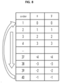
- FIG. 8 illustrates an exemplary table of track coordinate information about a pixel used by a display apparatus according to one embodiment of the present disclosure.
- FIG. 9 (a) and FIG. 9(b) illustrate[[s]] a process in which a position of an image signal is changed and output based on the table shown in FIG. 8 .
- track coordinate information about pixels is stored in the memory, for example, in a table format.
- Table 1 below is an exemplary table, showing in more detail FIG. 7 , which shows the shift track of the pixels around the center point (0, 0).
- the shift is designed to be no more than +/- 10 pixels along the X axis and no more than +/- 5 pixels along the Y axis.
- the entire image changes along the path of shift, and the blank space created by the change in pixel position is designed to be processed in black.
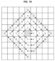
- FIG. 10 sequentially illustrates an example of a path along which a display apparatus according to one embodiment of the present disclosure changes a position of an image signal.
- FIG. 11 sequentially illustrates another example of a path along which a display apparatus according to one embodiment of the present disclosure changes a position of an image signal.
- the track shape that serves as the basis for the path along which pixels are shifted may be configured in various ways. Multiple track coordinate sets may be stored a nd any one of them may be selected and used.
- the pixels may be repositioned to the same particular track coordinate set ( FIG. 8 ).
- the examples of the present disclosure may be embodied as computer readable code on a medium on which a program is recorded.
- the computer readable medium includes all kinds of recording devices capable of storing data readable by a computer system is stored. Examples of computer-readable media include applications, hard disk drives (HDDs), solid state disks (SSDs), silicon disk drives (SDDs), ROMs, RAMs, CD-ROMs, magnetic tapes, floppy disks, and optical data storage devices, and also include those implemented in the form of carrier waves (e.g., transmission over the Internet).
Landscapes
- Engineering & Computer Science (AREA)
- Physics & Mathematics (AREA)
- Computer Hardware Design (AREA)
- General Physics & Mathematics (AREA)
- Theoretical Computer Science (AREA)
- Chemical & Material Sciences (AREA)
- Crystallography & Structural Chemistry (AREA)
- Control Of Indicators Other Than Cathode Ray Tubes (AREA)
- Control Of El Displays (AREA)
Applications Claiming Priority (2)
| Application Number | Priority Date | Filing Date | Title |
|---|---|---|---|
| KR20220169612 | 2022-12-07 | ||
| KR1020230142892A KR20240085154A (ko) | 2022-12-07 | 2023-10-24 | 디스플레이 장치 및 그 제어 방법 |
Publications (1)
| Publication Number | Publication Date |
|---|---|
| EP4383241A1 true EP4383241A1 (fr) | 2024-06-12 |
Family
ID=89121656
Family Applications (1)
| Application Number | Title | Priority Date | Filing Date |
|---|---|---|---|
| EP23214486.5A Pending EP4383241A1 (fr) | 2022-12-07 | 2023-12-06 | Appareil d'affichage et son procédé de commande |
Country Status (3)
| Country | Link |
|---|---|
| US (1) | US12249267B2 (fr) |
| EP (1) | EP4383241A1 (fr) |
| TW (1) | TW202424700A (fr) |
Families Citing this family (1)
| Publication number | Priority date | Publication date | Assignee | Title |
|---|---|---|---|---|
| US20250265975A1 (en) * | 2024-02-19 | 2025-08-21 | Lg Display Co., Ltd. | Data driving circuit and display device |
Citations (3)
| Publication number | Priority date | Publication date | Assignee | Title |
|---|---|---|---|---|
| US20190156726A1 (en) * | 2017-11-21 | 2019-05-23 | Lg Electronics Inc. | Organic light emitting diode display device and method for operating thereof |
| KR20220169612A (ko) | 2021-06-21 | 2022-12-28 | 삼익정공(주) | 다각형 가이드 구조체 및 이를 이용한 다기능 액추에이터 |
| KR20230142892A (ko) | 2022-04-04 | 2023-10-11 | 서울대학교병원 | 방광 상태를 측정하기 위한 장치 및 방법 |
Family Cites Families (1)
| Publication number | Priority date | Publication date | Assignee | Title |
|---|---|---|---|---|
| JP6365153B2 (ja) * | 2014-09-10 | 2018-08-01 | 株式会社ソシオネクスト | 画像符号化方法および画像符号化装置 |
-
2023
- 2023-12-06 TW TW112147468A patent/TW202424700A/zh unknown
- 2023-12-06 EP EP23214486.5A patent/EP4383241A1/fr active Pending
- 2023-12-07 US US18/532,216 patent/US12249267B2/en active Active
Patent Citations (3)
| Publication number | Priority date | Publication date | Assignee | Title |
|---|---|---|---|---|
| US20190156726A1 (en) * | 2017-11-21 | 2019-05-23 | Lg Electronics Inc. | Organic light emitting diode display device and method for operating thereof |
| KR20220169612A (ko) | 2021-06-21 | 2022-12-28 | 삼익정공(주) | 다각형 가이드 구조체 및 이를 이용한 다기능 액추에이터 |
| KR20230142892A (ko) | 2022-04-04 | 2023-10-11 | 서울대학교병원 | 방광 상태를 측정하기 위한 장치 및 방법 |
Also Published As
| Publication number | Publication date |
|---|---|
| US20240194118A1 (en) | 2024-06-13 |
| TW202424700A (zh) | 2024-06-16 |
| US12249267B2 (en) | 2025-03-11 |
Similar Documents
| Publication | Publication Date | Title |
|---|---|---|
| KR102819291B1 (ko) | 디스플레이 구동 회로, 이를 포함하는 디스플레이 장치 및 디스플레이 구동 회로의 동작 방법 | |
| CN113450711B (zh) | 显示装置及其驱动方法,驱动装置 | |
| KR102676310B1 (ko) | 표시 패널 구동 방법 | |
| US9691353B2 (en) | Display device and method of adjusting luminance of a logo region of an image displayed on the same | |
| US10157568B2 (en) | Image processing method, image processing circuit, and organic light emitting diode display device using the same | |
| KR102652237B1 (ko) | 표시 장치 및 이의 구동 방법 | |
| US10885831B2 (en) | Display method and display system of singular-shaped display panel, storage device and display device | |
| US11069312B2 (en) | Electronic device, display device and display control method | |
| KR102581719B1 (ko) | 얼룩 특성에 기초하여 휘도 보상 데이터를 생성하기 위한 장치 및 방법 및 휘도 보상을 수행하기 위한 장치 및 방법 | |
| US9779514B2 (en) | Display device, display panel driver and driving method of display panel | |
| KR101274707B1 (ko) | 표시 결함을 보상하기 위한 영상 표시 장치의 보상 회로 및방법 | |
| US20080246784A1 (en) | Display device | |
| US20190206337A1 (en) | Display apparatus and control method thereof | |
| US8350793B2 (en) | Image over-driving devices and image over-driving controlling methods | |
| CN101281716B (zh) | 显示装置 | |
| US20110254850A1 (en) | Image processing apparatus, display system, electronic apparatus and method of processing image | |
| KR20160046983A (ko) | 소비 전력 제어 방법 및 장치와 이를 이용한 표시장치 | |
| EP4383241A1 (fr) | Appareil d'affichage et son procédé de commande | |
| KR102575261B1 (ko) | 주위조도에 따라 영상의 밝기를 조절하는 디스플레이 구동장치 및 구동방법 | |
| TWI416476B (zh) | 液晶裝置、其控制電路及電子機器 | |
| TWI408661B (zh) | 液晶顯示裝置及其驅動方法 | |
| JP2022172980A (ja) | 表示制御装置、電子機器、制御プログラムおよび表示制御方法 | |
| KR20240085154A (ko) | 디스플레이 장치 및 그 제어 방법 | |
| CN118158372A (zh) | 显示设备及其控制方法 | |
| CN117355891A (zh) | 有源矩阵显示器中的选择性黑电平控制 |
Legal Events
| Date | Code | Title | Description |
|---|---|---|---|
| PUAI | Public reference made under article 153(3) epc to a published international application that has entered the european phase |
Free format text: ORIGINAL CODE: 0009012 |
|
| STAA | Information on the status of an ep patent application or granted ep patent |
Free format text: STATUS: THE APPLICATION HAS BEEN PUBLISHED |
|
| AK | Designated contracting states |
Kind code of ref document: A1 Designated state(s): AL AT BE BG CH CY CZ DE DK EE ES FI FR GB GR HR HU IE IS IT LI LT LU LV MC ME MK MT NL NO PL PT RO RS SE SI SK SM TR |
|
| STAA | Information on the status of an ep patent application or granted ep patent |
Free format text: STATUS: REQUEST FOR EXAMINATION WAS MADE |
|
| 17P | Request for examination filed |
Effective date: 20241211 |
|
| STAA | Information on the status of an ep patent application or granted ep patent |
Free format text: STATUS: EXAMINATION IS IN PROGRESS |
|
| 17Q | First examination report despatched |
Effective date: 20260320 |