EP4383351A1 - Cellule solaire, son procédé de préparation et module photovoltaïque - Google Patents
Cellule solaire, son procédé de préparation et module photovoltaïque Download PDFInfo
- Publication number
- EP4383351A1 EP4383351A1 EP23167462.3A EP23167462A EP4383351A1 EP 4383351 A1 EP4383351 A1 EP 4383351A1 EP 23167462 A EP23167462 A EP 23167462A EP 4383351 A1 EP4383351 A1 EP 4383351A1
- Authority
- EP
- European Patent Office
- Prior art keywords
- region
- doped
- layer
- substrate
- metal pattern
- Prior art date
- Legal status (The legal status is an assumption and is not a legal conclusion. Google has not performed a legal analysis and makes no representation as to the accuracy of the status listed.)
- Granted
Links
Images


Classifications
-
- H—ELECTRICITY
- H10—SEMICONDUCTOR DEVICES; ELECTRIC SOLID-STATE DEVICES NOT OTHERWISE PROVIDED FOR
- H10F—INORGANIC SEMICONDUCTOR DEVICES SENSITIVE TO INFRARED RADIATION, LIGHT, ELECTROMAGNETIC RADIATION OF SHORTER WAVELENGTH OR CORPUSCULAR RADIATION
- H10F10/00—Individual photovoltaic cells, e.g. solar cells
- H10F10/10—Individual photovoltaic cells, e.g. solar cells having potential barriers
- H10F10/14—Photovoltaic cells having only PN homojunction potential barriers
-
- H—ELECTRICITY
- H10—SEMICONDUCTOR DEVICES; ELECTRIC SOLID-STATE DEVICES NOT OTHERWISE PROVIDED FOR
- H10F—INORGANIC SEMICONDUCTOR DEVICES SENSITIVE TO INFRARED RADIATION, LIGHT, ELECTROMAGNETIC RADIATION OF SHORTER WAVELENGTH OR CORPUSCULAR RADIATION
- H10F10/00—Individual photovoltaic cells, e.g. solar cells
- H10F10/10—Individual photovoltaic cells, e.g. solar cells having potential barriers
- H10F10/16—Photovoltaic cells having only PN heterojunction potential barriers
- H10F10/163—Photovoltaic cells having only PN heterojunction potential barriers comprising only Group III-V materials, e.g. GaAs/AlGaAs or InP/GaInAs photovoltaic cells
-
- H—ELECTRICITY
- H10—SEMICONDUCTOR DEVICES; ELECTRIC SOLID-STATE DEVICES NOT OTHERWISE PROVIDED FOR
- H10F—INORGANIC SEMICONDUCTOR DEVICES SENSITIVE TO INFRARED RADIATION, LIGHT, ELECTROMAGNETIC RADIATION OF SHORTER WAVELENGTH OR CORPUSCULAR RADIATION
- H10F10/00—Individual photovoltaic cells, e.g. solar cells
- H10F10/10—Individual photovoltaic cells, e.g. solar cells having potential barriers
- H10F10/16—Photovoltaic cells having only PN heterojunction potential barriers
- H10F10/164—Photovoltaic cells having only PN heterojunction potential barriers comprising heterojunctions with Group IV materials, e.g. ITO/Si or GaAs/SiGe photovoltaic cells
- H10F10/165—Photovoltaic cells having only PN heterojunction potential barriers comprising heterojunctions with Group IV materials, e.g. ITO/Si or GaAs/SiGe photovoltaic cells the heterojunctions being Group IV-IV heterojunctions, e.g. Si/Ge, SiGe/Si or Si/SiC photovoltaic cells
-
- H—ELECTRICITY
- H10—SEMICONDUCTOR DEVICES; ELECTRIC SOLID-STATE DEVICES NOT OTHERWISE PROVIDED FOR
- H10F—INORGANIC SEMICONDUCTOR DEVICES SENSITIVE TO INFRARED RADIATION, LIGHT, ELECTROMAGNETIC RADIATION OF SHORTER WAVELENGTH OR CORPUSCULAR RADIATION
- H10F10/00—Individual photovoltaic cells, e.g. solar cells
- H10F10/10—Individual photovoltaic cells, e.g. solar cells having potential barriers
- H10F10/16—Photovoltaic cells having only PN heterojunction potential barriers
- H10F10/164—Photovoltaic cells having only PN heterojunction potential barriers comprising heterojunctions with Group IV materials, e.g. ITO/Si or GaAs/SiGe photovoltaic cells
- H10F10/165—Photovoltaic cells having only PN heterojunction potential barriers comprising heterojunctions with Group IV materials, e.g. ITO/Si or GaAs/SiGe photovoltaic cells the heterojunctions being Group IV-IV heterojunctions, e.g. Si/Ge, SiGe/Si or Si/SiC photovoltaic cells
- H10F10/166—Photovoltaic cells having only PN heterojunction potential barriers comprising heterojunctions with Group IV materials, e.g. ITO/Si or GaAs/SiGe photovoltaic cells the heterojunctions being Group IV-IV heterojunctions, e.g. Si/Ge, SiGe/Si or Si/SiC photovoltaic cells the Group IV-IV heterojunctions being heterojunctions of crystalline and amorphous materials, e.g. silicon heterojunction [SHJ] photovoltaic cells
-
- H—ELECTRICITY
- H10—SEMICONDUCTOR DEVICES; ELECTRIC SOLID-STATE DEVICES NOT OTHERWISE PROVIDED FOR
- H10F—INORGANIC SEMICONDUCTOR DEVICES SENSITIVE TO INFRARED RADIATION, LIGHT, ELECTROMAGNETIC RADIATION OF SHORTER WAVELENGTH OR CORPUSCULAR RADIATION
- H10F19/00—Integrated devices, or assemblies of multiple devices, comprising at least one photovoltaic cell covered by group H10F10/00, e.g. photovoltaic modules
- H10F19/80—Encapsulations or containers for integrated devices, or assemblies of multiple devices, having photovoltaic cells
-
- H—ELECTRICITY
- H10—SEMICONDUCTOR DEVICES; ELECTRIC SOLID-STATE DEVICES NOT OTHERWISE PROVIDED FOR
- H10F—INORGANIC SEMICONDUCTOR DEVICES SENSITIVE TO INFRARED RADIATION, LIGHT, ELECTROMAGNETIC RADIATION OF SHORTER WAVELENGTH OR CORPUSCULAR RADIATION
- H10F71/00—Manufacture or treatment of devices covered by this subclass
- H10F71/121—The active layers comprising only Group IV materials
-
- H—ELECTRICITY
- H10—SEMICONDUCTOR DEVICES; ELECTRIC SOLID-STATE DEVICES NOT OTHERWISE PROVIDED FOR
- H10F—INORGANIC SEMICONDUCTOR DEVICES SENSITIVE TO INFRARED RADIATION, LIGHT, ELECTROMAGNETIC RADIATION OF SHORTER WAVELENGTH OR CORPUSCULAR RADIATION
- H10F71/00—Manufacture or treatment of devices covered by this subclass
- H10F71/129—Passivating
-
- H—ELECTRICITY
- H10—SEMICONDUCTOR DEVICES; ELECTRIC SOLID-STATE DEVICES NOT OTHERWISE PROVIDED FOR
- H10F—INORGANIC SEMICONDUCTOR DEVICES SENSITIVE TO INFRARED RADIATION, LIGHT, ELECTROMAGNETIC RADIATION OF SHORTER WAVELENGTH OR CORPUSCULAR RADIATION
- H10F77/00—Constructional details of devices covered by this subclass
- H10F77/10—Semiconductor bodies
- H10F77/14—Shape of semiconductor bodies; Shapes, relative sizes or dispositions of semiconductor regions within semiconductor bodies
-
- H—ELECTRICITY
- H10—SEMICONDUCTOR DEVICES; ELECTRIC SOLID-STATE DEVICES NOT OTHERWISE PROVIDED FOR
- H10F—INORGANIC SEMICONDUCTOR DEVICES SENSITIVE TO INFRARED RADIATION, LIGHT, ELECTROMAGNETIC RADIATION OF SHORTER WAVELENGTH OR CORPUSCULAR RADIATION
- H10F77/00—Constructional details of devices covered by this subclass
- H10F77/10—Semiconductor bodies
- H10F77/14—Shape of semiconductor bodies; Shapes, relative sizes or dispositions of semiconductor regions within semiconductor bodies
- H10F77/147—Shapes of bodies
-
- H—ELECTRICITY
- H10—SEMICONDUCTOR DEVICES; ELECTRIC SOLID-STATE DEVICES NOT OTHERWISE PROVIDED FOR
- H10F—INORGANIC SEMICONDUCTOR DEVICES SENSITIVE TO INFRARED RADIATION, LIGHT, ELECTROMAGNETIC RADIATION OF SHORTER WAVELENGTH OR CORPUSCULAR RADIATION
- H10F77/00—Constructional details of devices covered by this subclass
- H10F77/10—Semiconductor bodies
- H10F77/14—Shape of semiconductor bodies; Shapes, relative sizes or dispositions of semiconductor regions within semiconductor bodies
- H10F77/148—Shapes of potential barriers
-
- H—ELECTRICITY
- H10—SEMICONDUCTOR DEVICES; ELECTRIC SOLID-STATE DEVICES NOT OTHERWISE PROVIDED FOR
- H10F—INORGANIC SEMICONDUCTOR DEVICES SENSITIVE TO INFRARED RADIATION, LIGHT, ELECTROMAGNETIC RADIATION OF SHORTER WAVELENGTH OR CORPUSCULAR RADIATION
- H10F77/00—Constructional details of devices covered by this subclass
- H10F77/20—Electrodes
- H10F77/206—Electrodes for devices having potential barriers
- H10F77/211—Electrodes for devices having potential barriers for photovoltaic cells
-
- H—ELECTRICITY
- H10—SEMICONDUCTOR DEVICES; ELECTRIC SOLID-STATE DEVICES NOT OTHERWISE PROVIDED FOR
- H10F—INORGANIC SEMICONDUCTOR DEVICES SENSITIVE TO INFRARED RADIATION, LIGHT, ELECTROMAGNETIC RADIATION OF SHORTER WAVELENGTH OR CORPUSCULAR RADIATION
- H10F77/00—Constructional details of devices covered by this subclass
- H10F77/30—Coatings
- H10F77/306—Coatings for devices having potential barriers
- H10F77/311—Coatings for devices having potential barriers for photovoltaic cells
Definitions
- Embodiments of the present disclosure relate in general to solar cell technology, and more particularly to a solar cell, a method for preparing the same, and a photovoltaic module.
- Solar cells have good photoelectric conversion ability.
- doped layers are formed on a surface of a substrate, such as an emitter or a doping film with passivation effect.
- the emitter can form a PN junction with the substrate, and the doping film with passivation effect can be used to inhibit carrier recombination on the surface of the substrate of the solar cell and enhance the passivation effect on the substrate.
- metal electrodes used to collect carriers also need to be prepared in the solar cell. Generally, the metal electrodes are electrically connected to the doped layer to collect the carriers.
- Some embodiments of the present disclosure provide a solar cell, a method for preparing the same, and a photovoltaic module, which are at least conducive to improving photoelectric conversion efficiency of the solar cell.
- a solar cell including: a substrate having a first surface and a second surface opposite to the first surface, wherein the first surface has a metal pattern region and a non-metal pattern region; and wherein: the non-metal pattern region includes a first region and a second region adjacent to the first region and to the metal pattern region; the first region is closer to the second surface than the metal pattern region, and the second region is not closer to the second surface than the first region and is not further away from the second surface than the metal pattern region; and the substrate includes a doped layer formed in a portion of the substrate corresponding to the non-metal pattern region, wherein the doped layer has a top surface at the non-metal pattern region; and a first passivation contact structure covering the metal pattern region of the first surface, wherein the first passivation contact structure includes at least one first passivation contact substructure, and each of the at least one first passivation contact substructure includes a first tunneling layer and a first doped conductive layer stacked in a
- a doped element in the first doped conductive layer and a doped element in the doped layer are congeners.
- a concentration of the doped element in the first doped conductive layer is greater than or equal to a concentration of the doped element in the doped layer.
- the concentration of the doped element in the first doped conductive layer is in a range of 1 ⁇ 10 19 atoms/cm 3 to 9 ⁇ 10 20 atoms/cm 3
- the concentration of the doped element in the doped layer is in a range of 1 ⁇ 10 16 atoms/cm 3 to 1 ⁇ 10 20 atoms/cm 3 .
- a type of the doped element in the doped layer is different from a type of a doped element in the substrate.
- the concentration of the doped element in the doped layer is greater than a concentration of the doped element in the substrate.
- a first included angle is formed between the first region and the second region, and the first included angle is in a range of 90° to 160°.
- a concentration of the doped element in a portion of the doped layer corresponding to the second region is not less than a concentration of the doped element in a portion of the doped layer corresponding to the first region, and is not greater than the concentration of the doped element in the first doped conductive layer.
- a concentration of the doped element in the portion of the doped layer corresponding to the second region gradually decreases in a direction approaching the second surface.
- a concentration of the doped element at a side of the portion of the doped layer corresponding to the second region away from the second surface is different from a concentration of the doped element at a side of the portion of the doped layer corresponding to the second region closer to the second surface by 1 ⁇ 10 19 atoms/cm 3 to 8 ⁇ 10 20 atoms/cm 3 .
- the doped layer has a square resistance in a range of 80 ohm/sq to 1000 ohm/sq.
- a height difference between a height of the metal pattern region relative to the second surface and a height of the first region relative to the second surface is in a range of 0.1 ⁇ m to 10 ⁇ m.
- the first passivation contact structure includes a plurality of first passivation contact substructures stacked in the direction away from the substrate.
- the solar cell further includes a second passivation contact structure formed on the second surface of the substrate, wherein the second passivation contact structure includes at least one second passivation contact substructure, and each of the at least one second passivation contact structure includes a second tunneling layer and a second doped conductive layer stacked in a direction away from the substrate.
- the solar cell further includes a first passivation layer, wherein the first passivation layer covers a top surface of the doped layer and a top surface and side surfaces of the first passivation contact structure.
- the solar cell further includes a first electrode, wherein the first electrode penetrates through the first passivation layer to be electrically connected to the first doped conductive layer.
- Some embodiments of the present disclosure provide a photovoltaic module including: at least one cell string, each of the at least one cell string formed by connecting a plurality of photovoltaic cells according to the above embodiments; at least one encapsulation adhesive film, each of the at least one encapsulation adhesive film configured to cover a surface of a respective cell string; and at least one cover plate, each of the at least one cover plate configured to cover a surface of a respective encapsulation adhesive film facing away from the respective cell string.
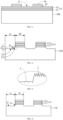
- Some embodiments of the present disclosure provide a method for preparing a solar cell, including: providing a substrate having an initial surface and a second surface opposite to the initial surface, wherein the initial surface has a metal pattern region and a non-metal pattern region; forming, on the initial surface of the substrate, an initial first passivation contact structure and a dielectric layer stacked in a direction away from the substrate; performing a patterning process on the dielectric layer to form a first opening in the dielectric layer, wherein the first opening is aligned with the non-metal pattern region; etching the initial first passivation contact structure and the non-metal pattern region of the initial surface at the first opening to form a first surface having the non-metal pattern region and the metal pattern region, wherein the non-metal pattern region includes a first region and a second region adjacent to the first region and to the metal pattern region; wherein the first region is closer to the second surface than the metal pattern region, and the second region is not closer to the second surface than the first region and is not further away from
- performing the patterning process on the dielectric layer includes: performing laser processing on a portion of the dielectric layer over the non-metal pattern region by using a laser process to remove the portion of the dielectric layer over the non-metal pattern region so as to form the first opening, wherein the first opening exposes a portion of the initial first passivation contact structure over the non-metal pattern region.
- performing the patterning process on the dielectric layer includes: forming an ink layer on a top surface of a portion of the dielectric layer over the initial metal pattern region, wherein the ink layer is aligned with the initial metal pattern region; and performing pickling processing on the dielectric layer to remove a portion of the dielectric layer over the initial non-metal pattern region so as to form the first opening, wherein the first opening exposes a portion of the initial first passivation contact structure over the initial non-metal pattern region.
- performing a doping process at the first region and the second region includes: implanting a doped element at the first region and the second region, so that the doped element is diffused into a portion of the substrate corresponding to the first region and the second region to form an initial doped layer having a preset thickness; and performing an annealing process on the initial doped layer to form the doped layer.
- a concentration of the doped element in a portion of the doped layer corresponding to the second region is gradually reduced in a direction approaching the second surface.
- the first passivation contact structure is disposed on the portion of the substrate corresponding to the metal pattern region.
- the metal pattern region is a region configured to form the metal electrode, that is, the metal electrode is in electrical contact with the first passivation contact structure, so as to reduce the contact recombination loss of the metal electrode and improve the performance of the solar cell.
- the doping layer is formed in the portion of the substrate corresponding to the non-metal electrode region, and the doping layer achieves the selective transmission of carriers or forms an internal electric field in the substrate.
- the doping layer and the substrate have the same material, which greatly reduces the parasitic absorption of incident light by the doping layer, and further improves the utilization rate of incident light.
- the first region and the second region of the non-metal pattern region and the metal pattern region are successively connected, and the substrate has a height in the second region between that in the first region and that in the metal pattern region, so that the surface of the substrate in the first region, the second region and the metal pattern region forms a step morphology.
- the top surface of the doping layer formed in the portion of the substrate corresponding to the first region and the second region also has a partial step morphology.
- the area of the doping layer is increased, which is conducive to increasing an action area of the doping layer, thus improving the photoelectric conversion performance of the solar cell.
- a surface of the substrate of the solar cell has a metal pattern region and a non-metal pattern region.
- a metal pattern region in which a metal electrode needs to be disposed, contact recombination loss of the metal electrode needs to be reduced, and for the non-metal pattern region, parasitic absorption of incident light needs to be reduced to improve absorptivity of the incident light.
- a doped layer is typically provided to form a PN junction with a substrate or to enhance transmission of carriers in the substrate in the non-metal pattern region.
- an area of the doped layer in the non-metal pattern region needs to be increased, so as to improve the carrier transmission capacity.
- film layers formed over the non-metal pattern region of the surface of the substrate may have poor flatness, which is not conducive to improving performance of the film layers. That is to say, structures of different film layers are unbale to be balanced in the conventional solar cell, so that other performance may be sacrificed while improving a certain performance of the solar cell. Therefore, overall photoelectric conversion performance of the solar cell is poor.
- Embodiments of the present disclosure provides a solar cell in which the first passivation contact structure is disposed on the portion of the substrate corresponding to the metal pattern region.
- the metal pattern region is a region configured to form the metal electrode, that is, the metal electrode is in electrical contact with the first passivation contact structure, so as to reduce the contact recombination loss of the metal electrode and improve the performance of the solar cell.
- the doping layer is formed in the portion of the substrate corresponding to the non-metal electrode region, and the doping layer achieves the selective transmission of carriers or forms an internal electric field in the substrate.
- the doping layer and the substrate have the same material, which greatly reduces the parasitic absorption of incident light by the doping layer, and further improves the utilization rate of incident light.
- the first region and the second region of the non-metal pattern region and the metal pattern region are successively connected, and the substrate has a height in the second region between that in the first region and that in the metal pattern region, so that the surface of the substrate in the first region, the second region and the metal pattern region forms a step morphology.
- the top surface of the doping layer formed in the portion of the substrate corresponding to the first region and the second region also has a partial step morphology.
- the area of the doping layer is increased, which is conducive to increasing an action area of the doping layer, thereby ensuring high utilization of the incident light by the solar cell while reducing the contact recombination loss of the metal electrode, and further increasing an active area of the doped layer and improving the overall photoelectric conversion performance of the solar cell.
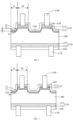
- FIG. 1 is a schematic cross-sectional structural diagram of a solar cell according to an embodiment of the present disclosure.
- the solar cell includes a substrate 100, a doped layer 120, and a first passivation contact structure.
- the substrate 100 has a first surface and a second surface opposite to the first surface, and the first surface has a metal pattern region 10 and a non-metal pattern region 11.
- the non-metal pattern region 11 includes a first region 12 and a second region 13 adjacent to the first region and to the metal pattern region 10.
- the first surface of the substrate 100 in the first region 12 is lower than the first surface of the substrate 100 in the metal pattern region 10
- the first surface of the substrate 100 in the second region 13 is not lower than the first surface of the substrate 100 in the first region 12 and is not higher than the first surface of the substrate 100 in the metal pattern region 10.
- the first region 12 of the first surface is closer to the second surface of the substrate 100 than the metal pattern region 10 of the first surface
- the second region 13 of the first surface is not closer to the second surface than the first region 12 of the first surface and is not further away from the second surface than the metal pattern region 10 of the first surface.
- the doped layer 120 is formed in a portion of the substrate 100 corresponding to the first region 12 and the second region 13, and the doped layer 120 has a top surface exposed out of the substrate 100. That is, the doped layer 120 has a top surface at the first region 12 and the second region 13.
- the first passivation contact structure 110 covers the metal pattern region 10 of the first surface, and the first passivation contact structure includes at least one first passivation contact substructure, and each of the at least one first passivation contact substructure includes a first tunneling layer and a first doped conductive layer stacked in a direction away from the substrate 100.
- the first passivation contact structure 110 is only provided over the metal pattern region 10 of the first surface, so that the metal contact recombination between the first passivation contact structure 110 and a metal electrode is able to be reduced if the metal electrode is provided in the metal pattern region 10, thereby improving the carrier collection capability of the metal electrode.
- the doped layer 120 is formed in the portion of the substrate 100 corresponding to the non-metal pattern region 11, that is, the doped layer 120 and the substrate 100 are of the same type of material, and the substrate 100 has a weak parasitic absorption capability on incident light, so that the parasitic absorption capability of the doped layer 120 on incident light is weak.
- the first passivation contact structure 110 also being provided over the non-metal pattern region 11 of the first surface of the substrate 100
- the parasitic absorption of the non-metal pattern region 11 of the first surface of the substrate 100 on incident light is able to be reduced, thereby improving the utilization rate of incident light.
- the doped layer 120 is also able to form a PN junction with the substrate 100 or achieve selective transmission of carriers.
- the first region 12 and the second region 13 of the non-metal pattern region 11, and the metal pattern region 10 are successively connected, and a portion of the substrate 100 corresponding to the second region 13 has a height between a height of a portion of the substrate 100 corresponding to the first region 12 and a height of a portion of the substrate 100 corresponding to the metal pattern region 10, such that the first region 12, the second region 13, and the metal pattern region 10 form the first surface of a step shape.
- the doped layer 120 is formed in the portion of the substrate 100 corresponding to the first region 12 and the second region 13, and the top surface of the doped layer 120 is exposed out of the substrate 100 (i.e., the doped layer 120 has a top surface at the first region 12 and the second region 13), so that the top surface of the doped layer 120 also has a partial step morphology.
- the surface of the doped layer 120 being a flat surface, a surface area of the doped layer 120 is increased, thereby increasing an action area of the doped layer 120, and further improving the performance of the doped layer 120.
- the second region 13 is actually a transition region between the first region 12 and the metal pattern region 10, and it is the presence of the second region 13 that the surface area of the doped layer 120 is increased.
- the textured structure does not need to be prepared over the first region 12 of the non-metal pattern region 11 of the first surface, so that the surface area of the doped layer 120 is increased, and the first surface in the first region 12 is relatively flat. If the first passivation layer is formed over the first region 12 of the first surface, the flatness of the formed first passivation layer is improved, thereby improving the passivation performance of the first passivation layer on the first surface of the substrate 100, and further improving the photoelectric conversion performance of the solar cell.
- the second region 13 is adjacent to the metal pattern region 10, so that an area of the doped layer 120 close to the metal pattern region 10 is relatively large. If the doped layer 120 plays a carrier transmission role, a path that carriers transmitting from the doped layer 120 to the first passivation contact structure 110 over the metal electrode portion 10 is relatively short, so that the transmission performance of carriers is enhanced.
- the first surface of the substrate 100 has a step shape, which increases the surface area of the first surface of the substrate 100 in a height direction, so that the area of the doped layer 120 is increased while a cross-sectional area of the surface of the substrate 100 is not increased, thereby keeping assembly density of a photovoltaic module large when the solar cell is assembled to form the photovoltaic module, which is beneficial to keeping higher module power.
- the height direction herein refers to a direction in which the first passivation contact structure 110 points to the substrate 100, i.e., a direction perpendicular to the second surface of the substrate 100.
- the cross-sectional area is a cross-sectional area in a direction parallel to the second surface of the substrate 100.
- the first region 12 and the second region 13 are provided in the non-metal pattern region 11, the first region 12, the second region 13 and the metal pattern region 10 form a step shape, and the doped layer 120 is formed in the portion of the substrate 100 corresponding to the first region 12 and the second region 13, so that the solar cell has a high utilization rate of incident light while the contact recombination loss of the metal electrode is reduced, the action area of the doped layer 120 is also increased, and the overall photoelectric conversion performance of the solar cell is improved.
- the structural arrangement of the doped layer 120, the surface of the substrate 100 having the step shape and the first passivation contact structure 110 advantages of the doped layer 120 and the first passivation contact structure 110 are exerted, adverse effects of the doped layer 120 and the first passivation contact structure 110 on other structures of the solar cell are reduced to a greater extent, and the overall performance of the solar cell is synergistically improved.
- the height of the first surface in the first region 12 of the non-metal pattern region 11, the height of the first surface in the second region 13, and the height of the first surface in the metal pattern region 10 are all relative to the other opposite surface of the substrate 100 (i.e., the second surface).
- a surface on which the first passivation contact structure 110 is disposed is the first surface of the substrate 100
- a surface of the substrate 100 away from the first passivation contact structure 110 is the second surface.
- the first surface and the second surface are opposite to each other.
- the height of the first surface in the first region 12 of the non-metal pattern region 11, the height of the first surface in the second region 13, and the height of the first surface in the metal pattern region 10 are all relative to the second surface.
- a thickness of a portion of the substrate 100 corresponding to the first region 12 is less than a thickness of a portion of the substrate 100 corresponding to the metal pattern region 10
- a thickness of a portion of the substrate 100 corresponding to the second region 13 is not less than the thickness of the portion of the substrate 100 corresponding to the first region 12, and is not greater than the thickness of the portion of the substrate 100 corresponding to the metal pattern region 10.
- the substrate 100 is configured to receive incident light and generate photogenerated carriers.
- a material of the substrate 100 may include at least one of monocrystalline silicon, polysilicon, amorphous silicon, or microcrystalline silicon.
- a material of the substrate 100 may also include silicon carbide, an organic material, or multicomponent compounds.
- the multicomponent compounds may include, but are not limited to, materials such as perovskite, gallium arsenide, cadmium telluride, copper indium selenium, and the like.
- the solar cell is a Tunnel Oxide Passivated Contact (TOPCON) cell
- the substrate 100 has two opposite surfaces, and the two opposite surfaces of the substrate 100 are able to be used to receive incident light or reflected light.
- the substrate 100 includes a doping element, and a type of the doping element includes N-type or P-type.
- the N-type element may be group V elements such as phosphorus (P), bismuth (Bi), antimony (Sb), arsenic (As), or the like.
- the P-type element may be group III elements such as boron (B), aluminum (Al), gallium (Ga), indium (In), or the like.
- the substrate 100 is a P-type substrate
- the type of the doping element in the substrate 100 is P-type.
- the substrate 100 is an N-type substrate
- the type of the doping element in the substrate 100 is N-type.
- the solar cell further includes a first electrode 130, and the first electrode 130 is electrically connected to a first doped conductive layer 112.
- the photogenerated carriers generated in the substrate 100 are transmitted from the substrate 100 to the first doped conductive layer 112 and then transmitted to the first electrode 130, and the first electrode 130 is configured to collect photogenerated carriers.
- the first electrode 130 is disposed in the metal pattern region 10.
- the doped element in the first doped conductive layer 112 and the doped element in the doped layer 120 are congeners (i.e., elements of the same group).
- the doped element in the first doped conductive layer 112 and the doped element in the doped layer 120 are both be a Group III element, for example, may be boron, gallium, or indium.
- the doped element in the first doped conductive layer 112 and the doped element in the doped layer 120 are both Group V elements, for example, may be phosphorus, arsenic, or antimony.
- a type of the doped element in the first doped conductive layer 112 is the same as a type of the doped element in the doped layer 120, and may be both a P-type doped element or an N-type doped element.
- the doped element in the first doped conductive layer 112 and the doped element in the doped layer 120 are provided as congeners, i.e., an outermost electron number of the doped element in the first doped conductive layer 112 is consistent with an outermost electron number of the doped element in the doped layer 120, so that chemical properties of the first doped conductive layer 112 and the doped layer 120 are similar, thereby enhancing the transmission performance of carriers from the doped layer 120 to the first doped conductive layer 112.
- a concentration of the doped element in the first doped conductive layer 112 is greater than or equal to a concentration of the doped element in the doped layer 120. In some embodiments, the concentration of the doped element in the first doped conductive layer 112 is greater than the concentration of the doped element in the doped layer 120, and is greater than a concentration of the doped element in the substrate 100.
- the first doped conductive layer 112 forms a heavily doped region relative to the substrate 100, so that carriers in the substrate 100 generate a barrier effect, the transmission capability of carriers from the substrate 100 to the first doped conductive layer 112 is enhanced while the tunneling capability of carriers in the first tunneling layer 111 is enhanced, which is conducive to increasing the carrier concentration and is conducive to collection of carriers by the first electrode 130.
- the concentration of the doped element in the doped layer 120 is small, so that the doped layer 120 has a good surface passivation effect on the substrate 100. Moreover, a doping concentration difference between the concentration of the doped element in the doped layer 120 and the concentration of the doped element in the first doped conductive layer 112 is able to enhance lateral transmission of carriers between the doped layer 120 and the first doped conductive layer 112, thereby further improving the collection capability of carriers.
- the concentration of the doped element in the first doped conductive layer 112 is in a range of 1 ⁇ 10 19 atoms/cm 3 to 9 ⁇ 10 20 atoms/cm 3
- the concentration of the doped element in the doped layer 120 is in a range of 1 ⁇ 10 16 atoms/cm 3 to 1 ⁇ 10 20 atoms/cm 3 .
- the concentration of the doped element in the first doped conductive layer 112 may be in a range of 1 ⁇ 10 19 atoms/cm 3 to 5 ⁇ 1 0 19 atoms/cm 3 , 5 ⁇ 10 19 atoms/cm 3 to 9 ⁇ 1 0 19 atoms/cm 3 , 9 ⁇ 10 19 atoms/cm 3 to 1 ⁇ 10 20 atoms/cm 3 , 1 ⁇ 10 20 atoms/cm 3 to 2 ⁇ 10 20 atoms/cm 3 , 2 ⁇ 10 20 atoms/cm 3 to 4 ⁇ 10 20 atoms/cm 3 , 4 ⁇ 10 20 atoms/cm 3 to 5 ⁇ 10 20 atoms/cm 3 , 5 ⁇ 10 20 atoms/cm 3 to 6 ⁇ 10 20 atoms/cm 3 , 6 ⁇ 10 20 atoms/cm 3 to 8 ⁇ 10 20 atoms/cm 3 , or 8 ⁇ 10 20 atoms/cm 3 to 9 ⁇ 10
- the concentration of the doped element in the doped layer 120 may be in a range of 1 ⁇ 10 16 atoms/cm 3 to 5 ⁇ 10 16 atoms/cm 3 , 5 ⁇ 10 16 atoms/cm 3 to 9 ⁇ 10 16 atoms/cm 3 , 9 ⁇ 10 16 atoms/cm 3 to 1 ⁇ 10 17 atoms/cm 3 , 1 ⁇ 10 17 atoms/cm 3 to 1 ⁇ 10 18 atoms/cm 3 , 1 ⁇ 10 18 atoms/cm 3 to 5 ⁇ 10 18 atoms/cm 3 , 5 ⁇ 10 18 atoms/cm 3 to 9 ⁇ 10 18 atoms/cm 3 , 9 ⁇ 10 18 atoms/cm 3 to 1 ⁇ 10 19 atoms/cm 3 , 1 ⁇ 10 19 atoms/cm 3 to 5 ⁇ 10 19 atoms/cm 3 , 5 ⁇ 10 19 atoms/cm 3 to 9 ⁇ 10 19 atoms/cm 3 , or 9 ⁇ 10 19
- the concentration of the doped element in the first doped conductive layer 112 is large, which is conducive to enhancing the transmission of carriers in the first doped conductive layer 112 and the tunneling of carriers in a first tunneling layer 111. Moreover, within the above ranges, the concentration of the doped element in the doped layer 120 is small, so that the doped layer 120 has a good surface passivation effect on the first surface of the substrate 100 in the non-metal pattern region 11, and the carrier recombination on the first surface of the substrate 100 in the non-metal pattern region 11 is reduced.
- the concentration of the doped element in the first doped conductive layer 112 is greater than the concentration of the doped element in the doped layer 120, so that the first doped conductive layer 112 is also able to form a heavily doped region relative to the doped layer 120, thereby enabling carriers in the doped layer 120 to generate a barrier effect, and enhancing the transmission capability of carriers from the doped layer 120 to the first doped conductive layer 112, which is conducive to enhancing the collection capability of carriers.
- the concentration of the doped element in the doped layer 120 is equal to the concentration of the doped element in the first doped conductive layer 112.
- the type of the doped element in the doped layer 120 is different from the type of the doped element in the substrate 100. That is, the doped layer 120 serves as an emitter and forms a PN junction with the substrate 100. The PN junction is used to receive incident light and generate photogenerated carriers, the generated photogenerated carriers are transmitted from the substrate 100 to the first doped conductive layer 112 and then transmitted to the first electrode 130, and the first electrode 130 is configured to collect the photogenerated carriers. The photogenerated carriers may also be transmitted in the doped layer 120, i.e., transmitted from the doped layer 120 to the first doped conductive layer 112, and then collected by the first electrode 130.
- the type of the doped element in the first doped conductive layer 112 is the same as the type of the doped element in the doped layer 120, that is, the type of the doped element in the first doped conductive layer 112 is also different from the type of the doped element in the substrate 100, so that the first doped conductive layer 112 is also able to form a PN junction with the substrate 100, thereby increasing the number of generated photogenerated carriers, and improving concentration of the carriers, the filling factor, and a short-circuit current and an open-circuit voltage.
- the arrangement of the first doped conductive layer 112 being only disposed over the metal pattern region 10 of the first surface to form a PN junction with the substrate 100 and the first electrode 130 being electrically connected to the first doped conductive layer 112 reduces the metal contact recombination of the first electrode 130, and improve the carrier collection capability of the first electrode 130.
- the arrangement of the doped layer 120 being provided in the portion of the substrate 100 corresponding to the non-metal pattern region 11, the doped layer 120 and the substrate 100 forming a PN junction, and the material of the doped layer 120 being the same as that of the substrate 100 greatly reduces the parasitic absorption of the portion of the substrate 100 corresponding to the non-metal pattern region 11 on incident light, thereby improving the utilization rate of incident light.
- both the type of the doped element in the doped layer 120 and the type of the doped element in the first doped conductive layer 112 are P-type, for example, may be phosphorus, bismuth, antimony, or arsenic, and the type of the doped element in the substrate 100 is N-type, for example, may be boron, gallium, or gallium.
- the concentration of the doped element in the doped layer 120 is greater than the concentration of the doped element in the substrate 100. In other words, the concentration of the doped element in the doped layer 120 is greater than the concentration of the doped element in a portion of the substrate 100 other than the doped layer 120. In this way, the doped layer 120 is heavily doped than the portion of the substrate 100 other than the doped layer 120, so that a concentration gradient of the same type of doped element is established between the doped layer 120 and the portion of the substrate 100 other than the doped layer 120, so as to form a rear electric field, and the presence of the rear electric field allows effective collection of photogenerated carriers.
- the doped layer 120 is disposed in a portion of the substrate 100 corresponding to the first region 12 and the second region 13, a top surface of the doped layer 120 has a partial step morphology, thereby increasing the surface area of the doped layer 120. And if the doped layer 120 serves as the emitter of the solar cell, the area of the formed PN junction is accordingly increased, so that the number of photogenerated carriers generated by the PN junction is increased, the carrier concentration is further improved, and the open-circuit voltage and the short-circuit current are improved.
- the doped layer 120 if the doped layer 120 serves as the PN junction, the doped layer 120 needs to be in contact with the incident light as much as possible, so that more incident light irradiates the top surface of the doped layer 120.
- the first surface of the substrate 100 in the second region 13 is inclined relative to the first surface of the substrate 100 in the first region 12, and an included angle formed between the first surface of the substrate 100 in the second region 13 and the first surface of the substrate 100 in the first region 12 is an obtuse angle, so that the first surface of the substrate 100 in the second region 13 is exposed to the outside as much as possible, thereby reducing the shielding of the first surface of the substrate 100 in the second region 13, and further improving the utilization rate of the incident light by the substrate 100.
- the arrangement of the first surface of the substrate 100 in the second region 13 being inclined relative to the first surface of the substrate 100 in the first region 12 a surface area of the first surface of the substrate 100 in the second region 13 is increased when the height difference between the first surface of the substrate 100 in the first region 12 and the first surface of the substrate 100 in the metal pattern region 10 is certain, thereby further increasing the surface area of the doped layer 120.
- a first included angle ⁇ is formed between the first region 12 and the second region 13 of the first surface of the substrate 100, and the first included angle ⁇ is in a range of 90° to 160°, for example, 90° to 95°, 95° to 100°, 100° to 105°, 105° to 110°, 110° to 115°, 115° to 120°, 120° to 125°, 125° to 130°, 130° to 135°, 135° to 140°, 140° to 145°, 145° to 150°, 150° to 155° or 155° to 160°.
- the first surface of the substrate 100 in the second region 13 is inclined relative to the first surface of the substrate 100 in the first region 12, so that the first surface of the substrate 100 in the second region 13 has a large surface area, thereby further increasing the surface area of the doped layer 120.
- the doped layer 120 serves as the emitter of the solar cell, the area of the formed PN junction is increased, thereby generating more photogenerated carriers and improving the photoelectric performance of the solar cell.
- the first surface of the substrate 100 in the first region 12 is perpendicular to the first surface of the substrate 100 in the second region 13.
- a height difference 'd' between the metal pattern region 10 and the first region 12 of the first surface of the substrate 100 is in a range of 0.1 ⁇ m to 10 ⁇ m, for example, 01 ⁇ m to 0.2 ⁇ m, 0.2 ⁇ m to 0.5 ⁇ m, 0.5 ⁇ m ⁇ 1 ⁇ m, 1 ⁇ m to 1.5 ⁇ m, 1.5 ⁇ m to 2 ⁇ m, 2 ⁇ m to 2.5 ⁇ m, 2.5 ⁇ m to 3 ⁇ m, 3 ⁇ m to 3.1 ⁇ m, 3.1 ⁇ m to 3.2 ⁇ m, 3.2 ⁇ m to 3.5 ⁇ m, 3.5 ⁇ m to 3.8 ⁇ m, 3.8 ⁇ m to 3.9 ⁇ m, 3.9 ⁇ m to 4 ⁇ m, 4 ⁇ m to 4.5 ⁇ m, 4.5 ⁇ m to 5 ⁇ m, 5 ⁇ m to 5.5 ⁇ m, 5.5 ⁇ m to 6 ⁇ m, 6 ⁇ m to 6.5 ⁇ m, 6.5 ⁇ m to 7 ⁇ m, 7 ⁇ m to 7.5 ⁇ m, 7.5 ⁇ m to 8 ⁇ m, 8 ⁇ m
- the height difference 'd' between the first region 12 and the metal pattern region 10 of the first surface of the substrate 100 is large, so that the first surface of substrate 100 in the second region 13 has a large surface area, thus making the surface area of the doping layer 120 larger and improving the capability of the doped layer 120 to generate photogenerated carriers when serving as the emitter.
- the height difference 'd' between the first region 12 and the metal pattern region 10 of the first surface of the substrate 100 is not excessively large, so that the problem of too much defect state density on the first surface of the substrate 100 due to excessive etching of the substrate 100 in the process of actually forming the first region 12, the second region 13 and the metal pattern region 10 of the first surface of the substrate 100 is avoided, thus the carrier recombination on the first surface of the substrate 100 is less, which is conducive to improving the filling factor of the solar cell.
- a concentration of the doped element in a portion of the doped layer 120 corresponding to the second region 13 is not less than a concentration of the doped element in a portion of the doped layer 120 corresponding to the first region 12, and is not greater than a concentration of the doped element in the first doped conductive layer 112.
- the concentration of the doped element in the portion of the doped layer 120 corresponding to the second region 13 is greater than the concentration of the doped element in the portion of the doped layer 120 corresponding to the first region 12, and the concentration of the doped element in the portion of the doped layer 120 corresponding to the second region 13 is less than the concentration of the doped element in the first doped conductive layer 112.
- the concentration of the doped element in the portion of the doped layer 120 corresponding to the second region 13 is between the concentration of the doped element in the portion of the doped layer 120 corresponding to the first region 12 and the concentration of the doped element in the first doped conductive layer 112.
- the presence of the portion of the doping layer 120 corresponding to the second region 13 avoids low efficiency of carrier lateral transmission caused by excessively large potential energy difference between the portion of the doping layer 120 corresponding to the first region 12 and the first doping conductive layer 112 over the metal pattern region 10 due to the carrier transmission in the first doped conductive layer 112 and the doping layer 120 which have a large difference in the concentration of the doped element.
- the portion of the doped layer 120 corresponding to the second region 13 plays a transition role, which reduces the potential energy difference of the carriers transmitted between the portion of the doped layer 120 corresponding to the first region 12 and the first doped conductive layer 112, thereby ensuring the validity of the carrier lateral transmission and improving the filling factor of the solar cell.
- a concentration of the doped element in the portion of the doped layer 120 corresponding to the second region 13 gradually decreases in a direction from a side of the portion of the doped layer 120 corresponding to the first region 12 facing the first doped conductive layer 112 toward a side of the portion of the doped layer 120 corresponding to the first region 12 away from the first doped conductive layer 112, i.e., in a direction approaching the second surface.
- the concentration of the doped element in the portion of the doped layer 120 corresponding to the second region 13 is gradually changed, so that the potential energy difference of the carriers transmitted between the portion of the doped layer 120 corresponding to the first region 12 and the first doped conductive layer 112 is further reduced, thereby improving the lateral transmission capability of carriers.
- the height of the first surface of the substrate 100 in the second region 13 is not lower than the height of the first surface of the substrate 100 in the first region 12, such that the first surface of the substrate 100 in the second region 13 and the first surface of the substrate 100 in the first region 12 form a partial step morphology.
- the first surface of the substrate 100 in the second region 13 is perpendicular or inclined relative to the first surface of the substrate 100 in the first region 12, that is, the first surface of the substrate 100 in the second region 13 has a height difference in a direction perpendicular to the first surface of the substrate 100 in the first region 12.
- a doped rate of the doped element in the portion of the substrate 100 corresponding to the second region 13 is inconsistent in the direction perpendicular to the first surface of the substrate 100 in the first region 12, thereby facilitating the formation of the portion of the doped layer 120 corresponding to the second region 13, in which the doped element is gradually changed, for example, facilitating the formation of the portion of the doped layer 120 corresponding to the second region 13, in which the doped element gradually decreases in the direction of the portion of the doped layer 120 corresponding to towards the first doped conductive layer 112, i.e., in the direction approaching the second surface.
- a concentration of the doped element at a side of the portion of the doped layer 120 corresponding to the second region 13 facing the first doped conductive layer 112 is different from a concentration of the doped element at a side of the portion of the doped layer 120 corresponding to the second region 13 away from the first doped conductive layer 112 by 1 ⁇ 10 19 atoms/cm 3 to 8 ⁇ 10 20 atoms/cm 3 , i.e., a concentration of the doped element at a side of the portion of the doped layer 120 corresponding to the second region 13 away from the second surface is different from a concentration of the doped element at a side of the portion of the doped layer 120 corresponding to the second region 13 closer to the second surface by 1 ⁇ 10 19 atoms/cm 3 to 8 ⁇ 10 20 atoms/cm 3 , for example, may be 1 ⁇ 10 19 atoms/cm 3 to 3 ⁇ 10 19 atoms/cm 3 , 3 ⁇ 10 19 atoms/cm
- the concentration of the doped element at the side of the portion of the doped layer 120 corresponding to the second region 13 facing the first doped conductive layer 112, i.e., the concentration of the doped element at the side of the portion of the doped layer 120 corresponding to the second region 13 away from the second surface is equal to the concentration of the doped element in the first doped conductive layer 112 and the concentration of the doped element at the side of the portion of the doped layer 120 corresponding to the second region 13 away from the first doped conductive layer 112, i.e., the concentration of the doped element at the side of the portion of the doped layer 120 corresponding to the second region 13 closer to the second surface, is equal to the concentration of the doped element in the portion of the doped layer 120 corresponding to the first region 12.
- the potential energy difference of the carriers at a contact interface between the portion of the doped layer 120 corresponding to the second region 13 and the first doped conductive layer 112 is reduced, and the potential energy difference of the carriers at a contact interface of the portion of the doped layer 120 corresponding to the second region 13 and the portion of the doped layer 120 corresponding to the first region 12 is reduced, which are conducive to further improving the lateral transmission capability of carriers.
- the concentration of the doped element in the portion of the doped layer 120 corresponding to the second region 13 is equal to the concentration of the doped element in the portion of the doped layer 120 corresponding to the first region 12 and the concentration of the doped element in the first doped conductive layer 112.
- a square resistance of the doped layer 120 is able to be adjusted. For example, when the concentration of the doped element in the overall doped layer 120 is low, the square resistance of the doped layer 120 is able to be adjusted to be large, so that carrier recombination centers on the surface of the doped layer 120 are less, the recombination of carriers on the surface of the doped layer 120 is reduced, and the carrier concentration is increased, thereby increasing the open-circuit voltage and the filling factor of the solar cell, and improving the conversion efficiency of the solar cell.
- the square resistance of the doped layer 120 is in a range of 80ohm/sq to 1000ohm/sq, for example, 80ohm/sq to 100ohm/sq, 100ohm/sq to 130ohm/sq, 130ohm/sq to 150ohm/sq, 150ohm/sq to 280ohm/sq, 280ohm/sq to 450ohm/sq, 450ohm/sq to 600ohm/sq, 600ohm/sq to 720ohm/sq, 720ohm/sq to 850ohm/sq, 850ohm/sq to 900ohm/sq, 900ohm/sq to 950ohm/sq, or 950ohm/sq to 1000ohm/sq.
- carrier recombination centers generated on the surface of the doped layer 120 are less, so that the carrier concentration is increased, and the transmission capability of the carriers is improved, thereby increasing the open-circuit voltage and the filling factor of the solar cell, and improving the conversion efficiency of the solar cell.
- the first surface of the substrate 100 is provided with a first texture structure in the metal pattern region 10 and a second texture structure in the non-metal pattern region 11, and a roughness of the first texture structure is greater than a roughness of the second texture structure.
- the roughness of the first texture structure is large, so that a surface area of the first surface of the substrate 100 in the metal pattern region 10 is large, and the first passivation contact structure 110 formed over the metal pattern region 10 of the first surface of the substrate 100 is able to maintain the morphology of the first surface of the substrate 100 in the metal pattern region 10.
- a top surface of the first passivation contact structure 110 also has a large roughness, and the surface area of the first passivation contact structure 110 is increased, so that a contact area of the first electrode 130 formed in the first passivation contact structure 110 and the first passivation contact structure 110 is large, a contact resistance of the first electrode 130 is reduced, thereby improving the carrier transmission performance.
- the surface area of the first surface of the substrate 100 is increased in the height direction, and therefore, the roughness of the second texture structure is set to be small, so that the first surface of the substrate 100 in the non-metal pattern region 11 is relatively flat.
- the first passivation layer is able to uniformly cover the surface of the doped layer 120 in the process of forming the first passivation layer, so that the morphology of the first passivation layer is relatively flat, a morphology of an interface between the first passivation layer and the surface of the doped layer 120 is improved, and the interface state density is reduced.
- This not only helps to reduce the recombination of carriers on the surface of the doped layer 120 corresponding to the non-metal pattern region 11, but also enhances the tunneling capability of carriers, thereby increasing the number of carriers and improving the photoelectric conversion performance of the solar cell.
- the first texture structure includes a pyramid structure
- the second texture structure includes a platform protrusion structure.
- the pyramid structure includes a tetrahedron, an approximate tetrahedron, a pentahedron, an approximate pentahedron, or the like.
- the platform protrusion structure includes a base portion of the pyramid structure, i.e., a remaining bottom portion of the pyramid structure after removing a tip portion.
- the second texture structure includes a platform protrusion-like structure
- a top surface of the platform protrusion-like structure may be a flat plane or an inclined plane
- a bottom surface of the platform protrusion structure may be a polygonal plane, for example, may be a quadrilateral plane or a pentagonal plane.
- the first passivation contact structure 110 includes a plurality of first passivation contact substructures 113 stacked in a direction away from the substrate 100, and each of the first passivation contact substructures 113 includes a first tunneling layer 111 and a first doped conductive layer 112 stacked in a direction away from the substrate 100. That is to say, each first tunneling layer 111 in the plurality of first tunneling layers 111 in the first passivation contact structure 110 is alternately stacked with each first doped conductive layer 112 in the plurality of first doped conductive layers 112 in the first passivation contact structure 110.
- the first passivation contact structure 110 include only one first tunneling layer 111 and one first doped conductive layer 112, and the first tunneling layer 111 is formed on the first surface of the substrate 100.
- the first tunneling layer 111 provides a tunneling channel for carriers and enhances the selective transmission capability of carriers.
- a material of the first doped conductive layer 112 includes at least one of amorphous silicon, polycrystalline silicon, and silicon carbide.
- a material of the first tunneling layer 111 includes at least one of silicon oxide, aluminum oxide, silicon nitride, silicon oxynitride, amorphous silicon, or polycrystalline silicon.
- the solar cell further includes a second passivation contact structure 150, the second passivation contact structure 150 is formed on a surface of the substrate 100 away from the first passivation contact structure 110, i.e., the second surface, and the second passivation contact structure 150 includes at least one second tunneling layer 151 and at least one second doped conductive layer 152 stacked in a direction away from the substrate 100.
- a second doped conductive layer 152 has a field passivation effect, so that minority carriers escape from the interface, thereby reducing a concentration of minority carriers, and enabling a recombination rate of carriers at the interface of the substrate 100 to be relatively low, so that the open-circuit voltage, the short-circuit current and the filling factor of the solar cell are large, and the photoelectric conversion performance of the solar cell is improved.
- a type of the doped element in the first doped conductive layer 112 is different from a type of the doped element in the substrate 100, and a type of the doped element in the second doped conductive layer 152 is the same as the type of the doped element in the substrate 100.
- a concentration of the doped element in the second doped conductive layer 152 is greater than the concentration of the doped element in the substrate 100, and the second doped conductive layer 152 forms a high-low junction with the substrate 100, which is beneficial to forming the barrier effect of carriers, thereby enhancing the transmission of carriers.
- the second tunneling layer 151 is configured to realize the interface passivation of the second surface of the substrate 100, which achieves a chemical passivation effect. Specifically, the interface defect state density of the second surface of the substrate 100 is reduced by saturating suspension keys on the second surface of the substrate 100, thereby reducing recombination centers on the second surface of the substrate 100.
- the second passivation contact structure 150 includes only one second tunneling layer 151 and one second doped conductive layer 152 stacked in a direction away from the substrate 100.
- the second passivation contact structure 150 includes a plurality of second passivation contact substructures stacked in a direction away from the substrate 100, and each of the plurality of second passivation contact substructures includes a second tunneling layer 151 and a second doped conductive layer 152 stacked in a direction away from the substrate 100. That is, each second tunneling layer 151 in the plurality of second tunneling layers 151 in the second passivation contact structure 150 is alternately stacked with each second doped conductive layer 152 in the plurality of second doped conductive layers 152 in the second passivation contact structure 150.
- the solar cell further includes a first passivation layer 140, and the first passivation layer 140 is disposed on a top surface of the doped layer 120 and a top surface and side surfaces of the first passivation contact structure 110.
- the first passivation layer 140 is disposed on the top surface of the doped layer 120 corresponding to the first region 12 and the second region 13, so that a good passivation effect is achieved on the first surface of the substrate 100 in the non-metal pattern region 11. Better chemical passivation is performed on the suspension keys on the first surface of the substrate 100 in the non-metal pattern region 11, so that the defect state density of the first surface of the substrate 100 in the non-metal pattern region 11 is reduced, carrier recombination on the first surface of the substrate 100 in the non-metal pattern region 11 is inhibited, and the carrier concentration is improved.
- the first passivation layer 140 is disposed on the top surface and the side surfaces of the first passivation contact structure 110, i.e., the first passivation layer 140 covers the top surface and the side surfaces of the first passivation contact structure 110, which has a better passivation effect on the first surface of the substrate 100 in the metal pattern region 10, the top surface and side surfaces of the first doped conductive layer 112 and side surfaces of the first tunneling layer 111, and inhibits the carrier recombination on the first surface of the substrate 100 in the metal pattern region 10, the carrier recombination on the surface of the first doped conductive layer 112 and the carrier recombination on the side surfaces of the first tunneling layer 111, improves the concentration of carriers in the first surface of the substrate 100 in the metal pattern region 10, the first doped conductive layer 112 and the first tunneling layer 111, and enhances the carrier collection capability of the first electrode 130.
- a height of a portion of the first passivation layer 140 on the top surface of the portion of the doped layer 120 corresponding to the first region 12 is lower than a height of the first passivation layer 140 over the metal pattern region 10, and a height of a portion of the first passivation layer 140 on the top surface of the portion of the doped layer 120 corresponding to the second region 13 is between the height of the portion of the first passivation layer 140 on the top surface of the portion of the doped layer 120 corresponding to the first region 12 and the height of the first passivation layer 140 over the metal pattern region 10, i.e., the top surface of the first passivation layer 140 also has a step morphology.
- the height of the portion of the first passivation layer 140 on the top surface of the portion of the doped layer 120 corresponding to the first region 12 herein, the height of a portion of the first passivation layer 140 on the top surface of the portion of the doped layer 120 corresponding to the second region 13, and the height of the first passivation layer 140 over the metal pattern region 10 described here are all relative to the surface of the substrate 100 away from the first passivation layer 140, i.e., the second surface.
- the solar cell further includes a first electrode 130, and the first electrode 130 penetrates through the first passivation layer 140 to be electrically connected to the first doped conductive layer 112.
- the first electrode 130 penetrates through the first passivation layer 140 and the first doped conductive layer 112 to be electrically connected to the first tunneling layer 111.
- the solar cell further includes a second passivation layer 160, and the second passivation layer 160 is formed on a surface of the second passivation contact structure 150 away from the substrate 100.
- the second passivation layer 160 is configured to achieve a good passivation effect on the second surface of the substrate 100, reduce the defect state density of the second surface, and inhibit carrier recombination on the second surface of the substrate 100.
- the second passivation layer 160 also achieves a good anti-reflection effect, which is conducive to reducing the reflection of incident light and improving the utilization rate of incident light.
- the second passivation layer 160 includes a single-layer structure. In some embodiments, the second passivation layer 160 includes a multi-layer structure. In some embodiments, a material of the second passivation layer 160 includes at least one of silicon oxide, aluminum oxide, silicon nitride, or silicon oxynitride.
- the solar cell further includes a second electrode 170, and the second electrode 170 is disposed over the second surface of the substrate 100, and the second electrode 170 penetrates through the second passivation layer 160 to be electrically connected to the second doped conductive layer 152.
- the doped layer 120 is provided in the substrate 100, and the doped layer 120 has the same material as the substrate 100, so that the parasitic absorption of incident light by the doped layer 120 is greatly reduced.
- the passivation contact structure is formed on a portion of the substrate 100 corresponding to the metal pattern region 10, and the passivation contact structure is able to reduce the contact recombination loss of the metal electrode.
- the first region 12 and the second region 13 of the non-metal pattern region 11, and the metal pattern region 10 are sequentially connected to form the surface of the substrate 100 having a step morphology.
- the top surface of the doped layer 120 formed at the top of the substrate 100 also has a partial step morphology, which increases the area of the formed doped layer 120 and the action area of the doped layer 120, thereby ensuring the high utilization rate of the solar cell on incident light while reducing the contact recombination loss of the metal electrode, increasing the action area of the doped layer 120, and improving the overall photoelectric conversion performance of the solar cell.
- the comparation example provides a solar cell, and the difference between a structure of the solar cell provided in the comparation example and a structure of the solar cell provided in the embodiments of the present disclosure is as follows.
- the non-metal pattern region 11 of the first surface of the substrate 100 has the first region 12 and the second region 13, the first region 12 of the first surface is lower than the metal pattern region 10 of the first surface relative to the second surface, and the height of the first surface of the substrate 100 in the second region 13 is not less than the height of the first surface of the substrate 100 in the first region 12 and is not greater than the height of the first surface of the substrate 100 in the metal pattern region 10, relative to the second surface.
- the doped layer 120 is formed in the portion of the substrate 100 corresponding to the first region 12 and the second region 13, the top surface of the doped layer 120 is exposed out of the substrate 100, and the first passivation contact structure 110 is provided on the first surface of the substrate 100 in the metal pattern region 10.
- the surface of the substrate is a flat surface
- the doped layer is formed in a portion of the substrate corresponding to the metal pattern region and in a portion of the substrate corresponding to the non-metal pattern region, and the top surface of the doped layer is exposed out of the substrate.
- Table 1 Open-circuit voltage /mV Short-circuit current density /cm 2 Filling factor/% Conversion efficiency/% Embodiments of the present disclosure 722 41.51 83.34 24.98 Comparation example 709 41.66 83.11 24.54
- the open-circuit voltage, the filling factor and the conversion efficiency of the solar cell in the embodiments of the present disclosure are higher. This is because, in the embodiments of the present disclosure, only the first doped conductive layer 112 is provided on the first surface of the substrate 100 in the metal pattern region 10, and the first electrode 130 is electrically connected to the first doped conductive layer 112, so that the metal contact recombination of the first electrode 130 is reduced, and the carrier collection capability of the first electrode 130 is improved.
- the arrangement of the doped layer 120 being provided in the portion of the substrate 100 corresponding to the non-metal pattern region 11, and the material of the doped layer 120 being the same as that of the substrate 100 greatly reduces the parasitic absorption of the portion of the substrate 100 corresponding to the non-metal pattern region 11 on incident light, thereby improving the utilization rate of incident light.
- the first region 12, the second region 13, and the metal pattern region 10 of the first surface of the substrate 100 form a step morphology, which increases the area of the first surface of the substrate 100 in the non-metal pattern region 11 compared with the surface of the substrate 100 in the non-metal pattern region 11 in the comparation example, thereby increasing the portion of the doped layer 120 corresponding to the non-metal pattern region 11, ensuring that the doped layer 120 has a large action area while reducing the metal contact recombination of the metal pattern region 10, and further improving the photoelectric conversion performance of the solar cell.
- the photovoltaic module includes at least one cell string, at least one encapsulation layer 102, and at least one cover plate 103.
- Each of the at least one string is formed by connecting a plurality of solar cells 101 each provided in the above embodiments.
- Each of the at least one encapsulation layer 102 configured to cover a surface of a respective cell string.
- Each of the at least one cover plate 103 configured to cover a surface of a respective encapsulation layer 102 facing away from the respective cell string.
- the solar cells 101 are electrically connected in whole or in pieces to form a plurality of cell strings electrically connected in series and/or in parallel.
- the plurality of cell strings may be electrically connected to each other by conductive tapes 104.
- the encapsulation layers 102 covers the front surface and the rear surface (i.e., the first surface and the second surface) of the solar cell 100, respectively.
- the encapsulation layer 102 may be an organic encapsulation adhesive film such as an ethylene-vinyl acetate copolymer (EVA) adhesive film, a polyethylene octene co-elastomer (POE) adhesive film, a polyethylene terephthalate (PET) adhesive film, or the like.
- EVA ethylene-vinyl acetate copolymer
- POE polyethylene octene co-elastomer
- PET polyethylene terephthalate
- the cover plate 103 may be a glass cover plate, a plastic cover plate, or the like having a light transmitting function.
- the surface of the cover plate 103 facing towards the encapsulation layer 102 may be a concavo-convex
- a method for preparing a solar cell is further provided in the embodiments of the present disclosure.
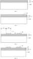
- a substrate 100 is provided, and substrate 100 has an initial surface 40 and a second surface opposite to the initial surface.
- the initial surface 40 has a metal pattern region and a non-metal pattern region.
- the metal pattern region is defined as an electrode region, and the non-metal pattern region is a region other than the metal pattern region of the surface of the substrate 100.
- the substrate 100 is configured to receive incident light and generate photogenerated carriers, and both the front surface and the rear surface of the substrate 100 may be configured to receive incident light or reflected light.
- the substrate 100 is a silicon substrate, and the material of the substrate 100 includes at least one of monocrystalline silicon, polycrystalline silicon, amorphous silicon, or microcrystalline silicon.
- the substrate 100 is an N-type semiconductor substrate, and the doped element in the substrate 100 includes any one of phosphorus, arsenic, or antimony.
- the substrate 100 is a P-type semiconductor substrate, and the doped element in the substrate 100 includes any one of boron, gallium, or indium.
- the solar cell is a TOPCON cell.
- an initial first passivation contact structure 14 and a dielectric layer 20 are stacked in a direction away from the substrate 100 on the initial surface 40 (see FIG. 5 ) of the substrate 100.
- the initial first passivation contact structure 14 is used as a basis for subsequently forming a first passivation contact structure
- the dielectric layer 20 is used as a mask for initial first passivation contact patterning for subsequently forming the first passivation contact structure.
- the method for forming the initial first passivation contact structure 14 includes forming at least one initial first tunneling layer 15 and at least one initial first doped conductive layer 16 stacked in the direction away from the substrate 100 on the initial surface 40 of the substrate 100.
- the initial first passivation contact structure 14 includes only one initial first doped conductive layer 16 and one initial first tunneling layer 15, and the formed first passivation contact structure includes only one first doped conductive layer and one first tunneling layer.
- the initial first passivation contact structure 14 includes a plurality of initial first doped conductive layers 16 and a plurality of initial first tunneling layers 15, and the initial first doped conductive layers 16 and the initial first tunneling layers 15 are alternately stacked in a direction away from the substrate 100.
- the formed first passivation contact structure includes a plurality of first doped conductive layers and a plurality of first tunneling layers, and the first doped conductive layers and the first tunneling layer are alternately stacked in a direction away from the substrate 100.
- an initial first tunneling layer 15 is formed on the initial surface of the substrate 100 by a deposition process.
- the deposition process includes any of atomic layer deposition or chemical vapor deposition.
- the material of the initial first tunneling layer 15 includes at least one of silicon oxide, aluminum oxide, silicon nitride, silicon oxynitride, amorphous silicon, or polycrystalline silicon.
- the method of forming the initial first doped conductive layer 16 includes forming a first doped layer on a surface of the initial first tunneling layer 15 by a deposition process, and implanting a doped element into the first doped layer by an in-situ deposition process during the deposition process to form an original first doped conductive layer.
- the deposition process and the process of implanting the doped element are performed at the same time, so that the process time is saved, and the process efficiency is improved.
- the original first doped conductive layer is annealed to form the initial first doped conductive layer 16.
- the doped element in the original first doped conductive layer is able to be activated to form an activated doped element.
- a type of the doped element implanted in the first doped layer is different from the type of the doped element in the substrate 100, so that the formed first doped conductive layer forms a PN junction with the substrate 100.
- the type of the doped element in the substrate 100 may be N-type, for example, may be boron, gallium, or gallium.
- the type of the doped element implanted in the first doped layer may be P-type, for example, may be phosphorus, bismuth, antimony, or arsenic.
- a material of the first doped layer includes any one of amorphous silicon, polysilicon, microcrystalline silicon, or silicon carbide.
- the method for forming the dielectric layer 20 includes forming a dielectric layer 20 on the top surface of the initial first doped conductive layer 16 by a deposition process, and the material of the dielectric layer 20 includes any one of silicon oxide, silicon nitride, aluminum oxide, or silicon oxynitride.
- the deposition process includes one of an atomic layer deposition process or a vapor deposition process.
- the initial first doped conductive layer 16 and the dielectric layer 20 are formed in the same process.
- the method for forming the initial first doped conductive layer 16 and the dielectric layer 20 includes forming the first doped layer by a deposition process, depositing a doping source on the top surface of the first doped layer, the doping source including a first doped element, and introducing oxygen while depositing the doping source. Oxygen reacts with the first doped layer to form the dielectric layer 20, and the dielectric layer 20 has the first doped element.
- the material of the first doped layer includes polysilicon, and oxygen reacts with polysilicon to generate silicon oxide. Oxygen further reacts with the first doped element.
- the first doped element is boron
- oxygen reacts with boron to generate boron oxide
- silicon oxide reacts with boron oxide to form borosilicate glass
- the borosilicate glass forms the dielectric layer 20.
- the first doped element is phosphorus
- a phosphorus-silicon glass layer is formed, and the phosphorus-silicon glass layer serves as the dielectric layer 20.
- the dielectric layer 20 is patterned to form a first opening 21 in the dielectric layer 20, and the first opening 21 is aligned with the non-metal pattern region 11.
- the patterning process of the dielectric layer 20 includes performing laser processing on a portion of the dielectric layer 20 over the non-metal pattern region 11 by using a laser process to remove the portion of the dielectric layer 20 over the non-metal pattern region 11 to form a first opening 21, and the first opening 21 exposes the initial first passivation contact structure 14 over the non-metal pattern region 11.
- the portion of the dielectric layer 20 over the non-metal pattern region 11 is removed by laser processing, thereby greatly simplifying the process and improving the process efficiency.
- a laser wavelength of the laser process is in a range of 248nm to 532nm, for example, 248nm to 255nm, 255nm to 275nm, 275nm to 290nm, 290nm to 315nm, 315nm to 340nm, 340nm to 355nm, 355nm to 370nm, 370nm to 405nm, 405nm to 445nm, 445nm to 480nm, 480nm to 495nm, 495nm to 505nm, 505nm to 520nm, or 520nm to 532nm.
- the laser energy used by the first laser process is sufficient to remove the portion of the dielectric layer 20 over the non-metal pattern region 11.
- the laser energy used by the first laser process is not too large, thereby preventing the problem of over-etching of the initial first passivation contact structure 14 covered by the dielectric layer 20 due to excessive laser energy, and ensuring that the initial first passivation contact structure 14 has a relatively flat surface.
- the patterning process of the dielectric layer 20 includes forming an ink layer 30 on the top surface of the portion of the dielectric layer 20 over the metal pattern region 10, the ink layer 30 being aligned with the metal pattern region 10 (see FIG. 9 ), and performing acid pickling treatment on the dielectric layer 20 to remove the portion of the dielectric layer 20 over the non-metal pattern region 11 to form a first opening 21, the first opening 21 exposing the portion of the initial first passivation contact structure 14 over the non-metal pattern region 11.
- the ink layer 30 is formed on a surface of a portion of the dielectric layer 20 that does not need to be removed. Since the ink layer 30 is able to be formed by processes such as coating, the pattern of the ink layer 30 is accurately controlled, thereby accurately controlling a size of the dielectric layer 20. Using the property that the ink layer 30 is insoluble in the acid, the portion of the dielectric layer 20 not covered by the ink layer 30 is removed by pickling treatment, so that a surface of the portion of the initial first passivation contact structure 14 over the non-metal pattern region 11 is exposed. The patterning process of the initial first passivation contact structure 14 is simplified through the above steps.
- the ink layer 30 is able to be formed on the surface of the portion of the dielectric layer 20 over the metal pattern region 10 by using any one of a screen-printing process, a spraying process or a 3D printing process.
- the formation of the ink layer 30 is relatively simple, and the pattern of the ink layer 30 is easy to control, which not only simplifies the process of patterning the dielectric layer 20, but also accurately controls the precision of the pattern of the formed ink layer 30, so that the morphology of each film layer in the finally formed solar cell meets the expectation, and further the photoelectric conversion performance of the solar cell meets the expectation.
- the method for pickling the dielectric layer 20 includes cleaning the surface of the dielectric layer 20 using any one of an HF solution or an HCl solution.
- the HF solution and the HCl solution have strong corrosivity, the dielectric layer 20 is able to be efficiently removed.
- a concentration of the HF solution or the HCl solution needs to be controlled to be large due to the fact that the property of the glass is relatively stable, for example, the portion of the dielectric layer 20 not covered by the ink layer 30 is able to be removed using the HF solution with a mass concentration of 50% to 70%.
- the HF solution or HCl solution is sprayed onto the surface of the dielectric layer 20 to remove the dielectric layer 20.
- the initial first passivation contact structure 14 and the non-metal pattern region 11 of the initial surface 40 of the substrate 100 are etched at the first opening 21 to form a first surface of the substrate 100 having the non-metal pattern region 11 and the metal pattern region 10, and the non-metal pattern region 11 includes a first region 12 and a second region 13 adjacent to the first region and to the metal pattern region 10.
- the first region 12 of the first surface is lower than the metal pattern region 10 of the first surface
- the second region 13 of the first surface is not lower than the first region 12 of the first surface and is not higher than the metal pattern region 10 of the first surface.
- Remaining initial first passivation contact structure 14 forms a first passivation contact structure 110.
- the initial surface 40 of the substrate refers to a surface of the substrate 100 before etching the non-metal pattern region 1 1of the surface of the substrate 100
- the formed first surface of the substrate 100 having the non-metal pattern region 11 and the metal pattern region 10 refers to a surface of the substrate 100 formed after a portion of the substrate 100 corresponding to the non-metal pattern region 11 is etched.
- the first region 12 and the second region 13 of the non-metal pattern region 11, and the metal pattern region 10 are successively connected, and a portion of the substrate 100 corresponding to the second region 13 has a height between a height of a portion of the substrate 100 corresponding to the first region 12 and a height of a portion of the substrate 100 corresponding to the metal pattern region 10, such that the first region 12, the second region 13, and the metal pattern region 10 form the first surface of a step shape.
- the top surface of the formed doped layer also has a partial step morphology. Compared with the surface of the doped layer being a flat surface, a surface area of the doped layer is increased, thereby improving the performance of the doped layer.
- the first surface of the substrate 100 in the second region 13 is perpendicular to the first surface of the substrate 100 in the first region 12.
- the first surface of the substrate 100 in the second region 13 is inclined relative to the first surface of the substrate 100 in the first region 12, a surface area of the first surface of the substrate 100 in the second region 13 is increased when a height difference between the first surface of the substrate 100 in the first region 12 and the first surface of the substrate 100 in the metal pattern region 10 is certain, thereby further increasing the surface area of the doped layer 120 subsequently formed in the portion of the substrate 100 corresponding to the first region 12 and the second region 13.
- a first included angle ⁇ is formed between the first region 12 and the second region 13 of the first surface of the substrate 100, and the first included angle ⁇ is in a range of 90° to 160°, for example, 90° to 95°, 95° to 100°, 100° to 105°, 105° to 110°, 110° to 115°, 115° to 120°, 120° to 125°, 125° to 130°, 130° to 135°, 135° to 140°, 140° to 145°, 145° to 150°, 150° to 155° or 155° to 160°.
- a height difference 'd' between the metal pattern region 10 and the first region 12 of the first surface of the substrate 100 is in a range of 0.1 ⁇ m to 10 ⁇ m, for example, 01 ⁇ m to 0.2 ⁇ m, 0.2 ⁇ m to 0.5 ⁇ m, 0.5 ⁇ m ⁇ 1 ⁇ m, 1 ⁇ m to 1.5 ⁇ m, 1.5 ⁇ m to 2 ⁇ m, 2 ⁇ m to 2.5 ⁇ m, 2.5 ⁇ m to 3 ⁇ m, 3 ⁇ m to 3.1 ⁇ m, 3.1 ⁇ m to 3.2 ⁇ m, 3.2 ⁇ m to 3.5 ⁇ m, 3.5 ⁇ m to 3.8 ⁇ m, 3.8 ⁇ m to 3.9 ⁇ m, 3.9 ⁇ m to 4 ⁇ m, 4 ⁇ m to 4.5 ⁇ m, 4.5 ⁇ m to 5 ⁇ m, 5 ⁇ m to 5.5 ⁇ m, 5.5 ⁇ m to 6 ⁇ m, 6 ⁇ m to 6.5 ⁇ m, 6.5 ⁇ m to 7 ⁇ m, 7 ⁇ m to 7.5 ⁇ m, 7.5 ⁇ m to 8 ⁇ m, 8 ⁇ m to 8.5 ⁇ m, 8.5 ⁇ m to 9
- the height difference 'd' between the first region 12 and the metal pattern region 10 of the first surface of the substrate 100 is large, so that the first surface of substrate 100 in the second region 13 has a large surface area, thus making the surface area of the doping layer 120 larger and improving the capability of the doped layer 120 to generate photogenerated carriers when serving as the emitter.
- the initial first passivation contact structure 14 and the first surface of the substrate 100 in the non-metal pattern region 11 are able to be etched at the first opening 21 using a chemical etching process or a laser process.
- etching the initial first passivation contact structure 14 and the first surface of the substrate 100 in the non-metal pattern region 11 at the first opening 21 using the laser process includes performing laser processing on the initial first passivation contact structure 14 to expose the first surface of the substrate 100 in the non-metal pattern region 11.
- the exposed first surface of the substrate 100 in the non-metal pattern region 11 continues to be subjected to laser processing to form the first region 12 and the second region 13 in the non-metal pattern region 11, and the first region 12, the second region 13, and the metal pattern region 10 form the first surface of the substrate 100 having a step morphology.
- the portion of the substrate 100 corresponding to the non-metal pattern region 11 is etched, the portion of the substrate 100 corresponding to the non-metal pattern region 11 is further subjected to a texturing process, so that the first surface of the substrate 100 in the non-metal pattern region 11 is relatively flat, which is beneficial to improving the flatness of the first passivation layer subsequently formed on the first surface of the substrate 100 in the non-metal pattern region 11.
- the first surface of the substrate 100 is provided with a first texture structure in the metal pattern region 10 and a second texture structure in the non-metal pattern region 11, and a roughness of the first texture structure is greater than a roughness of the second texture structure.
- the roughness of the first texture structure is large, so that a surface area of the first surface of the substrate 100 in the metal pattern region 10 is large, and the first passivation contact structure 110 formed over the metal pattern region 10 of the first surface of the substrate 100 is able to maintain the morphology of the first surface of the substrate 100 in the metal pattern region 10. In this way, a contact area between the first electrode subsequently formed in the first passivation contact structure and the first passivation contact structure is large, the contact resistance of the first electrode is reduced, and the transmission performance of carriers is improved.
- the first texture structure 1 includes a pyramid structure
- the second texture structure includes a platform protrusion structure.
- the pyramid structure includes a tetrahedron, an approximate tetrahedron, a pentahedron, an approximate pentahedron, or the like.
- the first texture structure 1 is formed on the first surface of the substrate 100, and the first texture structure 1 is formed on the first surface of the substrate 100 by using processes such as chemical etching, mechanical etching, or laser etching.
- the second texture structure 2 includes a platform protrusion structure, and the platform protrusion structure includes a base portion of the pyramid structure, i.e., a remaining bottom portion of the pyramid structure after removing a tip portion.
- the second texture structure 2 includes a platform protrusion-like structure, a top surface of the platform protrusion-like structure may be a flat plane or an inclined plane, and a bottom surface of the platform protrusion structure may be a polygonal plane, for example, may be a quadrilateral plane or a pentagonal plane.
- the second texture structure 2 is formed on the first surface of the substrate 100 in the non-metal pattern region 11 by using processes such as chemical etching, mechanical etching, or laser etching.
- a doping process is performed on the first surface of the substrate 100 in the first region 12 and the second region 13 to form the doped layer 120 in the substrate 100.
- performing a doping process at the first region 12 and the second region 13 of the first surface includes implanting a doped element at the first region 12 and the second region 13 of the first surface, so that the doped element is diffused into a portion of the substrate 100 corresponding to the first region 12 and the second region 13 to form an initial doped layer 120 having a preset thickness, and performing an annealing process on the initial doped layer 120 to form the doped layer 120. Since the doped layer 120 is formed in the substrate 100 corresponding to the first region 12 and the second region 13, the top surface of the doped layer 120 has a partial step morphology, thereby increasing the surface area of the doped layer 120 and improving the performance of the doped layer 120.
- the second region 13 is actually a transition region between the first region 12 and the metal pattern region 10, and it is the presence of the second region 13 that the surface area of the doped layer 120 is increased.
- the textured structure does not need to be prepared over the first region 12 of the non-metal pattern region 11 of the first surface, so that the surface area of the doped layer 120 is increased, and the first surface in the first region 12 is relatively flat. If the first passivation layer is formed over the first region 12 of the first surface, the flatness of the formed first passivation layer is improved, thereby improving the passivation performance of the first passivation layer on the first surface of the substrate 100, and further improving the photoelectric conversion performance of the solar cell.
- the concentration of the doped element in the doped layer 120 is less than the concentration of the doped element in the first doped conductive layer 112, so that the first doped conductive layer 112 is heavily doped than the doped layer 120, and then forms a high-low junction with the doped layer 120, so that carriers in the doped layer 120 generate a barrier effect, thereby improving the lateral transmission of carriers.
- the type of the doped element in the doped layer 120 is different from the type of the doped element in the substrate 100, and the type of the doped element in the doped layer 120 is the same as the type of the doped element in the first doped conductive layer 112. That is, the doped layer 120 serves as an emitter, and the doped layer 120 forms a PN junction with the substrate 100.
- the PN junction is used to receive incident light and generate photogenerated carriers, the generated photogenerated carriers are transmitted from the substrate 100 to the first doped conductive layer 112 and then transmitted to the first electrode 130, and the first electrode 130 is configured to collect the photogenerated carriers.
- the photogenerated carriers are transmitted in the doped layer 120, transmitted from the doped layer 120 to the first doped conductive layer 112, and then collected by the first electrode 130.
- the first doped conductive layer 112 also forms a PN junction with the substrate 100, and a PN junction is formed between the first doped conductive layer 112 and the substrate 100 in the metal pattern region 10, so that the metal contact recombination between the first doped conductive layer 112 and the subsequently formed first electrode is reduced, and the carrier collection capability of the first electrode is improved.
- the doped layer 120 is formed in the portion of the substrate 100 corresponding to the non-metal pattern region 11 to form a PN junction with the substrate 100, which greatly reduces the parasitic absorption of incident light by the potion of the substrate 100 corresponding to the non-metal pattern region 11, thereby improving the utilization rate of incident light.
- a concentration of the doped element in the portion of the doped layer 120 corresponding to the second region 13 gradually decreases in a direction from a side of the portion of the doped layer 120 corresponding to the first region 12 facing the first passivation contact structure 110 toward a side of the portion of the doped layer 120 corresponding to the first region 12 away from the first passivation contact structure 110, i.e., in a direction approaching the second surface.
- the first surface of the substrate 100 in the second region 13 and the first surface of the substrate 100 in the first region 12 form a partial step morphology
- the first surface of the substrate 100 in the second region 13 is perpendicular or inclined relative to the first surface of the substrate 100 in the first region 12, that is, the first surface of the substrate 100 in the second region 13 has a height difference in a direction perpendicular to the first surface of the substrate 100 in the first region 12.
- a doped rate of the doped element in the portion of the substrate 100 corresponding to the second region 13 is inconsistent in the direction perpendicular to the first surface of the substrate 100 in the first region 12, thereby facilitating the formation of the portion of the doped layer 120 corresponding to the second region 13, in which the doped element is gradually changed, for example, facilitating the formation of the portion of the doped layer 120 corresponding to the second region 13, in which the doped element gradually decreases in the direction of the portion of the doped layer 120 corresponding to towards the first doped conductive layer 112, i.e., in the direction approaching the second surface.
- the potential energy difference of the carriers transmitted between the portion of the doped layer 120 in the first region 12 and the first doped conductive layer 112 is reduced, and the lateral transmission capability of the carriers is further improved.
- the dielectric layer 20 is removed.
- the remaining part of the dielectric layer 20 is removed by an acid pickling process, for example, the remaining part of the dielectric layer 20 is cleaned using an HF solution or an HCl solution so as to remove the remaining part of the dielectric layer 20.
- the ink layer 30 on the surface of the dielectric layer 20 needs to be removed before the operation of removing the dielectric layer 20.
- the ink layer 30 over the metal pattern region 10 is treated with an alkaline solution, which saponifies with ester groups in the ink to dissolve the ink so as to remove the ink layer 30.
- the alkaline solution which includes NaOH solution or KOH solution, is sprayed onto the surface of the ink layer 30.
- the method further includes forming a second passivation contact structure 150 on a surface of the substrate 100 away from the first passivation contact structure 110 (i.e., the second surface), and the second passivation contact structure 150 includes at least one second tunneling layer 151 and at least one second doped conductive layer 152 stacked in a direction away from the substrate 100.
- the second passivation contact structure 150 includes only one second tunneling layer 151 and one second doped conductive layer 152 stacked in a direction away from the substrate 100.
- the second passivation contact structure 150 includes a plurality of second passivation contact substructures stacked in a direction away from the substrate 100, and each second passivation contact structure includes a second tunneling layer 151 and a second doped conductive layer 152 stacked in a direction away from the substrate 100.
- the method for forming the second tunneling layer 151 refers to the description of the method for forming the initial first tunneling layer 15
- the method for forming the second doped conductive layer 152 refers to the description of the method for forming the initial first doped conductive layer 16
- the difference lies in that the type of the doped element in the second doped conductive layer 152 is different from the type of the doped element in the first doped conductive layer 112.
- the method further includes forming a first passivation layer 140 on a top surface of the doped layer 120 and a top surface and side surfaces of the first passivation contact structure 110
- the first passivation layer 140 has a good passivation effect, inhibits carrier recombination, and improves the carrier concentration.
- the first passivation layer 140 includes a single-layer structure.
- the first passivation layer 140 includes a multi-layer structure.
- a material of the first passivation layer 140 includes at least one of silicon oxide, aluminum oxide, silicon nitride, or silicon oxynitride.
- the method for forming the first passivation layer 140 includes forming the first passivation layer 140 on the top surface of the doped layer 120 and the top surface and side surfaces of the first passivation contact structure 110 using a Plasma Enhanced Chemical Vapor Deposition (PECVD) method.
- PECVD Plasma Enhanced Chemical Vapor Deposition
- the method further includes forming a second passivation layer 160 on a surface of the second doped conductive layer 152, and the second passivation layer 160 has a good passivation effect.
- the second passivation layer 160 includes a single-layer structure.
- the second passivation layer 160 includes a multi-layer structure.
- the material of the second passivation layer 160 includes at least one of silicon oxide, aluminum oxide, silicon nitride, or silicon oxynitride.
- the second passivation layer 160 is formed using a PECVD process.
- the method further includes forming a first electrode 130.
- the first electrode 130 penetrates through the first passivation layer 140 to be electrically connected to the first doped conductive layer 112, and the first passivation contact structure 110 is disposed only on the first surface of the substrate 100 in the metal pattern region 10, so that the first electrode 130 is electrically connected to the first doped conductive layer 112, and metal contact recombination between the first passivation contact structure 110 and the metal electrode 130 is reduced, thereby improving the carrier collection capability of the metal electrode 130.
- the method for forming the first electrode 130 includes printing a conductive paste on a surface of a portion of the first passivation layer 140 over the metal pattern region 10, for example, a conductive paste is printed using a screen-printing process, and the conductive paste includes at least one of silver, aluminum, copper, tin, gold, lead, or nickel.
- the conductive paste on the surface of the portion of the first passivation layer 140 over the metal pattern region 10 is sintered, so that the conductive paste permeates in the portion of the first passivation layer 140 and part of the first doped conductive layer 112, so as to be electrically connected to the first doped conductive layer 112.
- the method further includes forming a second electrode 170.
- the second electrode 170 penetrates through the second passivation layer 160 and is electrically connected to the second doped conductive layer 152.
- the process of forming the second electrode 170 is the same as the process of forming the first electrode 130, and reference is made to the above description of the method for forming the first electrode 130.
Landscapes
- Photovoltaic Devices (AREA)
- Life Sciences & Earth Sciences (AREA)
- Engineering & Computer Science (AREA)
- Sustainable Energy (AREA)
- Sustainable Development (AREA)
- Electrodes Of Semiconductors (AREA)
Applications Claiming Priority (1)
| Application Number | Priority Date | Filing Date | Title |
|---|---|---|---|
| CN202211569073.3A CN118198165A (zh) | 2022-12-07 | 2022-12-07 | 太阳能电池及其制备方法、光伏组件 |
Publications (3)
| Publication Number | Publication Date |
|---|---|
| EP4383351A1 true EP4383351A1 (fr) | 2024-06-12 |
| EP4383351C0 EP4383351C0 (fr) | 2026-03-25 |
| EP4383351B1 EP4383351B1 (fr) | 2026-03-25 |
Family
ID=86006808
Family Applications (1)
| Application Number | Title | Priority Date | Filing Date |
|---|---|---|---|
| EP23167462.3A Active EP4383351B1 (fr) | 2022-12-07 | 2023-04-12 | Cellule solaire |
Country Status (7)
| Country | Link |
|---|---|
| US (1) | US20240204125A1 (fr) |
| EP (1) | EP4383351B1 (fr) |
| JP (2) | JP2024082212A (fr) |
| CN (1) | CN118198165A (fr) |
| AU (1) | AU2023202291B2 (fr) |
| DE (1) | DE202023101820U1 (fr) |
| NL (1) | NL2034541B1 (fr) |
Families Citing this family (5)
| Publication number | Priority date | Publication date | Assignee | Title |
|---|---|---|---|---|
| CN117476796B (zh) * | 2023-11-28 | 2025-07-15 | 正泰新能科技股份有限公司 | 一种TOPCon电池及TOPCon电池的制备方法 |
| CN117457805A (zh) * | 2023-12-25 | 2024-01-26 | 正泰新能科技股份有限公司 | 一种TOPCOn电池及其制备方法、光伏组件 |
| CN119907361A (zh) * | 2024-03-29 | 2025-04-29 | 扬州阿特斯太阳能电池有限公司 | 太阳能电池及光伏组件 |
| CN118016740B (zh) * | 2024-04-02 | 2024-09-13 | 浙江晶科能源有限公司 | 太阳能电池及其制备方法、光伏组件 |
| CN119170659A (zh) * | 2024-07-24 | 2024-12-20 | 晶科能源(上饶)有限公司 | 太阳能电池及其制备方法、光伏组件 |
Citations (3)
| Publication number | Priority date | Publication date | Assignee | Title |
|---|---|---|---|---|
| US20140170800A1 (en) * | 2012-12-19 | 2014-06-19 | Paul Loscutoff | Solar cell emitter region fabrication using silicon nano-particles |
| WO2022073628A1 (fr) * | 2021-06-04 | 2022-04-14 | Solarlab Aiko Europe Gmbh | Structure de contact arrière et cellule solaire enterrée à région de contact sélective comprenant celle-ci |
| CN115799358A (zh) * | 2022-10-28 | 2023-03-14 | 浙江晶科能源有限公司 | 太阳能电池及光伏组件 |
Family Cites Families (7)
| Publication number | Priority date | Publication date | Assignee | Title |
|---|---|---|---|---|
| US7851698B2 (en) | 2008-06-12 | 2010-12-14 | Sunpower Corporation | Trench process and structure for backside contact solar cells with polysilicon doped regions |
| KR101622089B1 (ko) * | 2013-07-05 | 2016-05-18 | 엘지전자 주식회사 | 태양 전지 및 이의 제조 방법 |
| JP6792465B2 (ja) * | 2017-01-26 | 2020-11-25 | 信越化学工業株式会社 | 高光電変換効率太陽電池の製造方法 |
| CN111628050B (zh) * | 2020-06-11 | 2021-08-03 | 常州时创能源股份有限公司 | 实现电子局部钝化接触的方法、晶体硅太阳能电池及其制备方法 |
| CN111628049A (zh) * | 2020-06-11 | 2020-09-04 | 常州时创能源股份有限公司 | 实现空穴局部钝化接触的方法、晶体硅太阳能电池及其制备方法 |
| CN112103364B (zh) * | 2020-10-13 | 2022-03-08 | 中国科学院宁波材料技术与工程研究所 | 选择性发射极结构、其制备方法及应用 |
| CN113299770A (zh) | 2021-06-04 | 2021-08-24 | 浙江爱旭太阳能科技有限公司 | 一种选择性接触区域掩埋型太阳能电池及其背面接触结构 |
-
2022
- 2022-12-07 CN CN202211569073.3A patent/CN118198165A/zh active Pending
-
2023
- 2023-03-17 JP JP2023043054A patent/JP2024082212A/ja active Pending
- 2023-04-10 US US18/298,304 patent/US20240204125A1/en active Pending
- 2023-04-11 NL NL2034541A patent/NL2034541B1/en active
- 2023-04-12 EP EP23167462.3A patent/EP4383351B1/fr active Active
- 2023-04-12 DE DE202023101820.3U patent/DE202023101820U1/de active Active
- 2023-04-13 AU AU2023202291A patent/AU2023202291B2/en active Active
-
2024
- 2024-05-16 JP JP2024080387A patent/JP7796804B2/ja active Active
Patent Citations (3)
| Publication number | Priority date | Publication date | Assignee | Title |
|---|---|---|---|---|
| US20140170800A1 (en) * | 2012-12-19 | 2014-06-19 | Paul Loscutoff | Solar cell emitter region fabrication using silicon nano-particles |
| WO2022073628A1 (fr) * | 2021-06-04 | 2022-04-14 | Solarlab Aiko Europe Gmbh | Structure de contact arrière et cellule solaire enterrée à région de contact sélective comprenant celle-ci |
| CN115799358A (zh) * | 2022-10-28 | 2023-03-14 | 浙江晶科能源有限公司 | 太阳能电池及光伏组件 |
Also Published As
| Publication number | Publication date |
|---|---|
| NL2034541A (en) | 2024-06-11 |
| EP4383351C0 (fr) | 2026-03-25 |
| AU2023202291A1 (en) | 2024-06-27 |
| JP2024098032A (ja) | 2024-07-19 |
| DE202023101820U1 (de) | 2023-06-22 |
| NL2034541B1 (en) | 2025-06-13 |
| AU2023202291B2 (en) | 2025-02-06 |
| US20240204125A1 (en) | 2024-06-20 |
| JP7796804B2 (ja) | 2026-01-09 |
| CN118198165A (zh) | 2024-06-14 |
| EP4383351B1 (fr) | 2026-03-25 |
| JP2024082212A (ja) | 2024-06-19 |
Similar Documents
| Publication | Publication Date | Title |
|---|---|---|
| JP7204039B1 (ja) | 太陽電池およびその製造方法、光起電力モジュール | |
| EP4383351A1 (fr) | Cellule solaire, son procédé de préparation et module photovoltaïque | |
| US12148847B2 (en) | Solar cell and production method thereof, photovoltaic module | |
| EP4290590B1 (fr) | Cellule solaire | |
| CN116314372A (zh) | 太阳能电池及其制备方法、光伏组件 | |
| CN117954518A (zh) | 太阳能电池、太阳能电池的制造方法及光伏组件 | |
| CN117712219A (zh) | 太阳能电池的制备方法及太阳能电池 | |
| EP4318601B1 (fr) | Cellule solaire et procédé de fabrication de cellule solaire | |
| CN116314371A (zh) | 太阳能电池及光伏组件 | |
| CN119730399A (zh) | 太阳能电池、太阳能电池的制作方法和光伏组件 |
Legal Events
| Date | Code | Title | Description |
|---|---|---|---|
| PUAI | Public reference made under article 153(3) epc to a published international application that has entered the european phase |
Free format text: ORIGINAL CODE: 0009012 |
|
| STAA | Information on the status of an ep patent application or granted ep patent |
Free format text: STATUS: REQUEST FOR EXAMINATION WAS MADE |
|
| 17P | Request for examination filed |
Effective date: 20230412 |
|
| AK | Designated contracting states |
Kind code of ref document: A1 Designated state(s): AL AT BE BG CH CY CZ DE DK EE ES FI FR GB GR HR HU IE IS IT LI LT LU LV MC ME MK MT NL NO PL PT RO RS SE SI SK SM TR |
|
| STAA | Information on the status of an ep patent application or granted ep patent |
Free format text: STATUS: EXAMINATION IS IN PROGRESS |
|
| 17Q | First examination report despatched |
Effective date: 20250228 |
|
| REG | Reference to a national code |
Ref country code: DE Ref legal event code: R079 Free format text: PREVIOUS MAIN CLASS: H01L0031035200 Ipc: H10F0071000000 Ref country code: DE Ref legal event code: R079 Ref document number: 602023013926 Country of ref document: DE Free format text: PREVIOUS MAIN CLASS: H01L0031035200 Ipc: H10F0071000000 |
|
| GRAP | Despatch of communication of intention to grant a patent |
Free format text: ORIGINAL CODE: EPIDOSNIGR1 |
|
| STAA | Information on the status of an ep patent application or granted ep patent |
Free format text: STATUS: GRANT OF PATENT IS INTENDED |
|
| RIC1 | Information provided on ipc code assigned before grant |
Ipc: H10F 71/00 20250101AFI20260106BHEP Ipc: H10F 77/14 20250101ALI20260106BHEP Ipc: H10F 77/20 20250101ALI20260106BHEP |
|
| INTG | Intention to grant announced |
Effective date: 20260115 |
|
| GRAS | Grant fee paid |
Free format text: ORIGINAL CODE: EPIDOSNIGR3 |
|
| GRAA | (expected) grant |
Free format text: ORIGINAL CODE: 0009210 |
|
| STAA | Information on the status of an ep patent application or granted ep patent |
Free format text: STATUS: THE PATENT HAS BEEN GRANTED |
|
| AK | Designated contracting states |
Kind code of ref document: B1 Designated state(s): AL AT BE BG CH CY CZ DE DK EE ES FI FR GB GR HR HU IE IS IT LI LT LU LV MC ME MK MT NL NO PL PT RO RS SE SI SK SM TR |
|
| REG | Reference to a national code |
Ref country code: CH Ref legal event code: F10 Free format text: ST27 STATUS EVENT CODE: U-0-0-F10-F00 (AS PROVIDED BY THE NATIONAL OFFICE) Effective date: 20260325 Ref country code: GB Ref legal event code: FG4D |
|
| REG | Reference to a national code |
Ref country code: DE Ref legal event code: R096 Ref document number: 602023013926 Country of ref document: DE |
|
| REG | Reference to a national code |
Ref country code: IE Ref legal event code: FG4D |