EP4383473A1 - Buchsenstecker, stecker, steckeranordnung und fahrzeugmontierte vorrichtung - Google Patents
Buchsenstecker, stecker, steckeranordnung und fahrzeugmontierte vorrichtung Download PDFInfo
- Publication number
- EP4383473A1 EP4383473A1 EP22863178.4A EP22863178A EP4383473A1 EP 4383473 A1 EP4383473 A1 EP 4383473A1 EP 22863178 A EP22863178 A EP 22863178A EP 4383473 A1 EP4383473 A1 EP 4383473A1
- Authority
- EP
- European Patent Office
- Prior art keywords
- pin
- jack
- disposed
- protective housing
- support
- Prior art date
- Legal status (The legal status is an assumption and is not a legal conclusion. Google has not performed a legal analysis and makes no representation as to the accuracy of the status listed.)
- Pending
Links
Images






Classifications
-
- H—ELECTRICITY
- H01—ELECTRIC ELEMENTS
- H01R—ELECTRICALLY-CONDUCTIVE CONNECTIONS; STRUCTURAL ASSOCIATIONS OF A PLURALITY OF MUTUALLY-INSULATED ELECTRICAL CONNECTING ELEMENTS; COUPLING DEVICES; CURRENT COLLECTORS
- H01R13/00—Details of coupling devices of the kinds covered by groups H01R12/70 or H01R24/00 - H01R33/00
- H01R13/46—Bases; Cases
- H01R13/502—Bases; Cases composed of different pieces
-
- H—ELECTRICITY
- H01—ELECTRIC ELEMENTS
- H01R—ELECTRICALLY-CONDUCTIVE CONNECTIONS; STRUCTURAL ASSOCIATIONS OF A PLURALITY OF MUTUALLY-INSULATED ELECTRICAL CONNECTING ELEMENTS; COUPLING DEVICES; CURRENT COLLECTORS
- H01R27/00—Coupling parts adapted for co-operation with two or more dissimilar counterparts
- H01R27/02—Coupling parts adapted for co-operation with two or more dissimilar counterparts for simultaneous co-operation with two or more dissimilar counterparts
-
- H—ELECTRICITY
- H01—ELECTRIC ELEMENTS
- H01R—ELECTRICALLY-CONDUCTIVE CONNECTIONS; STRUCTURAL ASSOCIATIONS OF A PLURALITY OF MUTUALLY-INSULATED ELECTRICAL CONNECTING ELEMENTS; COUPLING DEVICES; CURRENT COLLECTORS
- H01R13/00—Details of coupling devices of the kinds covered by groups H01R12/70 or H01R24/00 - H01R33/00
- H01R13/46—Bases; Cases
- H01R13/516—Means for holding or embracing insulating body, e.g. casing, hoods
-
- H—ELECTRICITY
- H01—ELECTRIC ELEMENTS
- H01R—ELECTRICALLY-CONDUCTIVE CONNECTIONS; STRUCTURAL ASSOCIATIONS OF A PLURALITY OF MUTUALLY-INSULATED ELECTRICAL CONNECTING ELEMENTS; COUPLING DEVICES; CURRENT COLLECTORS
- H01R13/00—Details of coupling devices of the kinds covered by groups H01R12/70 or H01R24/00 - H01R33/00
- H01R13/46—Bases; Cases
- H01R13/516—Means for holding or embracing insulating body, e.g. casing, hoods
- H01R13/518—Means for holding or embracing insulating body, e.g. casing, hoods for holding or embracing several coupling parts, e.g. frames
-
- H—ELECTRICITY
- H01—ELECTRIC ELEMENTS
- H01R—ELECTRICALLY-CONDUCTIVE CONNECTIONS; STRUCTURAL ASSOCIATIONS OF A PLURALITY OF MUTUALLY-INSULATED ELECTRICAL CONNECTING ELEMENTS; COUPLING DEVICES; CURRENT COLLECTORS
- H01R13/00—Details of coupling devices of the kinds covered by groups H01R12/70 or H01R24/00 - H01R33/00
- H01R13/648—Protective earth or shield arrangements on coupling devices, e.g. anti-static shielding
- H01R13/658—High frequency shielding arrangements, e.g. against EMI [Electro-Magnetic Interference] or EMP [Electro-Magnetic Pulse]
- H01R13/6581—Shield structure
-
- H—ELECTRICITY
- H01—ELECTRIC ELEMENTS
- H01R—ELECTRICALLY-CONDUCTIVE CONNECTIONS; STRUCTURAL ASSOCIATIONS OF A PLURALITY OF MUTUALLY-INSULATED ELECTRICAL CONNECTING ELEMENTS; COUPLING DEVICES; CURRENT COLLECTORS
- H01R13/00—Details of coupling devices of the kinds covered by groups H01R12/70 or H01R24/00 - H01R33/00
- H01R13/46—Bases; Cases
- H01R13/52—Dustproof, splashproof, drip-proof, waterproof, or flameproof cases
- H01R13/5219—Sealing means between coupling parts, e.g. interfacial seal
-
- H—ELECTRICITY
- H01—ELECTRIC ELEMENTS
- H01R—ELECTRICALLY-CONDUCTIVE CONNECTIONS; STRUCTURAL ASSOCIATIONS OF A PLURALITY OF MUTUALLY-INSULATED ELECTRICAL CONNECTING ELEMENTS; COUPLING DEVICES; CURRENT COLLECTORS
- H01R13/00—Details of coupling devices of the kinds covered by groups H01R12/70 or H01R24/00 - H01R33/00
- H01R13/648—Protective earth or shield arrangements on coupling devices, e.g. anti-static shielding
- H01R13/658—High frequency shielding arrangements, e.g. against EMI [Electro-Magnetic Interference] or EMP [Electro-Magnetic Pulse]
- H01R13/6591—Specific features or arrangements of connection of shield to conductive members
- H01R13/6596—Specific features or arrangements of connection of shield to conductive members the conductive member being a metal grounding panel
-
- H—ELECTRICITY
- H01—ELECTRIC ELEMENTS
- H01R—ELECTRICALLY-CONDUCTIVE CONNECTIONS; STRUCTURAL ASSOCIATIONS OF A PLURALITY OF MUTUALLY-INSULATED ELECTRICAL CONNECTING ELEMENTS; COUPLING DEVICES; CURRENT COLLECTORS
- H01R2201/00—Connectors or connections adapted for particular applications
- H01R2201/26—Connectors or connections adapted for particular applications for vehicles
Definitions
- This application relates to the field of electrical connector technologies, and in particular, to a female connector, a male connector, a connector assembly, and a vehicle-mounted device.
- a vehicle With rapid development of vehicle technologies, a vehicle becomes increasingly electrified and intelligent. Because more electronic devices are disposed on the vehicle, and the electronic devices communicate with each other more frequently, requirements for connection and cabling between vehicle-mounted electronic devices are increasingly high, to improve in-vehicle communication quality and meet a vehicle design requirement.
- a plurality of sensors may be installed on the vehicle to obtain environment information around the vehicle, and the obtained information is analyzed and processed by a vehicle-mounted processing device, to implement functions such as obstacle sensing, target recognition, vehicle positioning, path planning, and the like, so as to improve safety and an automation degree of vehicle driving.
- a vehicle-mounted sensor may include, for example, at least one of a lidar, a millimeter wave radar, a camera, and the like.
- the vehicle-mounted sensor transmits sensed information to the vehicle-mounted processing device. Because an amount of the sensed information increases with an increasing requirement for intelligence, there is a requirement for high-speed transmission between the vehicle-mounted sensor and the vehicle-mounted processing device. In addition, there is a requirement for low-speed transmission of a small amount of data, for example, control information, between the vehicle-mounted processing device and the sensor. Therefore, more cabling space is needed for conventional cabling and connection, which brings a great challenge to a cabling design of the vehicle.
- Embodiments of this application provide a female connector, a male connector, a connector assembly, and a vehicle-mounted device, to reduce space costs of a connector and improve installation efficiency.
- an embodiment of this application provides a female connector, including a first insulating body, a first protective housing, a first jack, and a second jack.
- the first insulating body is disposed in the first protective housing, the first jack and the second jack are provided on the first insulating body, the first jack and the second jack are exposed on an opening side of the first protective housing, there is a spacing between the first jack and the second jack, and the first jack and the second jack are respectively configured to transmit signals with different rates.
- a first jack configured to transmit high-speed Ethernet data and a second jack configured to transmit a low-speed CAN signal and a power supply can be integrated into the first protective housing, to reduce a volume of the connector and plug-in and out durability.
- the first insulating body includes a first support and a second support, the first jack is provided on the first support, the second jack is provided on the second support, an accommodating cavity is provided on the second support, the first support is installed in the accommodating cavity, and there is a spacing between the first support and an inner wall of the accommodating cavity.
- the first support and the second support are disposed, to integrate the first jack and the second jack into the first protective housing. This helps separate the first jack from the second jack, prevents interference when the first jack and the second jack perform signal transmission, and facilitates respective assembly of the first jack and the second jack.
- the female connector further includes a first shielding housing, the first shielding housing covers the first support, the first jack is exposed on an opening side of the first shielding housing, the first shielding housing is disposed in the accommodating cavity, and there is a spacing between an outer wall of the first shielding housing and the inner wall of the accommodating cavity.
- the first shielding housing may cover the first jack, to effectively shield electromagnetic interference and improve overall structural strength of the first jack and the first support.
- a spring plate is disposed on an outer surface of the first shielding housing.
- the spring plate can play a clamping function, so that after a male connector is connected to the female connector, by using the spring plate, the first shielding housing can be clamped on a structure that is of the male connector and that is correspondingly inserted between the first shielding housing and the inner wall of the accommodating cavity, to ensure a more stable and reliable insertion relationship.
- the spring plate can fill a middle spacing generated by connecting the male connector and the female connector, to play a shielding function.
- an opening of the first shielding housing is set to a rectangle
- the spring plate is disposed on each of four side walls that correspond to four sides of the rectangle on the first shielding housing.
- more spring plates can be arranged to fill the middle spacing generated by connecting the male connector and the female connector, so that the spacing is less than one-quarter wavelength of an electromagnetic wave as far as possible, to achieve a good shielding effect.
- a first limiting cavity is provided in the first protective housing, the first limiting cavity is provided opposite to the accommodating cavity, and the first shielding housing is installed in the first limiting cavity.
- the first limiting cavity can prevent the first shielding housing from moving inward after being subject to an action force generated by inserting a pin into the first jack.
- a first limiting slot is provided on an inner side wall of the first limiting cavity, a first limiting boss is disposed on the second support, the first limiting boss is disposed on a side that faces the first limiting cavity and that is of the second support, and is located on a peripheral side of the accommodating cavity, and the first limiting boss is clamped in the first limiting slot.
- the first limiting boss may be clamped in the first limiting slot to prevent the second support from moving inward after being subject to a force, and limit a position of the first shielding housing to prevent poor electrical contact caused by moving the first jack up and down.
- a first conductive terminal is disposed in the first jack, the first conductive terminal is configured to connect to a first connection cable, a second conductive terminal is disposed in the second jack, and the second conductive terminal is configured to connect to a second connection cable.
- the first conductive terminal and the second conductive terminal may be a type of conductive structure like a metal spring plate, to ensure, on the basis of implementing an electrical connection, good electrical contact obtained by inserting the pin into a jack.
- a second limiting cavity is provided in the first protective housing, the second conductive terminal is installed in the second limiting cavity, and the second support covers the second limiting cavity.
- the second limiting cavity can prevent the second conductive terminal from moving inward after being subject to an action force generated by inserting the pin into the second jack.
- the second limiting cavity includes a second limiting slot, a second limiting boss is disposed on the second support, the second limiting boss is disposed on a side that faces the second limiting cavity and that is of the second support, and the second limiting boss is clamped in the second limiting slot.
- the second limiting boss may be clamped in the second limiting slot to prevent the second support from moving inward after being subject to a force, and limit a position of the second conductive terminal to prevent poor electrical contact caused by moving the second conductive terminal up and down.
- a protrusion is disposed on an inner side wall of the second support, a first groove and a second groove are disposed on an outer side wall of the second limiting cavity, the first groove and the second groove are arranged in an extension direction of the second conductive terminal, the first groove is located on a side close to the second jack, and the protrusion is configured to be clamped in the first groove or the second groove.
- the first groove and the second groove may be disposed, to facilitate assembly of the second support and the first protective housing, and reduce assembly costs.
- the second limiting cavity includes a plurality of sub-cavities, and the plurality of second conductive terminals and the plurality of sub-cavities are disposed in a one-to-one correspondence.
- positions of the plurality of second conductive terminals can be reliably limited, and the plurality of sub-cavities can separate the plurality of second conductive terminals, to avoid a contact short circuit.
- a disassembly groove is disposed on an outer side wall surface of the first insulating body.
- the disassembly groove is disposed, so that corresponding avoidance processing does not need to be performed on the male connector, and design costs can be reduced.
- a guiding groove is disposed on an inner side wall of the first protective housing, and the guiding groove extends inward from the opening side of the first protective housing.
- the guiding groove is configured to cooperate with a guiding rib and another structure on the male connector to play a guiding function and facilitate a connection between the female connector and the male connector.
- an embodiment of this application provides a male connector, including a second insulating body, a second protective housing, a first pin, and a second pin.
- the first pin and the second pin are convexly disposed on the second insulating body
- the second protective housing is connected to the second insulating body
- the second protective housing is disposed around the first pin and the second pin
- the first pin and the second pin are exposed on an opening side of the second protective housing, there is a spacing between the first pin and the second pin
- the first pin and the second pin are respectively configured to transmit signals with different rates.
- a manner in which the first pin and the second pin are integrated into the second protective housing can reduce a volume of the male connector.
- the male connector further includes a second shielding housing, the second shielding housing is disposed around the first pin, and the first pin is exposed on an opening side of the second shielding housing.
- the second shielding housing may cover the first pin, to effectively shield electromagnetic interference.
- the male connector further includes a circuit board, the circuit board is disposed on a side that is far away from the second protective housing and that is of the second insulating body, and the first pin and the second pin penetrate in through holes of the second insulating body and are fastened to the circuit board.
- the first pin and the second pin may penetrate the second insulating body and be soldered on the circuit board, to implement an electrical connection to the circuit board while being reliably fastened.
- the second shielding housing penetrates in a through hole of the second insulating body and is fastened to the circuit board.
- the second shielding housing can cover an entire length of the first pin, to achieve a good shielding effect.
- the second insulating body is provided with three positioning pins, the three positioning pins are arranged as a triangle, the circuit board is provided with three positioning holes, and the positioning pin penetrates in the positioning hole.
- the circuit board can be pre-positioned through cooperation between the positioning pin and the positioning hole, to prevent a pin damage or a soldering failure caused by moving the circuit board in a soldering process.
- a guiding rib is disposed on an outer side wall of the second protective housing, the guiding rib extends in a direction close to the second insulating body from the opening side of the second protective housing, and an extension direction of the guiding rib is consistent with an extension direction of the first pin and the second pin.
- the guiding rib is configured to be clamped in a guiding groove and move in the guiding groove, so that a female connector can move along a fixed position when being inserted into the male connector.
- the guiding function facilitates smooth insertion cooperation between a pin and a jack.
- the male connector further includes a mounting plate, the mounting plate is connected to a periphery of the second insulating body, a mounting hole is provided on the mounting plate, and the mounting hole is configured to mount a fastener to fasten the male connector to a to-be-installed device.
- the mounting hole and the mounting plate can be provided, to better fasten the male connector and the to-be-installed device together without loosening.
- an embodiment of this application further provides a connector assembly, including a female connector and a male connector.
- the female connector includes a first insulating body, a first protective housing, a first jack, and a second jack.
- the first insulating body is disposed in the first protective housing, the first jack and the second jack are provided on the first insulating body, the first jack and the second jack are exposed on an opening side of the first protective housing, there is a spacing between the first jack and the second jack, and the first jack and the second jack are respectively configured to transmit signals with different rates.
- the male connector includes a second insulating body, a second protective housing, a first pin, and a second pin.
- the first pin and the second pin are convexly disposed on the second insulating body
- the second protective housing is connected to the second insulating body
- the second protective housing is disposed around the first pin and the second pin
- the first pin and the second pin are exposed on an opening side of the second protective housing, there is a spacing between the first pin and the second pin
- the first pin and the second pin are respectively configured to transmit signals with different rates.
- the second protective housing is configured to be inserted into accommodating space between the first protective housing and the first insulating body, the first pin is configured to be inserted into the first jack, and the second pin is configured to be inserted into the second jack.
- a high-speed connector configured to transmit high-speed Ethernet data and a low-speed connector configured to transmit a low-speed CAN signal and a power supply can be combined, to reduce a volume of the connector, and simultaneously transmit a high-speed signal and a low-speed signal by wiring only once. Convenience and efficiency of a user operation can be improved by reducing plug-in and out durability of the connector. In addition, manufacturing costs of the connector can be greatly reduced by combining the two connectors.
- the first insulating body includes a first support and a second support, the first jack is provided on the first support, the second jack is provided on the second support, an accommodating cavity is provided on the second support, the first support is installed in the accommodating cavity, and there is a spacing between the first support and an inner wall of the accommodating cavity.
- the male connector further includes a second shielding housing, the second shielding housing is disposed around the first pin, the first pin is exposed on an opening side of the second shielding housing, and the second shielding housing is configured to be inserted between the first support and the accommodating cavity.
- the second shielding housing is inserted between the first support and the accommodating cavity, so that the second shielding housing can shield electromagnetic signals generated by the first pin and the first jack.
- the female connector further includes a first shielding housing, the first shielding housing covers the first support, the first jack is exposed on an opening side of the first shielding housing, the first shielding housing is disposed in the accommodating cavity, there is a spacing between an outer wall of the first shielding housing and the inner wall of the accommodating cavity, and the second shielding housing is configured to be inserted between the first shielding housing and the accommodating cavity.
- the first shielding housing can further improve a shielding effect.
- a spring plate is disposed on an outer surface of the first shielding housing, and the spring plate is clamped on an inner wall of the second shielding housing.
- the spring plate can improve the shielding effect, and clamp the second shielding housing, so that a connection between the first shielding housing and the second shielding housing is more reliable.
- a guiding groove is disposed on an inner side wall of the first protective housing, and the guiding groove extends inward from the opening side of the first protective housing.
- a guiding rib is disposed on an outer side wall of the second protective housing, the guiding rib extends in a direction close to the second insulating body from the opening side of the second protective housing, an extension direction of the guiding rib is consistent with an extension direction of the first pin and the second pin, and the guiding rib is configured to be clamped in the guiding groove and move in the guiding groove.
- the female connector can move along a fixed position when being inserted into the male connector.
- the guiding function facilitates smooth insertion cooperation between a pin and a jack.
- an embodiment of this application provides a vehicle-mounted device, including the female connector, the male connector, or the connector assembly.
- the vehicle-mounted device includes a vehicle-mounted lidar or a vehicle-mounted processing device.
- an embodiment of this application provides a cable, including the female connector or the male connector.
- an embodiment of this application provides a terminal, including the female connector or the male connector.
- the connector provided in embodiments of this application that combines the high-speed connector and the low-speed connector can be used in the terminal, to reduce plug-in and out durability and facilitate a miniaturized design of the terminal.
- the high-speed connector and the low-speed connector can be integrated into one connector, to reduce the size of the connector, facilitate overall miniaturization of the vehicle-mounted device, and simultaneously transmit the high-speed signal and the low-speed signal by wiring only once. Convenience and efficiency of the user operation can be improved by reducing plug-in and out durability of the connector. In addition, the manufacturing costs of the connector can be greatly reduced by combining the two connectors.
- a vehicle With rapid development of vehicle technologies, a vehicle becomes increasingly electrified and intelligent. Because more electronic devices are disposed on the vehicle, and the electronic devices communicate with each other more frequently, requirements for connection and cabling between vehicle-mounted electronic devices are increasingly high, to improve in-vehicle communication quality and meet a vehicle design requirement.
- a plurality of sensors may be installed on the vehicle to obtain environment information around the vehicle, and the obtained information is analyzed and processed by a vehicle-mounted processing device, to implement functions such as obstacle sensing, target recognition, vehicle positioning, path planning, and the like, so as to improve safety and an automation degree of vehicle driving.
- a vehicle-mounted sensor may include, for example, at least one of a lidar, a millimeter wave radar, a camera, and the like.
- the vehicle-mounted sensor transmits sensed information to the vehicle-mounted processing device. Because an amount of the sensed information increases with an increasing requirement for intelligence, there is a requirement for high-speed transmission between the vehicle-mounted sensor and the vehicle-mounted processing device. In addition, there is a requirement for low-speed transmission of a small amount of data, for example, control information, between the vehicle-mounted processing device and the sensor. Therefore, more cabling space is needed for conventional cabling and connection, which brings a great challenge to a cabling design of the vehicle.
- a female connector and a male connector are designed, and are configured to connect devices with high-speed and low-speed transmission requirements.
- the connector (the female connector or the male connector) occupies less space on the device, and a requirement for communication and cabling between the devices is reduced. This facilitates a miniaturization design of the device (for example, a vehicle-mounted device) in which the connector is used.
- wiring can be completed at a time. This reduces operation costs and improves installation efficiency.
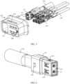
- FIG. 1 is a schematic diagram of a scenario of a connection between devices according to an embodiment of this application
- FIG. 2 is a schematic diagram of a structure of a device according to an embodiment of this application.
- the foregoing devices may be disposed on a vehicle and serve as the vehicle-mounted device. Further, an embodiment of this application may further provide a vehicle.
- the vehicle may include at least two vehicle-mounted devices 500.
- the two vehicle-mounted devices 500 may be connected through a cable 400, and a connection between the vehicle-mounted device 500 and the cable 400 may be implemented by using a connector assembly.
- Vehicle-mounted devices connected through the cable 400 may be a same device, or may be different devices.
- the vehicle-mounted device may include but is not limited to a millimeter wave radar, a video radar, a gateway, a T-BOX (Telematics BOX, Telematics BOX), a GPS (Global Positioning System, Global Positioning System), and an IVI (In-Vehicle Infotainment, In-Vehicle Infotainment).
- one vehicle-mounted device is a lidar
- the other vehicle-mounted device is a vehicle-mounted processing device, for example, a domain controller or the IVI.
- a vehicle-mounted lidar and the domain controller are connected.
- the vehicle-mounted lidar and the domain controller may be cooperatively connected by using the connector assembly, to implement high-speed Ethernet data transmission, low-speed (Controller Area Network, Controller Area Network) CAN signal transmission, driving electrical signal (for example, a power signal) transmission, and another-type signal transmission.
- the connector assembly may include a female connector 100 and a male connector 200.
- the female connector 100 and the male connector 200 may be cooperatively connected to implement an electrical connection and transmit data. It should be understood that one of the female connector 100 and the male connector 200 may be disposed on a device body of the vehicle-mounted device 500, and the other may be disposed on the cable 400.
- an example in which the male connector 200 is disposed on the device body and the female connector 100 is connected to an end of the cable 400 is used to describe specific structures of the male connector 200 and the female connector 100.
- insertion cooperation between the structures of the female connector 100 and the male connector 200, and an electrical connection of a conductive terminal may be implemented by inserting a pin into a jack.
- the pin and the jack may be respectively disposed on the female connector 100 and the male connector 200.
- the jack and the pin may be respectively disposed on the female connector 100 and the male connector 200.
- a structure in which the jack is provided on the female connector 100 and the pin is disposed on the male connector 200 is used as an example.
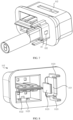
- FIG. 3 is a schematic diagram of a structure of a female connector according to an embodiment of this application.
- An embodiment of this application provides a female connector 100, which may include a first insulating body 11, a first protective housing 12, a first jack 13, and a second jack 14.
- the first insulating body 11 may be disposed in the first protective housing 12.
- the first jack 13 and the second jack 14 are provided on the first insulating body 11.
- the first jack 13 and the second jack 14 are exposed on an opening side of the first protective housing 12.
- the first jack 13 and the second jack 14 are respectively configured to transmit signals with different rates.
- the first jack 13 may be configured to transmit high-speed Ethernet data.
- the second jack 14 may be configured to transmit a low-speed CAN signal and/or a power signal.
- a distance of the spacing is not limited in this embodiment of this application.
- the spacing may be used to facilitate a design of an interference isolation structure between the first jack 13 and the second jack 14, to improve signal transmission quality. This is described in the following embodiments.
- a quantity of the first jacks 13 and a quantity of the second jacks 14 are not specifically limited in this embodiment of this application.
- the first jacks 13 and the second jacks 14 may be arranged from left to right, as shown in FIG. 3 .
- the two first jacks 13 may be arranged from top to bottom in one row.
- the six second jacks 14 may be arranged in two rows and three columns.
- shapes of the first insulating body 11 and the first protective housing 12 are not specifically limited.
- a shape of an opening of the first protective housing 12 may be a rectangle, an ellipse, a polygon, or another shape.
- a shape of the first insulating body 11 exposed on the opening side of the first protective housing 12 may be similar to that of the first protective housing 12.
- the shape of the opening of the first protective housing 12 may be a rounded rectangle. The shape is merely a possible implementation, and does not limit a structure of the first protective housing 12.
- FIG. 4 is a schematic exploded view of a female connector according to an embodiment of this application.
- the first insulating body 11 may include a first support 111 and a second support 112.
- the first jack 13 may be disposed on the first support 111.
- the second jack 14 may be disposed on the second support 112.
- An accommodating cavity 113 may be disposed on the second support 112.
- the first support 111 may be installed in the accommodating cavity 113. There is a spacing between the first support 111 and an inner wall of the accommodating cavity 113.
- the first jack 13 is disposed on the first support 111
- the second jack 14 is disposed on the second support 112
- the first support 111 is installed in the accommodating cavity 113 of the second support 112.
- the first jack 13 and the second jack 14 can be separated, to prevent interference when the first jack 13 and the second jack 14 perform signal transmission and facilitate respective assembly of the first jack 13 and the second jack 14.
- FIG. 5 is a schematic exploded view of a first insulating body according to an embodiment of this application.
- the first jack 13 and the second jack 14 are structures for cooperatively connecting a pin and implementing an electrical connection.
- the first jack 13 may include an opening provided on the first support 111 and a first conductive terminal (not shown in the figure) disposed in the second support 112.
- the first conductive terminal is configured to connect to the first connection cable 132.
- the second jack 14 may include an opening 140 provided on the second support 112 and a second conductive terminal 141 disposed in the second support 112.
- the second conductive terminal 141 is configured to connect to the second connection cable 142.
- the first conductive terminal and the second conductive terminal 141 may be a type of conductive structure like a metal spring plate, to ensure, on the basis of implementing the electrical connection, good electrical contact obtained by inserting a pin into a jack.
- the first connection cable 132 may be a high-speed signal cable
- the second connection cable 142 may be a low-speed signal cable.
- An internal conductive structure and an external protective layer structure of the first connection cable 132 are different from that of the second connection cable 142.
- the female connector 100 may further include a first shielding housing 15, the first shielding housing 15 may cover the first support 111, the first jack 13 is exposed on an opening side of the first shielding housing 15, the first shielding housing 15 may be disposed in the accommodating cavity 113, and there is a spacing between an outer wall of the first shielding housing 15 and the inner wall of the accommodating cavity 113, to further reduce electromagnetic interference between the first jack 13 and the second jack 14.
- the first shielding housing 15 may be a metal piece, for example, may be an aluminum alloy.
- the first shielding housing 15 may cover the first jack 13, to effectively shield electromagnetic interference and improve overall structural strength of the first jack 13 and the first support 111.
- FIG. 6 is a schematic diagram of a structure of a first shielding housing according to an embodiment of this application.
- a spring plate 151 is disposed on an outer surface of the first shielding housing 15.
- the spring plate 151 can play a clamping function, so that after the male connector 200 is connected to the female connector 100, by using the spring plate 151, the first shielding housing 15 can be clamped on a structure that is of the male connector 200 and that is correspondingly inserted between the first shielding housing 15 and the inner wall of the accommodating cavity 113, to ensure a more stable and reliable insertion relationship.
- the spring plate 151 can fill a middle spacing generated by connecting the male connector 200 and the female connector 100, to play a shielding function.
- An opening of the first shielding housing 15 is set to a rectangle, and the spring plate 151 is disposed on each of four side walls that correspond to four sides of the rectangle on the first shielding housing 15.
- the spring plate 151 is disposed on a side wall corresponding to a long side of the rectangle, and at least one spring plate 151 is disposed on a side wall corresponding to a short side of the rectangle.
- more spring plates 151 can be arranged to fill the middle spacing generated by connecting the male connector 200 and the female connector 100, so that the spacing is less than one-quarter wavelength of an electromagnetic wave as far as possible, to achieve a good shielding effect.
- the opening of the first shielding housing 15 is set to the rectangle.
- the rectangle is not strictly limited to a quadrilateral whose four corners are right angles, but may be a chamfered rectangle whose four corners are chamfered or a rounded rectangle whose four corners are rounded.
- the rounded corner and the chamfered corner are arranged at the four corners of the rectangle, which has negligible influence on an overall shape of the rectangle, and is beneficial to technological processing and can prevent stress concentration.
- the opening of the first shielding housing 15 may alternatively be set to a hexagon or another polygon. In comparison, the opening of the first shielding housing 15 is set to the rectangle, which has advantages of simple structure and easy implementation.
- FIG. 7 is a schematic diagram of cooperation between a first shielding housing and a second support according to an embodiment of this application.
- a stop protrusion 152 may be further disposed on the outer surface of the first shielding housing 15.
- the stop protrusion 152 may be disposed on a side that is of the first shielding housing 15 and that is away from the first jack 13.
- the stop protrusion 152 is located outside the accommodating cavity 113, and the stop protrusion 152 may be configured to prevent the first shielding housing 15 and the first support 111 from coming out of the accommodating cavity 113.
- the first shielding housing 15 may include a first section and a second section.
- the first section is close to the opening side of the first protective housing 12.
- a cross-sectional dimension of the first section is less than that of the second section.
- the spring plate 151 is disposed on the first section.
- the stop protrusion 152 is disposed on the second section. It is not difficult to understand that, when the first shielding housing 15 is assembled in the accommodating cavity 113, an outer wall of the first section is spaced from the inner wall of the accommodating cavity 113, and an outer wall of the second end may be in interference fit with the inner wall of the accommodating cavity 113.
- FIG. 8 is a schematic diagram of a structure of a second support according to an embodiment of this application.
- FIG. 9 is a schematic diagram of a structure of a first protective housing according to an embodiment of this application.
- FIG. 10 is a schematic diagram of a structure of a first protective housing from another angle according to an embodiment of this application. Refer to FIG. 8 to FIG. 10 .
- the second support 112 may be installed in the first protective housing 12, and the first protective housing 12 and the second support 112 may be connected in a manner of abutting, clamping, or the like, to jointly limit positions of the first shielding housing 15 and the second conductive terminal 141.
- a first limiting cavity 121 may be disposed in the first protective housing 12.
- the first limiting cavity 121 may be disposed opposite to the accommodating cavity 113.
- the first shielding housing 15 may be installed in the first limiting cavity 121.
- the first limiting cavity 121 is a cavity that may also be provided with a rectangular opening.
- the first shielding housing 15 may be in interference fit with an inner side wall of the first limiting cavity 121.
- the first limiting cavity 121 may prevent the first shielding housing 15 from moving inward after being subject to an action force generated by inserting a pin into the first jack 13.
- a second limiting cavity 123 may be further disposed in the first protective housing 12, and the second conductive terminal 141 may be installed in the second limiting cavity 123.
- the second support 112 covers the second limiting cavity 123, and the second conductive terminal 141 is clamped in the second limiting cavity 123 and is located in the second support 112.
- the second limiting cavity 123 can prevent the second conductive terminal 141 from moving inward after being subject to an action force generated by inserting the pin into the second jack 14.
- a first limiting slot 122 may be disposed on the inner side wall of the first limiting cavity 121.
- a first limiting boss 1121 may be disposed on the second support 112. The first limiting boss 1121 is disposed on a side that faces the first limiting cavity 121 and that is of the second support 112, and is located on a peripheral side of the accommodating cavity 113. The first limiting boss 1121 may be clamped in the first limiting slot 122.
- first limiting slots 122 there may be three first limiting slots 122 that are respectively located on three inner side walls of the first limiting cavity 121. It should be understood that the first limiting slot 122 is not disposed on the remaining side wall, to avoid the stop protrusion 152.
- the three first limiting bosses 1121 and the first limiting slots 122 are disposed in a one-to-one correspondence.
- the first limiting bosses 1121 are clamped in the first limiting slot 122 to prevent the second support 112 from moving inward after being subject to a force, and limit a position of the first shielding housing 15 to prevent poor electrical contact caused by moving the first jack 13 up and down.
- a buckle and the inner side wall of the first limiting cavity 121 may form the first limiting slot 122.
- the buckle has specific elasticity and deformation, and can be configured to clamp the first shielding housing 115.
- the second limiting cavity 123 may include a second limiting slot 124.
- a second limiting boss 1122 is disposed on the second support 112.
- the second limiting boss 1122 is disposed on a side that faces the second limiting cavity 123 and that is of the second support 112.
- the second limiting boss 1122 is clamped in the second limiting slot 124.
- another cavity configured to accommodate the second limiting cavity 123 may be disposed on the second support 112.
- the cavity may be divided into an upper part and a lower part.
- the second limiting boss 1122 is disposed between the upper part and the lower part of the cavity.
- the second limiting slot 124 may be disposed between two adjacent sub-cavities 1231.
- the second limiting boss 1122 may be clamped in the second limiting slot 124 to prevent the second support 112 from moving inward after being subject to a force, and limit a position of the second conductive terminal 141 to prevent poor electrical contact caused by moving the second conductive terminal 141 up and down.
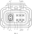
- FIG. 11 is a front view of a female connector according to an embodiment of this application.
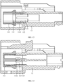
- FIG. 12 is a cross sectional view of FIG. 11 at A-A.
- structures of the first jack 13, the first support 111, and the first shielding housing 15 are omitted in FIG. 12 .
- FIG. 13 is a cross sectional view of FIG. 11 at B-B.
- a structure of the second conductive terminal 141 is omitted in FIG. 13 .
- the second support 112 and the first protective housing 12 are assembled, the second support 112 covers the second limiting cavity 123, and the second limiting boss 1122 is clamped in the second limiting slot 124.
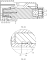
- FIG. 14 is a cross sectional view of FIG. 11 at C-C.
- FIG. 15 is an enlarged view of a circle portion of FIG. 14 .
- a protrusion 1123 may be disposed on an inner side wall of the second support 112.
- a first groove 125 and a second groove 126 are disposed on an outer side wall of the second limiting cavity 123.
- the first groove 125 and the second groove 126 are arranged in an extension direction of the second conductive terminal.
- the first groove 125 is located on a side close to the second jack 14.
- the protrusion 1123 is configured to be clamped in the first groove 125 or the second groove 126.
- the two or more first grooves 125 may be arranged in a row.
- the two or more second grooves 126 may be arranged in a row.
- an assembling process of the female connector 100 may be as follows: First, the first shielding housing 15 and the second conductive terminal 141 are installed in the first protective housing 12, and then the second support 112 is pushed into the first protective housing 12 from an opening of the first protective housing 12.
- the protrusion 1123 on the second support 112 may be clamped in the first groove 125, which is equivalent to pre-assembly, and can ensure that the second support 112 and the first protective housing 12 are accurately positioned before assembly.
- an inward force is continuously applied to the second support 112, and the second support 112 moves inward until the protrusion 1123 is clamped in the second groove 126, so that the second support 112 is assembled in place.
- the second support 112 and the first protective housing 12 can be reliably fastened.
- the first groove 125 and the second groove 126 may be disposed, to facilitate assembly of the second support 112 and the first protective housing 12, and reduce assembly costs.
- a disassembly groove 114 may be further disposed on the first insulating body 11.
- the disassembly groove 114 is disposed on an outer side wall surface of the first insulating body 11, and the outer side wall surface is adjacent to a wall surface on which the first jack 13 and the second jack 14 are exposed.
- a disassembly tool may be clamped in the disassembly groove 114, to disassemble the second support 112 from the first protective housing 12.
- the disassembly groove 114 is disposed, so that corresponding avoidance processing does not need to be performed on the male connector 200, and design costs can be reduced.
- a guiding groove 127 may also be disposed on an inner side wall of the first protective housing 12, and the guiding groove 127 extends inward from the opening side of the first protective housing 12.
- the two guiding grooves 127 are respectively disposed on two opposite inner side walls of the first protective housing 12, and are configured to cooperate with a structure like a guiding rib on the male connector 200 to play a guiding function, to facilitate a connection between the female connector 100 and the male connector 200.
- a first jack configured to transmit high-speed Ethernet data and a second jack configured to transmit a low-speed CAN signal and/or a power supply can be integrated into the first protective housing, to reduce a volume of the connector and plug-in and out durability.
- electromagnetic interference between the first jack and the second jack can be reduced by disposing the first shielding housing.
- structures such as a boss and a clamping slot that cooperate with each other on a first support body and the first protective housing can limit positions of the first jack and the second jack in design, to prevent poor electrical contact caused by displacement.
- FIG. 16 is a schematic diagram of a structure of a male connector according to an embodiment of this application.
- An embodiment of this application provides the male connector 200, which may include a second insulating body 21, a second protective housing 22, a first pin 23, and a second pin 24.
- the first pin 23 and the second pin 24 may be convexly disposed on the second insulating body 21.
- the second protective housing 22 is connected to the second insulating body 21.
- the second protective housing 22 is disposed around the first pin 23 and the second pin 24.
- the first pin 23 and the second pin 24 are exposed on an opening side of the second protective housing 22. There is a spacing between the first pin 23 and the second pin 24.
- the first pin 23 and the second pin 24 are respectively configured to transmit signals with different rates.
- the first pin 23 may be configured to transmit the high-speed Ethernet data.
- the second pin 24 may be configured to transmit the low-speed CAN signal and/or the power signal. There is a spacing between the first pin 23 and the second pin 24, to reduce mutual influence between signals. Compared with a manner in which each of the first pin 23 and the second pin 24 is disposed in one protective housing, a manner in which the first pin 23 and the second pin 24 are integrated into the second protective housing 22 can reduce a volume of the male connector 200, facilitate a connection, and improve installation efficiency.
- shapes of the second insulating body 21 and the second protective housing 22 are not specifically limited.
- An opening of the second protective housing 22 may be a rectangle, an ellipse, a polygon, or another shape.
- a shape of the second insulating body 21 exposed on the opening side of the second protective housing 22 may be similar to that of the second protective housing 22.
- the opening of the second protective housing 22 may be a rounded rectangle.
- the shape is merely a possible implementation, and does not limit a structure of the second protective housing 22.
- the first pin 23 is configured to be inserted into the first jack 13 and conduct a power connection, to transmit the high-speed Ethernet data.
- the second pin 24 is configured to be inserted into the second jack 14 and conduct a power connection, to transmit the low-speed CAN signal and the power signal.
- the first pin 23 and the second pin 24 are disposed corresponding to the first jack 13 and the second jack 14 in quantity and arrangement. Details are not described herein again.
- the second protective housing 22 When the female connector 100 and the male connector 200 are cooperatively connected, the second protective housing 22 is inserted into accommodating space between the first protective housing 12 and the first insulating body 11.
- the second protective housing 22 and the first protective housing 12 are similar in shape, and both may be set to rounded rectangles.
- a guiding rib 221 may be disposed on an outer side wall of the second protective housing 22.
- the guiding rib 221 extends in a direction close to the second insulating body 21 from the opening side of the second protective housing 22.
- An extension direction of the guiding rib 221 is consistent with an extension direction of the first pin 23 and the second pin 24.
- the guiding rib 221 is configured to be clamped in the guiding groove 127 and move in the guiding groove 127, so that the female connector 100 can move along a fixed position when being inserted into the male connector 200.
- the guiding function facilitates smooth insertion cooperation between a pin and a jack.
- the male connector 200 may further include a second shielding housing 25.
- the second shielding housing 25 may be disposed around the first pin 23.
- the first pin 23 is exposed on an opening side of the second shielding housing 25.
- the second shielding housing 25 may be a metal piece, for example, may be an aluminum alloy.
- the second shielding housing 25 may cover the first pin 23, to effectively shield electromagnetic interference.
- the second shielding housing 25 is inserted between the first shielding housing 15 and the accommodating cavity 113.
- the spring plate 151 is disposed on the outer surface of the first shielding housing 15, the spring plate 151 is clamped on an inner wall of the second shielding housing 25.
- FIG. 17 is a schematic diagram of another structure of a male connector according to an embodiment of this application.
- the male connector 200 further includes a mounting plate 28.
- the mounting plate 28 is connected to a periphery of the second insulating body 21.
- a mounting hole 281 is disposed on the mounting plate 28.
- the mounting hole 281 is configured to mount a threaded fastener to fasten the male connector 200 to a to-be-installed device.
- the to-be-installed device may be a vehicle-mounted device, for example, a vehicle-mounted lidar or a domain controller.
- the mounting holes 281 can be disposed at four corners of the mounting plate 28, to better fasten the mounting plate 28 to the to-be-installed device without loosening.
- FIG. 18 is a schematic exploded view of a male connector according to an embodiment of this application.
- FIG. 19 is a schematic diagram of a structure of a male connector from another angle according to an embodiment of this application.
- the male connector 200 may further include a circuit board 26.
- the circuit board 26 may be disposed on a side that is far away from the second protective housing 22 and that is of the second insulating body 21.
- the first pin 23 and the second pin 24 penetrate in through holes of the second insulating body 21 and are fastened to the circuit board 26.
- the first pin 23 and the second pin 24 may penetrate the second insulating body 21 and be soldered on the circuit board 26, to implement an electrical connection to the circuit board 26 while being reliably fastened.
- the second shielding housing 25 may penetrate in a through hole of the second insulating body 21 and be fastened to the circuit board 26; or the second shielding housing 25 may be soldered on the circuit board 26 or clamped and fastened to the circuit board 26 by using a bending structure. In this case, the second shielding housing 25 may cover an entire length of the first pin 23, to achieve a good shielding effect.
- Three positioning pins 27 are further disposed on the second insulating body 21, and are arranged in a triangle to form a stable triangle structure.
- Three positioning holes 261 are disposed on the circuit board 26.
- the positioning pin 27 penetrates in the positioning hole 261.
- the circuit board 26 can be pre-positioned through cooperation between the positioning pin 27 and the positioning hole 261, to prevent a pin damage or a soldering failure caused by moving the circuit board 26 in a soldering process. It is not difficult to understand that there may be at least three positioning pins 27 to form the triangular structure.
- a quantity of positioning pins may be increased, to increase stability or replace the triangular structure.
- a first pin configured to transmit the high-speed Ethernet data and the second pin configured to transmit the low-speed CAN signal and/or the power signal can be integrated into the second protective housing, to reduce a volume of the connector, an area of the circuit board, and plug-in and out durability.
- electromagnetic interference between the first pin and the second pin can be reduced by disposing the second shielding housing.
- An embodiment of this application further provides a connector assembly.
- the connector assembly includes the female connector 100 and the male connector 200 provided in the foregoing embodiments. Specific structures of the female connector 100 and the male connector 200 are not described herein again.
- FIG. 20 is a front view of a male connector according to an embodiment of this application.
- FIG. 21 is a schematic diagram of cooperation between a female connector and a male connector according to an embodiment of this application. Refer to FIG. 11 , FIG. 20 , and FIG. 21 .
- the second protective housing 22 is inserted into the accommodating space between the first protective housing 12 and the first insulating body 11.
- the second shielding housing 25 is inserted between the first shielding housing 15 and the accommodating cavity 113.
- the spring plate 151 is clamped on the inner wall of the second shielding housing 25.
- the guiding rib 221 is clamped in the guiding groove 127.
- a high-speed transmission cable is configured to transmit the high-speed Ethernet data
- a low-speed transmission cable is configured to transmit the low-speed CAN signal and/or the power signal.
- a high-speed connector configured to transmit a high-speed signal and a low-speed connector configured to transmit a low-speed signal can be combined, to reduce a volume of the connector, and simultaneously transmit the high-speed signal and the low-speed signal by wiring only once. Convenience and efficiency of a user operation can be improved by reducing plug-in and out durability of the connector. In addition, manufacturing costs of the connector can be greatly reduced by combining the two connectors.
- an embodiment of this application further provides a vehicle-mounted device.
- the female connector or the male connector provided in embodiments of this application may be disposed on the vehicle-mounted device.
- An embodiment of this application further provides a cable.
- the female connector or the male connector provided in embodiments of this application may be disposed on the cable.
- the male connector 200 may be disposed on the vehicle-mounted device 500.
- the female connector 100 may be disposed on the cable 400.
- the male connector 200 and the female connector 100 may be cooperatively connected to transmit a signal between the cable 400 and the vehicle-mounted device 500.
- the female connector 100 because cooperative structures between a jack, a conductive terminal, and a housing inside the female connector are more complex than that of the male connector 200, the female connector 100 is connected to the cable 400, so that the female connector 100 is easily disassembled and maintained after being damaged, and the female connector may be directly replaced with a new product in the event of a serious damage. Therefore, costs are low.
- the male connector 200 has a simple internal structure and is not easily damaged.
- the male connector 200 can be installed on the vehicle-mounted device 500, to reduce a damage probability and maintenance costs of the vehicle-mounted device 400.
- a user holds the cable 400 and inserts the female connector 100 with a jack into the male connector 200 with a pin, it is difficult for the user to touch the live pin. This provides high security.
- An embodiment of this application may further provide a terminal.
- the terminal may include the female connector or the male connector provided in embodiments of this application.
- the terminal may be a device, for example, a vehicle, a ship, an aircraft, or a spacecraft.
- a connector assembly used in each of these terminals may be a power connector, a high-speed signal connector, an aviation connector, an optical fiber connector, or the like.
- the connector provided in embodiments of this application that combines the high-speed connector and the low-speed connector can be used in the terminal, to reduce plug-in and out durability and facilitate a miniaturized design of the terminal.
Landscapes
- Details Of Connecting Devices For Male And Female Coupling (AREA)
- Connector Housings Or Holding Contact Members (AREA)
Applications Claiming Priority (2)
| Application Number | Priority Date | Filing Date | Title |
|---|---|---|---|
| CN202111017392.9A CN115732978A (zh) | 2021-08-31 | 2021-08-31 | 母连接器、公连接器、连接器组件和车载设备 |
| PCT/CN2022/113553 WO2023030039A1 (zh) | 2021-08-31 | 2022-08-19 | 母连接器、公连接器、连接器组件和车载设备 |
Publications (2)
| Publication Number | Publication Date |
|---|---|
| EP4383473A1 true EP4383473A1 (de) | 2024-06-12 |
| EP4383473A4 EP4383473A4 (de) | 2024-11-20 |
Family
ID=85291810
Family Applications (1)
| Application Number | Title | Priority Date | Filing Date |
|---|---|---|---|
| EP22863178.4A Pending EP4383473A4 (de) | 2021-08-31 | 2022-08-19 | Buchsenstecker, stecker, steckeranordnung und fahrzeugmontierte vorrichtung |
Country Status (5)
| Country | Link |
|---|---|
| US (1) | US20240258753A1 (de) |
| EP (1) | EP4383473A4 (de) |
| JP (1) | JP7764583B2 (de) |
| CN (1) | CN115732978A (de) |
| WO (1) | WO2023030039A1 (de) |
Families Citing this family (6)
| Publication number | Priority date | Publication date | Assignee | Title |
|---|---|---|---|---|
| US12573792B2 (en) * | 2022-09-28 | 2026-03-10 | Microsoft Technology Licensing, Llc | Retractable connector |
| CN116865019B (zh) * | 2023-08-07 | 2025-10-14 | 珠海格力电器股份有限公司 | 引脚结构、连接器件、连接方法及拆卸方法 |
| CN120237471A (zh) * | 2023-12-29 | 2025-07-01 | 华为技术有限公司 | 一种高速连接器 |
| CN118174110B (zh) * | 2024-05-09 | 2024-07-09 | 成都广润恒创智能科技有限公司 | 一种组装机 |
| CN119581946B (zh) * | 2024-07-25 | 2025-10-17 | 济南华云科雷防雷科技有限责任公司 | 一种智能应急电源连接器及其检测方法 |
| CN119890838B (zh) * | 2025-03-28 | 2025-05-23 | 深圳市国信达科技股份有限公司 | 一种高速背板连接器 |
Family Cites Families (11)
| Publication number | Priority date | Publication date | Assignee | Title |
|---|---|---|---|---|
| US6183299B1 (en) * | 1998-05-29 | 2001-02-06 | The Whitaker Corporation | Automotive cellular phone connector assembly |
| US6383031B1 (en) * | 2000-03-31 | 2002-05-07 | Tektronix, Inc. | Keyed electronic interconnect device for high speed signal and data transmission |
| US7682191B2 (en) * | 2007-08-10 | 2010-03-23 | Yazaki Corporation | Connector |
| EP2345112B1 (de) * | 2008-10-24 | 2016-11-30 | Molex, LLC | Rundsteckverbinder mit leistungsstrom und steuerstromkontaktanordnung |
| CN203277815U (zh) * | 2013-05-20 | 2013-11-06 | 深圳市锐明视讯技术有限公司 | 车载连接器 |
| CN110635304B (zh) * | 2014-02-06 | 2022-04-12 | 安费诺富加宜(亚洲)私人有限公司 | 连接器组件 |
| DE102015119087A1 (de) * | 2015-11-06 | 2017-05-11 | Beckhoff Automation Gmbh | Hybrid-Steckverbinder |
| US9667002B1 (en) * | 2016-10-24 | 2017-05-30 | Te Connectivity Corporation | Connector assembly with an unshielded twisted pair circuit |
| KR102633954B1 (ko) * | 2018-12-12 | 2024-02-05 | 현대자동차주식회사 | 통합형 다극 커넥터 |
| JP7102381B2 (ja) * | 2019-10-07 | 2022-07-19 | 矢崎総業株式会社 | コネクタ構造およびハウジング |
| CN216672089U (zh) * | 2021-12-31 | 2022-06-03 | 泰科电子科技(苏州工业园区)有限公司 | 混合式连接器壳体、混合式连接器和连接器组件 |
-
2021
- 2021-08-31 CN CN202111017392.9A patent/CN115732978A/zh active Pending
-
2022
- 2022-08-19 JP JP2024513465A patent/JP7764583B2/ja active Active
- 2022-08-19 EP EP22863178.4A patent/EP4383473A4/de active Pending
- 2022-08-19 WO PCT/CN2022/113553 patent/WO2023030039A1/zh not_active Ceased
-
2024
- 2024-02-29 US US18/591,674 patent/US20240258753A1/en active Pending
Also Published As
| Publication number | Publication date |
|---|---|
| US20240258753A1 (en) | 2024-08-01 |
| JP7764583B2 (ja) | 2025-11-05 |
| JP2024532442A (ja) | 2024-09-05 |
| EP4383473A4 (de) | 2024-11-20 |
| CN115732978A (zh) | 2023-03-03 |
| WO2023030039A1 (zh) | 2023-03-09 |
Similar Documents
| Publication | Publication Date | Title |
|---|---|---|
| US20240258753A1 (en) | Female Connector, Male Connector, Connector Assembly, and Vehicle-Mounted Device | |
| US11011874B2 (en) | Connector and connector assembly | |
| US11616314B2 (en) | Electrical connector assembly with improved shielding effect and easy installation | |
| US8672707B2 (en) | Connector assembly configured to align communication connectors during a mating operation | |
| CN109038054B (zh) | 包括具有传热翅片的冷却通道的可插拔模块 | |
| EP3958410A1 (de) | Signalverbinder und endgerät | |
| US8292669B2 (en) | Electrical connector having contact modules | |
| US7824197B1 (en) | Modular connector system | |
| US8537558B2 (en) | Electronic module with improved latch mechanism | |
| US7329154B2 (en) | Electrical connector having terminals arranged with narrow pitch | |
| US10104793B2 (en) | EMI shielding for pluggable modules and connector assemblies | |
| US6206725B1 (en) | Connector assembly | |
| US10243305B1 (en) | Electrical connector assembly | |
| US9666997B1 (en) | Gasket plate for a receptacle assembly of a communication system | |
| US11695241B2 (en) | Electrical connector assembly with improved shielding effect and locking structure | |
| US6623301B2 (en) | Plug connector for electronic devices | |
| CN217545045U (zh) | 母连接器、公连接器、连接器组件、车载设备、线缆和终端 | |
| US20180205184A1 (en) | Receptacle cage member having locating features | |
| US12562533B2 (en) | Protective cage assembly, receptacle connector and connector assembly with improved light guide pipe | |
| US20060030172A1 (en) | Cable connector assembly having improved mating port | |
| US20260088573A1 (en) | Connector and assembly thereof with foolproof structure | |
| EP4336674A1 (de) | Verbinder und elektronische vorrichtung | |
| US6923679B1 (en) | Cable assembly floatably mounted on a panel | |
| EP4312316B1 (de) | Subverbinder, verbinder und verbinderanordnung | |
| CN103457056B (zh) | 使用直角、板安装的连接器的连接器系统 |
Legal Events
| Date | Code | Title | Description |
|---|---|---|---|
| STAA | Information on the status of an ep patent application or granted ep patent |
Free format text: STATUS: THE INTERNATIONAL PUBLICATION HAS BEEN MADE |
|
| PUAI | Public reference made under article 153(3) epc to a published international application that has entered the european phase |
Free format text: ORIGINAL CODE: 0009012 |
|
| STAA | Information on the status of an ep patent application or granted ep patent |
Free format text: STATUS: REQUEST FOR EXAMINATION WAS MADE |
|
| 17P | Request for examination filed |
Effective date: 20240305 |
|
| AK | Designated contracting states |
Kind code of ref document: A1 Designated state(s): AL AT BE BG CH CY CZ DE DK EE ES FI FR GB GR HR HU IE IS IT LI LT LU LV MC MK MT NL NO PL PT RO RS SE SI SK SM TR |
|
| A4 | Supplementary search report drawn up and despatched |
Effective date: 20241022 |
|
| RIC1 | Information provided on ipc code assigned before grant |
Ipc: H01R 13/6596 20110101ALI20241016BHEP Ipc: H01R 13/6581 20110101ALI20241016BHEP Ipc: H01R 13/52 20060101ALI20241016BHEP Ipc: H01R 13/648 20060101ALI20241016BHEP Ipc: H01R 24/00 20110101ALI20241016BHEP Ipc: H01R 13/02 20060101ALI20241016BHEP Ipc: H01R 13/40 20060101ALI20241016BHEP Ipc: H01R 13/502 20060101ALI20241016BHEP Ipc: H01R 13/516 20060101AFI20241016BHEP |
|
| DAV | Request for validation of the european patent (deleted) | ||
| DAX | Request for extension of the european patent (deleted) | ||
| RAP1 | Party data changed (applicant data changed or rights of an application transferred) |
Owner name: SHENZHEN YINWANG INTELLIGENTTECHNOLOGIES CO., LTD. |