EP4383544A1 - Weicher schaltkreis, leiterplattenanordnung und schaltnetzteil - Google Patents
Weicher schaltkreis, leiterplattenanordnung und schaltnetzteil Download PDFInfo
- Publication number
- EP4383544A1 EP4383544A1 EP21952596.1A EP21952596A EP4383544A1 EP 4383544 A1 EP4383544 A1 EP 4383544A1 EP 21952596 A EP21952596 A EP 21952596A EP 4383544 A1 EP4383544 A1 EP 4383544A1
- Authority
- EP
- European Patent Office
- Prior art keywords
- switch transistor
- auxiliary
- switch
- transistor
- turn
- Prior art date
- Legal status (The legal status is an assumption and is not a legal conclusion. Google has not performed a legal analysis and makes no representation as to the accuracy of the status listed.)
- Pending
Links
Images

Classifications
-
- H—ELECTRICITY
- H02—GENERATION; CONVERSION OR DISTRIBUTION OF ELECTRIC POWER
- H02M—APPARATUS FOR CONVERSION BETWEEN AC AND AC, BETWEEN AC AND DC, OR BETWEEN DC AND DC, AND FOR USE WITH MAINS OR SIMILAR POWER SUPPLY SYSTEMS; CONVERSION OF DC OR AC INPUT POWER INTO SURGE OUTPUT POWER; CONTROL OR REGULATION THEREOF
- H02M1/00—Details of apparatus for conversion
- H02M1/0048—Circuits or arrangements for reducing losses
- H02M1/0054—Transistor switching losses
- H02M1/0058—Transistor switching losses by employing soft switching techniques, i.e. commutation of transistors when applied voltage is zero or when current flow is zero
-
- H—ELECTRICITY
- H02—GENERATION; CONVERSION OR DISTRIBUTION OF ELECTRIC POWER
- H02M—APPARATUS FOR CONVERSION BETWEEN AC AND AC, BETWEEN AC AND DC, OR BETWEEN DC AND DC, AND FOR USE WITH MAINS OR SIMILAR POWER SUPPLY SYSTEMS; CONVERSION OF DC OR AC INPUT POWER INTO SURGE OUTPUT POWER; CONTROL OR REGULATION THEREOF
- H02M1/00—Details of apparatus for conversion
- H02M1/0064—Magnetic structures combining different functions, e.g. storage, filtering or transformation
-
- H—ELECTRICITY
- H02—GENERATION; CONVERSION OR DISTRIBUTION OF ELECTRIC POWER
- H02M—APPARATUS FOR CONVERSION BETWEEN AC AND AC, BETWEEN AC AND DC, OR BETWEEN DC AND DC, AND FOR USE WITH MAINS OR SIMILAR POWER SUPPLY SYSTEMS; CONVERSION OF DC OR AC INPUT POWER INTO SURGE OUTPUT POWER; CONTROL OR REGULATION THEREOF
- H02M3/00—Conversion of DC power input into DC power output
- H02M3/02—Conversion of DC power input into DC power output without intermediate conversion into AC
- H02M3/04—Conversion of DC power input into DC power output without intermediate conversion into AC by static converters
- H02M3/10—Conversion of DC power input into DC power output without intermediate conversion into AC by static converters using discharge tubes with control electrode or semiconductor devices with control electrode
- H02M3/145—Conversion of DC power input into DC power output without intermediate conversion into AC by static converters using discharge tubes with control electrode or semiconductor devices with control electrode using devices of a triode or transistor type requiring continuous application of a control signal
- H02M3/155—Conversion of DC power input into DC power output without intermediate conversion into AC by static converters using discharge tubes with control electrode or semiconductor devices with control electrode using devices of a triode or transistor type requiring continuous application of a control signal using semiconductor devices only
- H02M3/156—Conversion of DC power input into DC power output without intermediate conversion into AC by static converters using discharge tubes with control electrode or semiconductor devices with control electrode using devices of a triode or transistor type requiring continuous application of a control signal using semiconductor devices only with automatic control of output voltage or current, e.g. switching regulators
- H02M3/158—Conversion of DC power input into DC power output without intermediate conversion into AC by static converters using discharge tubes with control electrode or semiconductor devices with control electrode using devices of a triode or transistor type requiring continuous application of a control signal using semiconductor devices only with automatic control of output voltage or current, e.g. switching regulators including plural semiconductor devices as final control devices for a single load
- H02M3/1582—Buck-boost converters
-
- H—ELECTRICITY
- H03—ELECTRONIC CIRCUITRY
- H03K—PULSE TECHNIQUE
- H03K17/00—Electronic switching or gating, i.e. not by contact-making and –breaking
- H03K17/13—Modifications for switching at zero crossing
- H03K17/133—Modifications for switching at zero crossing in field-effect transistor switches
-
- H—ELECTRICITY
- H03—ELECTRONIC CIRCUITRY
- H03K—PULSE TECHNIQUE
- H03K17/00—Electronic switching or gating, i.e. not by contact-making and –breaking
- H03K17/16—Modifications for eliminating interference voltages or currents
- H03K17/161—Modifications for eliminating interference voltages or currents in field-effect transistor switches
- H03K17/165—Modifications for eliminating interference voltages or currents in field-effect transistor switches by feedback from the output circuit to the control circuit
- H03K17/166—Soft switching
- H03K17/167—Soft switching using parallel switching arrangements
-
- H—ELECTRICITY
- H03—ELECTRONIC CIRCUITRY
- H03K—PULSE TECHNIQUE
- H03K2217/00—Indexing scheme related to electronic switching or gating, i.e. not by contact-making or -breaking covered by H03K17/00
- H03K2217/0036—Means reducing energy consumption
-
- Y—GENERAL TAGGING OF NEW TECHNOLOGICAL DEVELOPMENTS; GENERAL TAGGING OF CROSS-SECTIONAL TECHNOLOGIES SPANNING OVER SEVERAL SECTIONS OF THE IPC; TECHNICAL SUBJECTS COVERED BY FORMER USPC CROSS-REFERENCE ART COLLECTIONS [XRACs] AND DIGESTS
- Y02—TECHNOLOGIES OR APPLICATIONS FOR MITIGATION OR ADAPTATION AGAINST CLIMATE CHANGE
- Y02B—CLIMATE CHANGE MITIGATION TECHNOLOGIES RELATED TO BUILDINGS, e.g. HOUSING, HOUSE APPLIANCES OR RELATED END-USER APPLICATIONS
- Y02B70/00—Technologies for an efficient end-user side electric power management and consumption
- Y02B70/10—Technologies improving the efficiency by using switched-mode power supplies [SMPS], i.e. efficient power electronics conversion e.g. power factor correction or reduction of losses in power supplies or efficient standby modes
Definitions
- the present disclosure relates to the field of circuit design, and in particular, to a soft switch circuit, a circuit board assembly, and a switch power supply.
- the switch power supply has advantages in terms of the volume and the characteristic of high conversion efficiency when only working in a switch state due to its high frequency, and thus is most widely applied in the current electronic technology field. With the continuous increase in demand for power of devices, people's requirements for power density and efficiency of the switch power supply are also continuously rising.
- a traditional switch power supply includes a switch circuit.
- the switch circuit usually includes a plurality of switch devices. During a switching operation, each of the switch devices needs to bear a voltage and a current at the same time, and a parasitic capacitor in the switch device is charged and discharged.
- the switching loss of a switch device is related to a product of a current flowing through the switch device and a voltage on the switch device, the switching loss of the switch device may be generated during each switching operation. If the switching frequency of a switch device in the switch circuit is continuously increased, the ratio between a total switching loss generated by all the switch devices in the switch circuit and an input power of the switch circuit is gradually increased, that is, the efficiency of the switch circuit is reduced. Hence, the switching loss of the switch device becomes a main factor for preventing the switching frequency of the switch device in the switch circuit from being further increased, and thus preventing the volume of the switch power supply applying the switch circuit from being further reduced.
- the embodiments of the present disclosure provide a soft switch circuit.
- the soft switch circuit includes a power supply, a first switch transistor, a second switch transistor, a third switch transistor, a fourth switch transistor, a capacitor, a main inductor, an auxiliary switch transistor, an auxiliary inductor, and a control unit; wherein a negative electrode of the power supply is grounded, a positive electrode of the power supply is connected to a first end of the first switch transistor, a second end of the first switch transistor is connected to a first end of the second switch transistor and a first end of the main inductor respectively, a second end of the second switch transistor is grounded, a second end of the main inductor is connected to a first end of the third switch transistor and a second end of the fourth switch transistor respectively, a second end of the third switch transistor is grounded, a first end of the fourth switch transistor is connected to a first end of the capacitor, and a second end of the capacitor is grounded, wherein a negative electrode of a body diode of each switch transistor
- the embodiments of the present disclosure further provide a circuit board assembly including the soft switch circuit described above.
- the embodiments of the present disclosure further provide a switch power supply including the circuit board assembly described above.
- the main objective of the embodiments of the present disclosure is to provide a soft switch circuit, a circuit board assembly, and a switch power supply, which provides a soft switch circuit capable of effectively reducing the switching loss of a switch device.
- a control unit turns on an auxiliary switch transistor, so that an auxiliary inductor and a main inductor are connected in parallel to form an equivalent inductor, where the inductance value of the equivalent inductor is less than the inductance value of the auxiliary inductor and the main inductor, and the inductance value of the equivalent inductor is smaller, so that the current on the main inductor can quickly decease to 0, thereby implementing zero-voltage turn-on of each switch transistor, further reducing the switching loss of each switch transistor.
- An embodiment of the present disclosure relates to a soft switch circuit.
- the soft switch circuit is provided in a switch power supply.
- the switching loss of each switch transistor in the switch power supply is generated when the switch transistor is turned on or turned off.
- the switch transistor is, for example, an MOS transistor.
- the parasitic output capacitor of the MOS transistor consumes energy when the MOS transistor is turned on, which is the main source of the switching loss of the switch power supply.
- the soft switch circuit in the present disclosure is used for releasing and recycling the energy on the parasitic output capacitor of the MOS transistor before the MOS transistor is turned on, so as to implement zero-voltage turn-on of the MOS transistor, and reduce the switching loss of the entire switch power supply, and then the switching frequency of the MOS transistor can be increased to further reduce the volume of the switch power supply applying the switch circuit.
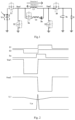
- the soft switch circuit includes a power supply 1, a first switch transistor S1, a second switch transistor S2, a third switch transistor S3, a fourth switch transistor S4, a capacitor C, a main inductor L1, an auxiliary switch transistor Sa, an auxiliary inductor La, and a control unit (not shown in the figure).
- the circuit connection structure is as follows: a negative electrode of the power supply 1 is grounded, a positive electrode of the power supply 1 is connected to a first end of the first switch transistor S1, a second end of the first switch transistor S1 is connected to a first end of the second switch transistor S2 and a first end of the main inductor L1 respectively, a second end of the second switch transistor S2 is grounded, a second end of the main inductor L1 is connected to a first end of the third switch transistor S3 and a second end of the fourth switch transistor S4 respectively, a second end of the third switch transistor S3 is grounded, a first end of the fourth switch transistor S4 is connected to a first end of the capacitor C, and a second end of the capacitor C is grounded, wherein a negative electrode of a body diode of each switch transistor serves as the first end of each switch transistor, and a positive electrode of a body diode of each switch transistor serves as the second end of each switch transistor; the auxiliary switch transistor Sa and the auxiliary inductor La are
- S1, S2, S3 and S4 can all be MOS transistors.
- Fig. 1 shows an example in which S1, S2, S3 and S4 are all MOS transistors.
- the auxiliary switch transistor Sa can be an MOS transistor, and the control unit is specifically connected to a gate of each MOS transistor to control the conduction or disconnection between the first end (drain/source) and the second end (source/drain) of various MOS transistors.
- the control unit may control the first switch transistor S1 and the second switch transistor S2 to be turned on complementarily, and control the third switch transistor S3 and the fourth switch transistor S4 to be turned on complementarily; or, when the current IL1 of the main inductor L1 is positive, that is, when IL1 only flows from the first end to the second end of the main inductor L1, the second switch transistor S2 and the fourth switch transistor S4 may be configured to be diodes; and when the current of the main inductor is negative, that is, when IL1 only flows from the second end to the first end of the main inductor L1, the first switch transistor S1 and the third switch transistor S3 may be configured to be diodes.
- the control unit When the current IL1 of the main inductor L1 is positive, the control unit turns on the auxiliary switch transistor Sa before the first switch transistor S1 and the third switch transistor S3 are turned on; and when the current IL1 of the main inductor L1 is negative, the control unit turns on the auxiliary switch transistor Sa before the second switch transistor S2 and the fourth switch transistor S4 are turned on.
- a soft switch circuit capable of effectively reducing the switching loss of a switch device.
- a control unit turns on an auxiliary switch transistor, so that an auxiliary inductor and a main inductor are connected in parallel to form an equivalent inductor, where the inductance value of the equivalent inductor is less than the inductance value of the auxiliary inductor and the main inductor, and the inductance value of the equivalent inductor is smaller, so that the current on the main inductor can quickly decrease to 0, thereby implementing zero-voltage turn-on of each switch transistor, further reducing the switching loss of each switch transistor.
- the first switch transistor S1, the second switch transistor S2, and the main inductor L1 form a BUCK circuit
- the third switch transistor S3, the fourth switch transistor S4, and the main inductor L1 form a BOOST circuit.
- the control unit may control the first switch transistor S1 and the second switch transistor S2 to be turned on complementarily, and specifically, may turn on or turn off the first switch transistor S1 to control the BUCK circuit to work.
- the control unit may further control the third switch transistor S3 and the fourth switch transistor S4 to be turned on complementarily, and specifically, may turn on or turn off the third switch transistor to control the BOOST circuit to work.
- a load may also be connected to the first end of the capacitor C, and the voltage on the capacitor C is used to supply power to the load.
- Fig. 1 shows an example in which the load is a resistor R.
- the inductance value of the main inductor L1 is set to be larger, which can reduce the ripple of the current transmitted by the main inductor L1.
- a control unit in the present disclosure turns on an auxiliary switch transistor Sa, so that an auxiliary inductor La and a main inductor L1 are connected in parallel to form an equivalent inductor, where the inductance value of the equivalent inductor is less than the inductance value of the auxiliary inductor La and the main inductor L1, and the inductance value of the equivalent inductor is smaller, so that the current on the main inductor L1 can quickly decrease to 0, thereby implementing zero-voltage turn-on of each MOS transistor, further reducing the switching loss of each MOS transistor.
- the inductance value of the auxiliary inductor La is less than the inductance value of the main inductor L1.
- the inductance value of the auxiliary inductor is less than the inductance value of the main inductor, the inductance value of the equivalent inductor obtained by equivalence of the auxiliary inductor and the main inductor is certainly less than the inductance value of the main inductor; and the smaller the inductance value of the auxiliary inductor is, the smaller the inductance value of the equivalent inductor obtained by equivalence of the auxiliary inductor and the main inductor is.
- control unit to control each MOS transistor and the auxiliary switch transistor Sa is provided.
- Vsw1 and Vsw2 are voltages of two points in Fig. 1 , the current on the main inductor L1 is IL1, and the current on the auxiliary inductor La is ILa.
- the control unit Before the first switch transistor S1 and the third switch transistor S3 are turned on, the control unit turns on the auxiliary switch transistor Sa first, and then turns off the second switch transistor S2 and the fourth switch transistor S4; and before the second switch transistor S2 and the fourth switch transistor S4 are turned on, the control unit turns on the auxiliary switch transistor Sa first, and then turns off the first switch transistor S1 and the third switch transistor S3, that is, before the MOS transistor which requires zero-voltage turn-on is turned on, the auxiliary switch transistor Sa is turned on first, and then the MOS transistor which is in a turn-on state is turned off.
- the auxiliary switch transistor Sa is turned on first, so that the auxiliary inductor La and the main inductor L1 form an equivalent inductor with a smaller inductance value, thereby quickly decreasing the current (flowing from the first end to the second end of the main inductor L1) flowing through the equivalent inductor to 0, where the direction of the current refers to the direction 1 in Fig. 1 , and starting to increase the current in a reverse direction (flowing from the second end to the first end of the main inductor L1), where the direction of the current refers to the direction 2 in Fig. 1 .
- IL1 starts to be less than ILa, and at this time, the equivalent inductor starts to charge the first switch transistor S1, so that Vsw1 starts to increase from 0, and reversely charge the fourth switch transistor S4, so that Vsw2 starts to decrease from Vo.
- Vsw1 increases to the voltage Vin output by the power supply 1
- Vsw2 decreases to 0, the voltage across the first switch transistor is 0, and the voltage across the third switch transistor is also 0.
- the control unit controls the first switch transistor S1 and the third switch transistor S3 to implement zero-voltage turn-on, thereby effectively reducing the switching loss of the first switch transistor S1 and the third switch transistor S3.
- control unit controls the second switch transistor S2 and the fourth switch transistor S4 to implement zero-voltage turn-on
- the equivalent inductor causes the current flowing from the second end to the first end of the main inductor L1 to decrease quickly to 0 and starts to increase the current in a reverse direction (flowing from the first end to the second end of the main inductor L1), until Vsw1 decreases from Vin to 0 and Vsw2 increases from 0 to Vo
- the control unit controls the second switch transistor S2 and the fourth switch transistor S4 to implement zero-voltage turn-on, thereby effectively reducing the switching loss of the second switch transistor S2 and the fourth switch transistor S4.
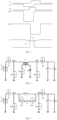
- control unit to control each switch transistor and the auxiliary switch transistor Sa is provided.
- the control unit Before the first switch transistor S1 and the third switch transistor S3 are turned on, the control unit turns off the second switch transistor S2 and the fourth switch transistor S4 first, and then turns on the auxiliary switch transistor Sa; and before the second switch transistor S2 and the fourth switch transistor S4 are turned on, the control unit turns off the first switch transistor S1 and the third switch transistor S3 first, and then turns on the auxiliary switch transistor Sa.
- the difference between the implementation in this embodiment and the implementation in the foregoing embodiment mainly lies in that: in the foregoing embodiment, before the first switch transistor S1 and the third switch transistor S3 are turned on, the control unit turns on the auxiliary switch transistor Sa first, and then turns off the second switch transistor S2 and the fourth switch transistor S4.
- the auxiliary switch transistor Sa is turned on before the second switch transistor S2 and the fourth switch transistor S4 are turned off, the voltage on the equivalent inductor continues to be equal to Vo for a period of time and starts to decrease after the second switch transistor S2 and the fourth switch transistor S4 are turned off; therefore, the increase speed of the current ILa on La is fast, which allows for implementation of zero-voltage turn-on of the first switch transistor S1 and the third switch transistor S3 at the same time, but the large current ILa on La increases the loss of the entire soft switch circuit in a turn-on state, as well as the turn-off loss of each switch transistor.
- the control unit turns off the second switch transistor S2 and the fourth switch transistor S4 first, and then turns on the auxiliary switch transistor Sa.
- the voltage on the equivalent inductor starts to decrease from Vo.
- the increase speed of the current ILa on La is slow, and the current ILa on La is smaller, which can effectively reduce the loss of the entire soft switch circuit in a turn-on state as well as the turn-off loss of each switch transistor.
- the current of the equivalent inductor may decrease Vsw2 synchronously while increasing Vsw1.
- Fig. 3 shows an example in which the first switch transistor S1 is turned on first, so as to ensure implementation of zero-voltage turn-on of both switch transistors, and reduce the switching loss of the entire soft switch circuit.
- the second switch transistor S2 and the fourth switch transistor S4 may be turned on sequentially at a second preset time interval, and the first preset time interval and the second preset time interval may be equal or may be unequal.
- the control unit controls the first switch transistor S1 and the third switch transistor S3 to be turned on at the same time, that is, the first preset time interval is 0, and the control unit controls the second switch transistor S2 and the fourth switch transistor S4 to be turned on at the same time, that is, the second preset time interval is 0.
- the control unit may be directly configured to control the first switch transistor and the third switch transistor to be turned on at the same time, thereby simplifying the control policy.
- control unit may also turn off the auxiliary switch transistor Sa after the first switch transistor S1 and the third switch transistor S3 are turned on; and turn off the auxiliary switch transistor Sa after the second switch transistor S2 and the fourth switch transistor S4 are turned on.
- the auxiliary switch transistor may be turned off after the first switch transistor and the third switch transistor are turned on, so as to decrease the current of the auxiliary branch circuit when the auxiliary switch transistor is turned off as far as possible, thereby reducing the turn-off loss generated by turning off the auxiliary switch transistor, and further reducing the switching loss of the entire soft switch circuit.
- control unit may specifically turn off the auxiliary switch transistor Sa after the first switch transistor S1 and the third switch transistor S3 are turned on and when the current on the auxiliary branch circuit is 0; and turn off the auxiliary switch transistor Sa after the second switch transistor S2 and the fourth switch transistor S4 are turned on and when the current on the auxiliary branch circuit is 0.
- the control switch when the current on the auxiliary branch circuit is equal to 0, the control switch specifically turns off the auxiliary switch transistor, so as to implement zero-current turn-off of the auxiliary switch transistor, thereby further reducing the turn-off loss generated by turning off the auxiliary switch transistor, and further reducing the switching loss of the entire soft switch circuit.
- the soft switch circuit further includes an auxiliary diode Da, the auxiliary diode Da is provided on the auxiliary branch circuit, and a conducting direction of the auxiliary diode Da on the auxiliary branch circuit is from the second end of the main inductor L1 to the first end of the main inductor L1.
- the specific position of the auxiliary diode Da on the auxiliary branch circuit is not limited herein.
- Fig. 1 shows an example in which the auxiliary diode Da is provided between the auxiliary inductor La and the second end of the main inductor L1.
- the current of the equivalent inductor flowing from the second end to the first end of the main inductor may decrease to 0, and the current reversely flows from the first end to the second end of the main inductor.
- the current on the auxiliary switch transistor is 0, and turning off the auxiliary switch transistor in this period of time can implement zero-current turn-off of the auxiliary switch transistor, so as to further reduce the switching loss of the entire soft switch circuit.
- the auxiliary inductor La is magnetically coupled in parallel to the main inductor L1.
- a coil of the auxiliary inductor La is provided on a magnetic core of the main inductor L1, and the auxiliary inductor La exchanges energy with the main inductor L1 by using a magnetic field.
- the auxiliary inductor is magnetically coupled in parallel to the main inductor.
- a coil of the auxiliary inductor is directly provided on a magnetic core of the main inductor to form a coupled inductor together with the main inductor, without an additional magnetic core, thereby reducing the volume of the entire soft switch circuit to a certain extent; energy is directly transferred between the auxiliary inductor and the main inductor by using a magnetic field, thereby realizing electrical isolation between the main inductor and the auxiliary inductor, without adding an isolation apparatus.
- two ends of an auxiliary branch circuit may be connected to other potentials, for example, both are connected to the same reference ground as that of a control unit, and it is unnecessary to perform floating driving on an auxiliary switch transistor, thereby reducing driving requirements.
- the auxiliary switch transistor Sa includes a first auxiliary MOS transistor Sa1 and a second auxiliary MOS transistor Sa2 connected in series, wherein a conducting direction of the body diode of the first auxiliary MOS transistor Sa1 on the auxiliary branch circuit is from the first end of the main inductor L1 to the second end of the main inductor L1, and a conducting direction of the body diode of the second auxiliary MOS transistor Sa2 on the auxiliary branch circuit is from the second end of the main inductor L1 to the first end of the main inductor L1.
- the control unit turns on the first auxiliary MOS transistor Sa1, and turns off the second auxiliary MOS transistor Sa2.
- the direction of the body diode of the second auxiliary MOS transistor Sa2 is obviously the same as the direction of the auxiliary diode Da in the embodiment corresponding to Fig. 1 . Therefore, zero-current turn-off of the auxiliary switch transistor can also be implemented, so as to further reduce the switching loss of the entire soft switch circuit.
- the control unit Before the second switch transistor S2 and the fourth switch transistor S4 are turned on, the control unit turns on the second auxiliary MOS transistor Sa2, and turns off the first auxiliary MOS transistor Sa1.
- the body diode of the first auxiliary MOS transistor Sa1 can also implement zero-current turn-off of the auxiliary switch transistor, so as to further reduce the switching loss of the entire soft switch circuit.
- the control unit turns on the second auxiliary MOS transistor Sa2, and turns off the first auxiliary MOS transistor Sa1; and before the second switch transistor S2 and the fourth switch transistor S4 are turned on, the control unit turns on the first auxiliary MOS transistor Sa1, and turns off the second auxiliary MOS transistor Sa2.
- a coil of the auxiliary inductor La is provided on a magnetic core of the main inductor L1.
- one end of the first auxiliary MOS transistor Sa1 and one end of the second auxiliary MOS transistor Sa2 on two sides of the auxiliary inductor La can be connected to the same reference ground as that of a control unit, and it is unnecessary to perform floating driving on the first auxiliary MOS transistor Sa1 and the second auxiliary MOS transistor Sa2, thereby reducing driving requirements.
- each MOS transistor when electric energy is transmitted bi-directionally between a power supply and a capacitor, each MOS transistor is enabled to implement zero-voltage turn-on, the implementation principle is the same as that in the foregoing embodiment, and zero-current turn-off of an auxiliary switch transistor can also be implemented, so as to further reduce the switching loss of the entire soft switch circuit.
- An embodiment of the present disclosure relates to a circuit board assembly including the soft switch circuit of the foregoing embodiment.
- An embodiment of the present disclosure relates to a switch power supply including the circuit board assembly of the foregoing embodiment.
Landscapes
- Engineering & Computer Science (AREA)
- Power Engineering (AREA)
- Dc-Dc Converters (AREA)
Applications Claiming Priority (2)
| Application Number | Priority Date | Filing Date | Title |
|---|---|---|---|
| CN202110898020.5A CN115912868A (zh) | 2021-08-05 | 2021-08-05 | 一种软开关电路、电路板组件及开关电源 |
| PCT/CN2021/135795 WO2023010733A1 (zh) | 2021-08-05 | 2021-12-06 | 一种软开关电路、电路板组件及开关电源 |
Publications (2)
| Publication Number | Publication Date |
|---|---|
| EP4383544A1 true EP4383544A1 (de) | 2024-06-12 |
| EP4383544A4 EP4383544A4 (de) | 2024-11-13 |
Family
ID=85155057
Family Applications (1)
| Application Number | Title | Priority Date | Filing Date |
|---|---|---|---|
| EP21952596.1A Pending EP4383544A4 (de) | 2021-08-05 | 2021-12-06 | Weicher schaltkreis, leiterplattenanordnung und schaltnetzteil |
Country Status (5)
| Country | Link |
|---|---|
| US (1) | US20240313629A1 (de) |
| EP (1) | EP4383544A4 (de) |
| JP (1) | JP2024528276A (de) |
| CN (1) | CN115912868A (de) |
| WO (1) | WO2023010733A1 (de) |
Families Citing this family (1)
| Publication number | Priority date | Publication date | Assignee | Title |
|---|---|---|---|---|
| US20250149982A1 (en) * | 2023-11-03 | 2025-05-08 | Texas Instruments Incorporated | Power converter with auxiliary inductor |
Family Cites Families (11)
| Publication number | Priority date | Publication date | Assignee | Title |
|---|---|---|---|---|
| JP4017490B2 (ja) * | 2002-10-02 | 2007-12-05 | 株式会社デンソー | Dc/dcコンバータ |
| JP2005176540A (ja) * | 2003-12-12 | 2005-06-30 | Toyota Motor Corp | 電圧変換装置 |
| JP4891789B2 (ja) * | 2007-01-18 | 2012-03-07 | 株式会社リコー | 印刷システム、電子装置、及びプログラム |
| JP2008306884A (ja) * | 2007-06-11 | 2008-12-18 | Nissan Motor Co Ltd | 電圧変換装置 |
| JP5223299B2 (ja) * | 2007-10-31 | 2013-06-26 | 日産自動車株式会社 | コンバータ回路およびコンバータ制御方法 |
| US20170005563A1 (en) * | 2014-01-07 | 2017-01-05 | Arizona Board Of Regents On Behalf Of Arizona State University | Zero-Voltage Transition in Power Converters with an Auxiliary Circuit |
| JP6748489B2 (ja) * | 2016-06-22 | 2020-09-02 | 株式会社デンソー | 電力変換装置 |
| CN106208698B (zh) * | 2016-08-09 | 2018-11-09 | 中南大学 | 设有软开关的四开关Buck-Boost变换器电路及其控制方法 |
| CN114915173B (zh) * | 2021-02-08 | 2026-04-21 | 台达电子工业股份有限公司 | 柔切式电源转换器 |
| CN115224909A (zh) * | 2021-03-31 | 2022-10-21 | Tdk株式会社 | 电力转换装置 |
| US20230020072A1 (en) * | 2021-07-19 | 2023-01-19 | Analog Devices, Inc. | Zero-voltage switching for buck-boost converter |
-
2021
- 2021-08-05 CN CN202110898020.5A patent/CN115912868A/zh active Pending
- 2021-12-06 EP EP21952596.1A patent/EP4383544A4/de active Pending
- 2021-12-06 WO PCT/CN2021/135795 patent/WO2023010733A1/zh not_active Ceased
- 2021-12-06 JP JP2024507008A patent/JP2024528276A/ja active Pending
- 2021-12-06 US US18/681,213 patent/US20240313629A1/en active Pending
Also Published As
| Publication number | Publication date |
|---|---|
| EP4383544A4 (de) | 2024-11-13 |
| JP2024528276A (ja) | 2024-07-26 |
| WO2023010733A1 (zh) | 2023-02-09 |
| CN115912868A (zh) | 2023-04-04 |
| US20240313629A1 (en) | 2024-09-19 |
Similar Documents
| Publication | Publication Date | Title |
|---|---|---|
| CN108683332B (zh) | 一种高增益、宽占空比控制Boost变换器 | |
| US7706156B2 (en) | Resonant converter with synchronous rectification drive circuit | |
| CN101686015B (zh) | 具有主动箝位电路的正-反激变换器 | |
| CN100511942C (zh) | 正反激双向dc-dc变换器的控制方法 | |
| Song et al. | Dual-bridge DC-DC converter: A new topology characterized with no deadtime operation | |
| CN108199579B (zh) | 一种带耦合电感的高变比软开关dc-dc降压变换器 | |
| WO2019001216A1 (zh) | 一种有源钳位正激式开关电源电路 | |
| CN110994982B (zh) | 一种软开关方式的buck变换器及其控制方法 | |
| CN114915173A (zh) | 柔切式电源转换器 | |
| US10348205B1 (en) | Coupled-inductor cascaded buck converter with fast transient response | |
| CN104734496B (zh) | 一种sepic馈电升降压变换器 | |
| CN210444179U (zh) | 一种buck电流馈电推挽拓扑串联谐振电路 | |
| EP4383544A1 (de) | Weicher schaltkreis, leiterplattenanordnung und schaltnetzteil | |
| CN108322053B (zh) | 一种降压式变换电路 | |
| CN106787737B (zh) | 一种双向直流变换器 | |
| CN115021571A (zh) | 一种隔离驱动控制电路及驱动控制方法 | |
| CN107222109A (zh) | 一种含有源缓冲器的双向隔离式dc‑dc变换器 | |
| CN216751537U (zh) | 一种应用于降压变换器的直通电路 | |
| CN112491280B (zh) | 一种正反激变换器的输出倍压电路 | |
| KR102413600B1 (ko) | 자기구동 동기 스위치를 이용한 비절연 고전압 출력 dc-dc 컨버터 | |
| CN108111003B (zh) | 一种晶闸管驱动电路及方法 | |
| Hwu et al. | DC-DC converter with large step-down voltage conversion ratio | |
| Gang et al. | A novel soft switching bi-directional DC/DC converter | |
| CN112187045A (zh) | 一种无负向电流的buck变换器自举驱动电路 | |
| CN215772920U (zh) | 一种高增益反激式变换器 |
Legal Events
| Date | Code | Title | Description |
|---|---|---|---|
| STAA | Information on the status of an ep patent application or granted ep patent |
Free format text: STATUS: THE INTERNATIONAL PUBLICATION HAS BEEN MADE |
|
| PUAI | Public reference made under article 153(3) epc to a published international application that has entered the european phase |
Free format text: ORIGINAL CODE: 0009012 |
|
| STAA | Information on the status of an ep patent application or granted ep patent |
Free format text: STATUS: REQUEST FOR EXAMINATION WAS MADE |
|
| 17P | Request for examination filed |
Effective date: 20240305 |
|
| AK | Designated contracting states |
Kind code of ref document: A1 Designated state(s): AL AT BE BG CH CY CZ DE DK EE ES FI FR GB GR HR HU IE IS IT LI LT LU LV MC MK MT NL NO PL PT RO RS SE SI SK SM TR |
|
| A4 | Supplementary search report drawn up and despatched |
Effective date: 20241015 |
|
| DAV | Request for validation of the european patent (deleted) | ||
| DAX | Request for extension of the european patent (deleted) | ||
| RIC1 | Information provided on ipc code assigned before grant |
Ipc: H03K 17/16 20060101ALI20241009BHEP Ipc: H03K 17/13 20060101ALI20241009BHEP Ipc: H02M 1/00 20060101ALI20241009BHEP Ipc: H02M 3/158 20060101AFI20241009BHEP |