EP4383961A1 - Verfahren zur selektiven strukturierung einer membran - Google Patents
Verfahren zur selektiven strukturierung einer membran Download PDFInfo
- Publication number
- EP4383961A1 EP4383961A1 EP22211939.8A EP22211939A EP4383961A1 EP 4383961 A1 EP4383961 A1 EP 4383961A1 EP 22211939 A EP22211939 A EP 22211939A EP 4383961 A1 EP4383961 A1 EP 4383961A1
- Authority
- EP
- European Patent Office
- Prior art keywords
- ink
- membrane
- pores
- free
- filled
- Prior art date
- Legal status (The legal status is an assumption and is not a legal conclusion. Google has not performed a legal analysis and makes no representation as to the accuracy of the status listed.)
- Withdrawn
Links
Images

Classifications
-
- H—ELECTRICITY
- H05—ELECTRIC TECHNIQUES NOT OTHERWISE PROVIDED FOR
- H05K—PRINTED CIRCUITS; CASINGS OR CONSTRUCTIONAL DETAILS OF ELECTRIC APPARATUS; MANUFACTURE OF ASSEMBLAGES OF ELECTRICAL COMPONENTS
- H05K3/00—Apparatus or processes for manufacturing printed circuits
- H05K3/40—Forming printed elements for providing electric connections to or between printed circuits
- H05K3/42—Plated through-holes or plated via connections
- H05K3/423—Plated through-holes or plated via connections characterised by electroplating method
-
- H—ELECTRICITY
- H05—ELECTRIC TECHNIQUES NOT OTHERWISE PROVIDED FOR
- H05K—PRINTED CIRCUITS; CASINGS OR CONSTRUCTIONAL DETAILS OF ELECTRIC APPARATUS; MANUFACTURE OF ASSEMBLAGES OF ELECTRICAL COMPONENTS
- H05K1/00—Printed circuits
- H05K1/02—Details
- H05K1/09—Use of materials for the conductive, e.g. metallic pattern
-
- H—ELECTRICITY
- H05—ELECTRIC TECHNIQUES NOT OTHERWISE PROVIDED FOR
- H05K—PRINTED CIRCUITS; CASINGS OR CONSTRUCTIONAL DETAILS OF ELECTRIC APPARATUS; MANUFACTURE OF ASSEMBLAGES OF ELECTRICAL COMPONENTS
- H05K3/00—Apparatus or processes for manufacturing printed circuits
- H05K3/0073—Masks not provided for in groups H05K3/02 - H05K3/46, e.g. for photomechanical production of patterned surfaces
- H05K3/0079—Masks not provided for in groups H05K3/02 - H05K3/46, e.g. for photomechanical production of patterned surfaces characterised by the method of application or removal of the mask
-
- B—PERFORMING OPERATIONS; TRANSPORTING
- B82—NANOTECHNOLOGY
- B82Y—SPECIFIC USES OR APPLICATIONS OF NANOSTRUCTURES; MEASUREMENT OR ANALYSIS OF NANOSTRUCTURES; MANUFACTURE OR TREATMENT OF NANOSTRUCTURES
- B82Y40/00—Manufacture or treatment of nanostructures
-
- H—ELECTRICITY
- H05—ELECTRIC TECHNIQUES NOT OTHERWISE PROVIDED FOR
- H05K—PRINTED CIRCUITS; CASINGS OR CONSTRUCTIONAL DETAILS OF ELECTRIC APPARATUS; MANUFACTURE OF ASSEMBLAGES OF ELECTRICAL COMPONENTS
- H05K2201/00—Indexing scheme relating to printed circuits covered by H05K1/00
- H05K2201/02—Fillers; Particles; Fibers; Reinforcement materials
- H05K2201/0203—Fillers and particles
- H05K2201/0242—Shape of an individual particle
- H05K2201/026—Nanotubes or nanowires
-
- H—ELECTRICITY
- H05—ELECTRIC TECHNIQUES NOT OTHERWISE PROVIDED FOR
- H05K—PRINTED CIRCUITS; CASINGS OR CONSTRUCTIONAL DETAILS OF ELECTRIC APPARATUS; MANUFACTURE OF ASSEMBLAGES OF ELECTRICAL COMPONENTS
- H05K2203/00—Indexing scheme relating to apparatus or processes for manufacturing printed circuits covered by H05K3/00
- H05K2203/01—Tools for processing; Objects used during processing
- H05K2203/0104—Tools for processing; Objects used during processing for patterning or coating
- H05K2203/013—Inkjet printing, e.g. for printing insulating material or resist
Definitions
- a selectively structured membrane having ink-filled pores and ink-free pores is received.
- the ink that has entered the pores serves for clogging these pores, wherein the other pores remain open. Since the ink is applied onto the first surface of the membrane in a structured manner (i.e., representing a space-resolved pattern covering only a part of the membrane, wherein other parts of the membrane remain free of ink), no undesired accidental clogging of pores that should remain open will occur. Rather, the ink will only enter into those pores that are in the membrane region that has been previously covered with the ink.
- the ink-filled pores may also be denoted as closed pores, wherein the ink-free pores may be denoted as open pores.
- the selectively structured membrane comprises open pores and closed pores distributed over the membrane in a defined manner corresponding to the applied structuring by the deposited ink.
- the membrane is passivated at the printed sites (i.e. in all areas in which the ink has been applied to the surface of the membrane and has been entered into the pores of the membrane).
- the inkjet application process has a very high spatial resolution and thus allows to selectively close some of the pores of the membrane in a finely structured manner. Consequently, the properties of the membrane are selectively changed and can afterwards be used in a spatially selective manner.
- Such selectively structured membrane allows a selective permeability for specific compounds.
- the membrane can be used for filtering specific substances or for transporting ions.
- a gas-permeable membrane can be used for manufacturing a sensor.
- the residual ink is, in an embodiment, removed in a dry state of the residual ink. Then, such risk of clogging pores in the ink-free portions of the membrane is significantly reduced or even totally avoided.
- the ink enters into the pores simply by gravity or by the capillary forces of the pores, as outlined above.
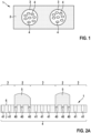
- ink-covered portions 2 as well as ink-free portions 3 of the membrane 1 are formed.
- the ink 5 applied onto the first surface 6 of the membrane 1 enters the pores 4 being present in the ink-covered portions 2 and advances towards a second surface 7 of the membrane 1 being opposite the first surface 6. It should be noted that the ink 5 is applied onto the first surface 6 in a spatially resolved manner by printing very fine structures onto the membrane 1.
Landscapes
- Engineering & Computer Science (AREA)
- Microelectronics & Electronic Packaging (AREA)
- Manufacturing & Machinery (AREA)
- Separation Using Semi-Permeable Membranes (AREA)
Priority Applications (1)
| Application Number | Priority Date | Filing Date | Title |
|---|---|---|---|
| EP22211939.8A EP4383961A1 (de) | 2022-12-07 | 2022-12-07 | Verfahren zur selektiven strukturierung einer membran |
Applications Claiming Priority (1)
| Application Number | Priority Date | Filing Date | Title |
|---|---|---|---|
| EP22211939.8A EP4383961A1 (de) | 2022-12-07 | 2022-12-07 | Verfahren zur selektiven strukturierung einer membran |
Publications (1)
| Publication Number | Publication Date |
|---|---|
| EP4383961A1 true EP4383961A1 (de) | 2024-06-12 |
Family
ID=84439978
Family Applications (1)
| Application Number | Title | Priority Date | Filing Date |
|---|---|---|---|
| EP22211939.8A Withdrawn EP4383961A1 (de) | 2022-12-07 | 2022-12-07 | Verfahren zur selektiven strukturierung einer membran |
Country Status (1)
| Country | Link |
|---|---|
| EP (1) | EP4383961A1 (de) |
Citations (3)
| Publication number | Priority date | Publication date | Assignee | Title |
|---|---|---|---|---|
| US20130014799A1 (en) * | 2005-08-22 | 2013-01-17 | Ruxandra Vidu | Nanostructure and photovoltaic cell implementing same |
| US20190016909A1 (en) * | 2016-01-11 | 2019-01-17 | University Of Notre Dame Du Lac | Template synthesis of polymeric nanomaterials by ink-jet printing |
| CN111765908A (zh) * | 2019-04-02 | 2020-10-13 | 天津大学 | 基于模板法制备银纳米线嵌入pdms柔性电容传感器的方法 |
-
2022
- 2022-12-07 EP EP22211939.8A patent/EP4383961A1/de not_active Withdrawn
Patent Citations (3)
| Publication number | Priority date | Publication date | Assignee | Title |
|---|---|---|---|---|
| US20130014799A1 (en) * | 2005-08-22 | 2013-01-17 | Ruxandra Vidu | Nanostructure and photovoltaic cell implementing same |
| US20190016909A1 (en) * | 2016-01-11 | 2019-01-17 | University Of Notre Dame Du Lac | Template synthesis of polymeric nanomaterials by ink-jet printing |
| CN111765908A (zh) * | 2019-04-02 | 2020-10-13 | 天津大学 | 基于模板法制备银纳米线嵌入pdms柔性电容传感器的方法 |
Non-Patent Citations (1)
| Title |
|---|
| PENG GAO ET AL: "Template Synthesis of Nanostructured Polymeric Membranes by Inkjet Printing", APPLIED MATERIALS & INTERFACES, vol. 8, no. 5, 10 February 2016 (2016-02-10), US, pages 3386 - 3395, XP055399464, ISSN: 1944-8244, DOI: 10.1021/acsami.5b11360 * |
Similar Documents
| Publication | Publication Date | Title |
|---|---|---|
| EP1341655B1 (de) | Verfahren zur herstellung eines mikro- oder nanostrukturierten produktes | |
| US8372297B2 (en) | Method for fabricating membrane having hydrophilicity and hydrophobicity | |
| KR102375841B1 (ko) | 가요성 기판상에 전자 장치를 형성하는 방법 | |
| JP5651707B2 (ja) | 多孔質基材に液流案内構造を製造する方法 | |
| WO2005102910A1 (de) | Verkapseltes elektrisches bauelement und verfahren zur herstellung | |
| WO2001037050A1 (de) | Verwendung von polyimid für haftschichten, lithographisches verfahren zur herstellung von mikrobauteilen sowie verfahren zur herstellung von verbundmaterial | |
| US5633664A (en) | Method of influencing the contact angle of the nozzle surface of inkjet printheads | |
| EP4383961A1 (de) | Verfahren zur selektiven strukturierung einer membran | |
| EP1675725A1 (de) | Elastomerer stempel, mustererzeugungsverfahren unter verwendung solch eines stempels und verfahren zur herstellung solch eines stempels | |
| EP1198344A1 (de) | Verfahren zum herstellen von mikrobauteilen | |
| US9781829B2 (en) | Surface pretreatment and drop spreading control on multi component surfaces | |
| DE10308820A1 (de) | Sensor, Meßzelle zur Verwendung in einem Sensor und Verfahren zur Herstellung einer Meßzelle | |
| DE102015223399B4 (de) | Verfahren zum Verpacken mindestens eines Halbleiterbauteils und Halbleitervorrichtung | |
| DE102006052693A1 (de) | Verfahren zur Fertigung eines Halbleitersensors | |
| KR101716851B1 (ko) | 용액재료를 이용한 미세패턴 제조방법 | |
| WO2006005487A1 (de) | Mikrostrukturierte vorrichtung und verfahren zu ihrer herstellung | |
| JP5863923B1 (ja) | スクリーン印刷版およびその製造方法 | |
| Hammerschmidt et al. | Characterization of fully inkjet-printed microsieves and of patterns for the mechanical reinforcement of fragile membranes | |
| JP2000033685A (ja) | ロータリースクリーン印刷用シリンダー及びその製造方法 | |
| CN101924032B (zh) | 掩蔽方法 | |
| DE102009006064B4 (de) | Verfahren zur Herstellung eines mikrostrukturierten Films | |
| DE102008045540B4 (de) | Verfahren zur Herstellung eines mikrostrukturierten Films | |
| EP4049845B1 (de) | Flüssigkeitsausstosskartusche und verfahren zur herstellung einer sintermetallpatrone | |
| KR101460072B1 (ko) | 고해상도 마이크로 패턴의 제조방법 | |
| EP2200930B1 (de) | Verfahren zum aufdrucken einer nano- und/oder mikrostruktur |
Legal Events
| Date | Code | Title | Description |
|---|---|---|---|
| PUAI | Public reference made under article 153(3) epc to a published international application that has entered the european phase |
Free format text: ORIGINAL CODE: 0009012 |
|
| STAA | Information on the status of an ep patent application or granted ep patent |
Free format text: STATUS: THE APPLICATION HAS BEEN PUBLISHED |
|
| AK | Designated contracting states |
Kind code of ref document: A1 Designated state(s): AL AT BE BG CH CY CZ DE DK EE ES FI FR GB GR HR HU IE IS IT LI LT LU LV MC ME MK MT NL NO PL PT RO RS SE SI SK SM TR |
|
| STAA | Information on the status of an ep patent application or granted ep patent |
Free format text: STATUS: THE APPLICATION IS DEEMED TO BE WITHDRAWN |
|
| 18D | Application deemed to be withdrawn |
Effective date: 20241213 |