EP4386794A2 - Composant électronique multicouche - Google Patents
Composant électronique multicouche Download PDFInfo
- Publication number
- EP4386794A2 EP4386794A2 EP23205242.3A EP23205242A EP4386794A2 EP 4386794 A2 EP4386794 A2 EP 4386794A2 EP 23205242 A EP23205242 A EP 23205242A EP 4386794 A2 EP4386794 A2 EP 4386794A2
- Authority
- EP
- European Patent Office
- Prior art keywords
- electrode layer
- layer
- disposed
- electrode
- electronic component
- Prior art date
- Legal status (The legal status is an assumption and is not a legal conclusion. Google has not performed a legal analysis and makes no representation as to the accuracy of the status listed.)
- Pending
Links
Images




Classifications
-
- H—ELECTRICITY
- H01—ELECTRIC ELEMENTS
- H01G—CAPACITORS; CAPACITORS, RECTIFIERS, DETECTORS, SWITCHING DEVICES, LIGHT-SENSITIVE OR TEMPERATURE-SENSITIVE DEVICES OF THE ELECTROLYTIC TYPE
- H01G4/00—Fixed capacitors; Processes of their manufacture
- H01G4/002—Details
- H01G4/005—Electrodes
- H01G4/008—Selection of materials
-
- H—ELECTRICITY
- H01—ELECTRIC ELEMENTS
- H01G—CAPACITORS; CAPACITORS, RECTIFIERS, DETECTORS, SWITCHING DEVICES, LIGHT-SENSITIVE OR TEMPERATURE-SENSITIVE DEVICES OF THE ELECTROLYTIC TYPE
- H01G4/00—Fixed capacitors; Processes of their manufacture
- H01G4/002—Details
- H01G4/005—Electrodes
-
- H—ELECTRICITY
- H01—ELECTRIC ELEMENTS
- H01G—CAPACITORS; CAPACITORS, RECTIFIERS, DETECTORS, SWITCHING DEVICES, LIGHT-SENSITIVE OR TEMPERATURE-SENSITIVE DEVICES OF THE ELECTROLYTIC TYPE
- H01G4/00—Fixed capacitors; Processes of their manufacture
- H01G4/002—Details
- H01G4/005—Electrodes
- H01G4/012—Form of non-self-supporting electrodes
-
- H—ELECTRICITY
- H01—ELECTRIC ELEMENTS
- H01G—CAPACITORS; CAPACITORS, RECTIFIERS, DETECTORS, SWITCHING DEVICES, LIGHT-SENSITIVE OR TEMPERATURE-SENSITIVE DEVICES OF THE ELECTROLYTIC TYPE
- H01G4/00—Fixed capacitors; Processes of their manufacture
- H01G4/002—Details
- H01G4/018—Dielectrics
- H01G4/06—Solid dielectrics
- H01G4/08—Inorganic dielectrics
- H01G4/12—Ceramic dielectrics
-
- H—ELECTRICITY
- H01—ELECTRIC ELEMENTS
- H01G—CAPACITORS; CAPACITORS, RECTIFIERS, DETECTORS, SWITCHING DEVICES, LIGHT-SENSITIVE OR TEMPERATURE-SENSITIVE DEVICES OF THE ELECTROLYTIC TYPE
- H01G4/00—Fixed capacitors; Processes of their manufacture
- H01G4/002—Details
- H01G4/228—Terminals
- H01G4/232—Terminals electrically connecting two or more layers of a stacked or rolled capacitor
- H01G4/2325—Terminals electrically connecting two or more layers of a stacked or rolled capacitor characterised by the material of the terminals
-
- H—ELECTRICITY
- H01—ELECTRIC ELEMENTS
- H01G—CAPACITORS; CAPACITORS, RECTIFIERS, DETECTORS, SWITCHING DEVICES, LIGHT-SENSITIVE OR TEMPERATURE-SENSITIVE DEVICES OF THE ELECTROLYTIC TYPE
- H01G4/00—Fixed capacitors; Processes of their manufacture
- H01G4/30—Stacked capacitors
-
- H—ELECTRICITY
- H01—ELECTRIC ELEMENTS
- H01G—CAPACITORS; CAPACITORS, RECTIFIERS, DETECTORS, SWITCHING DEVICES, LIGHT-SENSITIVE OR TEMPERATURE-SENSITIVE DEVICES OF THE ELECTROLYTIC TYPE
- H01G4/00—Fixed capacitors; Processes of their manufacture
- H01G4/002—Details
- H01G4/018—Dielectrics
- H01G4/06—Solid dielectrics
- H01G4/08—Inorganic dielectrics
- H01G4/12—Ceramic dielectrics
- H01G4/1209—Ceramic dielectrics characterised by the ceramic dielectric material
- H01G4/1218—Ceramic dielectrics characterised by the ceramic dielectric material based on titanium oxides or titanates
- H01G4/1227—Ceramic dielectrics characterised by the ceramic dielectric material based on titanium oxides or titanates based on alkaline earth titanates
-
- H—ELECTRICITY
- H01—ELECTRIC ELEMENTS
- H01G—CAPACITORS; CAPACITORS, RECTIFIERS, DETECTORS, SWITCHING DEVICES, LIGHT-SENSITIVE OR TEMPERATURE-SENSITIVE DEVICES OF THE ELECTROLYTIC TYPE
- H01G4/00—Fixed capacitors; Processes of their manufacture
- H01G4/002—Details
- H01G4/228—Terminals
- H01G4/232—Terminals electrically connecting two or more layers of a stacked or rolled capacitor
Definitions
- the present disclosure relates to a multilayer electronic component.
- a multilayer ceramic capacitor (MLCC), a multilayer electronic component may be a chip-type condenser mounted on the printed circuit boards of any of various types of electronic products, such as an imaging device, including a liquid crystal display (LCD) or a plasma display panel (PDP), a computer, a smartphone, or a mobile phone, serving to charge or discharge electricity therein or therefrom.
- an imaging device including a liquid crystal display (LCD) or a plasma display panel (PDP), a computer, a smartphone, or a mobile phone, serving to charge or discharge electricity therein or therefrom.
- LCD liquid crystal display
- PDP plasma display panel
- Such a multilayer ceramic capacitor may have a reduced size, may implement high capacitance, and may be easily mounted on a circuit board, and may thus be used as a component of various electronic devices.
- a multilayer ceramic capacitor has been increasing demand for a multilayer ceramic capacitor to have a reduced size and higher capacitance as each of various electronic devices such as a computer and a mobile device have a reduced size and higher output.
- a layer including a metal oxide may be formed between layers of the external electrodes, and the oxide layer may cause deterioration of interlayer adhesion of the external electrodes.
- One of several objects of the present disclosure is to suppress deterioration of insulation resistance (IR) of a multilayer electronic component in a high-temperature and high-humidity environment.
- IR insulation resistance
- One of the various objects of the present disclosure is to suppress deterioration of moisture resistance reliability of a multilayer electronic component due to deterioration of interlayer adhesion due to formation of oxides between electrode layers in a multilayer structure of external electrodes.
- the object of the present invention is not limited to the above, and will be more easily understood in the process of describing specific embodiments of the present disclosure.
- a multilayer electronic component includes: a body including a dielectric layer and an internal electrode; and an external electrode disposed on the body.
- the external electrode includes a first electrode layer connected to the internal electrodes and including Cu, a second electrode layer partially disposed on the first electrode layer and including Ni, an intermediate layer disposed on the second electrode layer and in a region of the first electrode layer, in which a second electrode layer is not disposed, and including a metal oxide, and a first plating layer disposed on the intermediate layer and including Ni.
- a multilayer electronic component includes: a body including a dielectric layer and an internal electrode; an external electrode disposed on the body.
- the external electrode includes a first electrode layer connected to the internal electrodes and including Cu, a second electrode layer disposed on the first electrode layer and including Ni, an intermediate layer disposed on the second electrode layer and including a metal oxide, and a first plating layer disposed on the intermediate layer and including Ni.
- the second electrode layer includes a plurality of openings penetrating through the second electrode layer.
- the intermediate layer is disposed on the second electrode layer and the plurality of openings.
- a multilayer electronic component includes: a body including a dielectric layer and an internal electrode; and an external electrode disposed on the body to connect to the internal electrode.
- the external electrode includes a first electrode layer connected to the internal electrode, a second electrode layer disposed on the first electrode layer and including an opening penetrating through the second electrode layer, a first plating layer covering the second electrode layer and disposed in the opening to cover the first electrode layer, and an oxide layer disposed between the second electrode layer and the first plating layer and disposed in the opening to be between the first electrode layer and the first plating layer.
- a first direction may refer to a stacking direction or a thickness (T) direction
- a second direction may refer to a length (L) direction
- a third direction may refer to a width (W) direction.
- FIG. 1 is a perspective view schematically illustrating a multilayer electronic component according to an embodiment of the present disclosure.
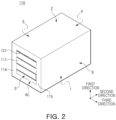
- FIG. 2 is a perspective view schematically illustrating the body of FIG. 1 .
- FIG. 3 is a schematic cross-sectional view taken along line I-I' of FIG. 1 .
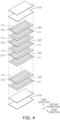
- FIG. 4 is an exploded perspective view illustrating a body of the multilayer electronic component according to an embodiment of the present disclosure.
- FIG. 5 is an enlarged view of region A of FIG. 3 .
- FIG. 6 is an enlarged view of region B of FIG. 5 .
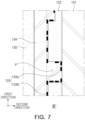
- FIG. 7 is an enlarged view of region B' corresponding to region B of FIG. 5 in an embodiment.
- FIGS. 1 to 7 a multilayer electronic component 100 according to an embodiment in the present disclosure will be described with reference to FIGS. 1 to 7 .
- the multilayer electronic component 100 includes: a body 110 including a dielectric layer 111 and internal electrodes 121 and 122 alternately disposed with the dielectric layer 111 interposed therebetween; and external electrodes 130 and 140 disposed on the body.
- the external electrodes 130 and 140 include a first electrode layer 131 connected to the internal electrodes 121 or 122 and including Cu, a second electrode layer 132 partially disposed on the first electrode layer 131 and including Ni, an intermediate layer 133 disposed in a region of the first electrode layer 131, in which a second electrode layer 132 is not disposed and on the second electrode layer 132 and including a metal oxide, and a first plating layer 134 disposed on the intermediate layer 133 and including Ni.
- the body 110 includes a dielectric layer 111 and internal electrodes 121 and 122 alternately disposed with the dielectric layer 111 interposed therebetween.
- the dielectric layer 111 and the internal electrodes 121 and 122 may be alternately stacked, and the stacking direction may be referred to as a first direction.
- the body 110 is not limited to a particular shape, and may have a hexahedral shape or a shape similar to the hexahedral shape, as illustrated in the drawings.
- the body 110 may not have the shape of a hexahedron having perfectly straight lines because ceramic powder particles included in the body 110 are contracted in a process in which the body is sintered.
- the body 110 may have a substantially hexahedral shape.
- the body 110 may have first and second surfaces 1 and 2 opposing each other in a first direction, third and fourth surfaces 3 and 4 connected to the first and second surfaces 1 and 2 and opposing each other in a second direction, and fifth and sixth surfaces 5 and 6 connected to the first and second surfaces 1 and 2, connected to the third and fourth surfaces 3 and 4, and opposing each other in a third direction.
- a plurality of dielectric layers 111 forming the body 110 may be in a sintered state, and adjacent dielectric layers 111 may be integrated with each other, such that boundaries therebetween may not be readily apparent without a scanning electron microscope (SEM).
- SEM scanning electron microscope
- a raw material for forming the dielectric layer 111 is not particularly limited, as long as sufficient electrostatic capacitance may be obtained therewith.
- the raw material for forming the dielectric layer 111 may be a barium titanate (BaTiO 3 )-based material, a lead composite perovskite-based material, a strontium titanate (SrTiO 3 )-based material, or the like.
- the barium titanate-based material may include BaTiO 3 -based ceramic powder, and the ceramic powder may be, for example, BaTiO 3 , (Ba 1-x Ca x )TiO 3 , Ba(Ti 1-y Ca y )O 3 , (Ba 1-x Ca x )(Ti 1-y Zr y )O 3 or Ba(Ti 1-y Zr y )O 3 , in which calcium (Ca), zirconium (Zr), or the like, are partially dissolved in BaTiO 3 , and the like.
- the ceramic powder may be, for example, BaTiO 3 , (Ba 1-x Ca x )TiO 3 , Ba(Ti 1-y Ca y )O 3 , (Ba 1-x Ca x )(Ti 1-y Zr y )O 3 or Ba(Ti 1-y Zr y )O 3 , in which calcium (Ca), zirconium (Zr), or the like, are partially
- a raw material of the dielectric layer 111 may include various ceramic additives, organic solvents, binders, dispersants, and the like, added to powder particles such as barium titanate (BaTiO 3 ) powder particles, or the like, according to an object of the present disclosure.
- various ceramic additives such as barium titanate (BaTiO 3 ) powder particles, or the like, according to an object of the present disclosure.
- an average thickness "td” of the dielectric layer 111 is not particularly limited. However, in general, when the dielectric layer is thinly formed to have an average thickness of less than 0.6 um, in particular, when the multilayer electronic component is miniaturized as in the case in which the average thickness "td" of the dielectric layer is 0.35 um or less, it may be difficult for reliability to be improved.
- an intermediate layer 133 including a metal oxide is disposed in a region of the first electrode layer 131, in which a second electrode layer 132 is not disposed and on the second electrode layer 132, and a first plating layer 134 including Ni is disposed on the intermediate layer 133, even when an average thickness "td" of the dielectric layer is 0.35 um or less, excellent reliability can be secured.
- the average thickness "td" of the dielectric layer 111 is 0.35 ⁇ m or less, a reliability improvement effect according to the present disclosure may be more remarkable, and miniaturization and high capacitance of the multilayer electronic component may be easily achieved.
- the average thickness "td" of the dielectric layer 111 may mean an average thickness of the dielectric layer 111 disposed between the first and second internal electrodes 121 and 122.
- the average thickness of the dielectric layer 111 may be measured by scanning an image of a cross-section of the body 110 in length and thickness directions (L-T directions) with a scanning electron microscope (SEM) with a magnification of 10,000. More specifically, an average value may be measured by measuring a thickness of one dielectric layer at 30 equally spaced points in the length direction from the scanned image. The 30 points having equal intervals may be designated in the capacitance formation portion Ac. In addition, if the average value is measured by extending the average value measurement to 10 dielectric layers, the average thickness of the dielectric layers can be more generalized.
- the body 110 may include a capacitance formation portion Ac disposed in the body 110, and including a first internal electrode 121 and a second internal electrode 122 disposed to oppose each other with the dielectric layer 111 interposed therebetween and having capacitance formed therein, and cover portions 112 and 113 formed above and below the capacitance formation portion Ac.
- the capacitance formation portion Ac is a portion serving to contribute to capacitance formation of a capacitor, and may be formed by repeatedly stacking a plurality of first and second internal electrodes 121 and 122 with a dielectric layer 111 interposed therebetween.
- the upper cover portion 112 and the lower cover portion 113 may be formed by stacking a single dielectric layer or two or more dielectric layers on the upper and lower surfaces of the capacitance formation portion Ac in a thickness direction, respectively, and the upper cover portion 112 and the lower cover portion 113 may serve to basically prevent damage to the internal electrodes due to physical or chemical stress.
- the upper cover portion 112 and the lower cover portion 113 may not include internal electrodes, and may include the same material as that of the dielectric layer 111. That is, the upper cover portion 112 and the lower cover portion 113 may include a ceramic material, for example, a barium titanate (BaTiO 3 )-based ceramic material.
- a ceramic material for example, a barium titanate (BaTiO 3 )-based ceramic material.
- An average thickness "tc" of the cover portions 112 and 113 need not be particularly limited. However, the average thickness "tc" of the cover portions 112 and 113 may be 20 um or less in order to more easily achieve miniaturization and high capacitance of the multilayer electronic component.
- a second electrode layer 132 including Ni partially disposed on the first electrode layer 131 including Cu is disposed, an intermediate layer 133 including a metal oxide is disposed in a region of the first electrode layer 131 in which a second electrode layer 132 is not disposed and on the second electrode layer 132, and a first plating layer 134 including Ni is disposed on the intermediate layer 133, even when the average thickness "tc" of the cover portions 112 and 113 is 20 ⁇ m or less, excellent reliability can be secured.
- the average thickness "tc" of the cover portions 112 and 113 may mean a size thereof in the first direction, and may be a value obtained by averaging sizes of the cover portions 112 and 113 measured in the first direction at five points having equal intervals above or below the capacitance formation portion Ac.
- margin portions 114 and 115 may be disposed on one surface and the other surface of the capacitance formation portion Ac in the third direction.
- the margin portions 114 and 115 may include a margin portion 114 disposed on the fifth surface 5 of the body 110 and a margin portion 115 disposed on the sixth surface 6 thereof. That is, the margin portions 114 and 115 may be disposed on both side surfaces of the body in a width direction.
- the margin portions 114 and 115 may mean a region between both ends of the first and second internal electrodes 121 and 122 and an interface of the body 110 in a cross-section of the body 110 taken in a width-thickness (W-T) direction, as illustrated in FIG. 2 .
- the margin portions 114 and 115 may basically serve to prevent damages to the internal electrodes due to physical or chemical stresses.
- the margin portions 114 and 115 may be formed by applying a conductive paste to the ceramic green sheet, except where margin portions are to be formed, to form an internal electrode.
- the margin portions 114 and 115 may also be formed by stacking a single dielectric layer or two or more dielectric layers on both side surfaces of the capacitance formation portion Ac in the width direction.
- a width of the margin portions 114 and 115 is not particularly limited. However, in order to more easily implement miniaturization and high capacitance of the multilayer electronic component, an average width of the margin portions 114 and 115 may be 15 um or less.
- the average width of the margin portions 114 and 115 may mean an average size of the margin portions 114 and 115 in a third direction, and may be a value obtained by averaging sizes of the margin portions 114 and 115 measured at five points at equal intervals in the third direction in terms of the capacitance formation portion Ac.
- the internal electrodes 121 and 122 are alternately disposed with the dielectric layer 111.
- the internal electrodes 121 and 122 may include first and second internal electrodes 121 and 122.
- the first and second internal electrodes 121 and 122 may be alternately disposed to oppose each other with the dielectric layer constituting the body 110 interposed therebetween, and may be exposed to (or be in contact with or extend from) the third and fourth surfaces 3 and 4 of the body 110, respectively.
- the first internal electrode 121 may be spaced apart from the fourth surface 4 and exposed through (or be in contact with or extend from) the third surface 3, and the second internal electrode 122 may be spaced apart from the third surface 3 and exposed through (or be in contact with or extend from) the fourth surface 4.
- first and second internal electrodes 121 and 122 may be electrically isolated from each other by the dielectric layer 111 disposed in a middle.
- the body 110 may be formed by alternately stacking a ceramic green sheet on which the first internal electrode 121 is printed and a ceramic green sheet on which the second internal electrode 122 is printed, followed by sintering.
- a material for forming the internal electrodes 121 and 122 are not particularly limited, and as the material, a material having excellent electrical conductivity may be used.
- the internal electrodes 121 and 122 may include one or more of nickel (Ni), copper (Cu), palladium (Pd), silver (Ag), gold (Au), platinum (Pt), tin (Sn), tungsten (W), titanium (Ti), and alloys thereof.
- the internal electrodes 121 and 122 may be formed by printing a conductive paste for the internal electrodes including at least one of nickel (Ni), copper (Cu), palladium (Pd), silver (Ag), gold (Au), platinum (Pt), tin (Sn), tungsten (W), titanium (Ti) and alloys thereof on a ceramic green sheet.
- a method for printing the conductive paste for the internal electrodes may be a screen-printing method or a gravure printing method, but the present disclosure is not limited thereto.
- an average thickness "te" of the internal electrodes 121 and 122 is not particularly limited. However, in general, when the internal electrodes are thinly formed to have a thickness of less than 0.6 um, in particular, when the multilayer electronic component is miniaturized as in the case in which the thickness of the internal electrodes is 0.35 um or less, it may be difficult that moisture resistance reliability is improved.
- an intermediate layer 133 including a metal oxide is disposed in a region of the first electrode layer 131, in which a second electrode layer 132 is not disposed and on the second electrode layer 132, and a first plating layer 134 including Ni is disposed on the intermediate layer 133, even when the average thickness of the internal electrodes 121 and 122 is 0.35 um or less, excellent reliability can be secured.
- the average thickness of the internal electrodes 121 and 122 is 0.35 ⁇ m or less, an effect according to the present disclosure may be more remarkable, and miniaturization and high capacitance of the multilayer electronic component may be easily achieved.
- the average thickness "te" of the internal electrodes 121 and 122 may mean an average thickness of the internal electrodes 121 and 122.
- the average thickness of the internal electrodes 121 and 122 may be measured by scanning an image of a cross-section of the body 110 in length and thickness directions (L-T directions) with a scanning electron microscope (SEM) with a magnification of 10,000. More specifically, an average value may be measured by measuring a thickness of one internal electrode at 30 equally spaced points in the length direction from the scanned image. The 30 points having equal intervals may be designated in the capacitance formation portion Ac. In addition, if the average value is measured by extending the average value measurement to 10 internal electrodes, the average thickness of the internal electrodes can be more generalized.
- External electrodes 130 and 140 are disposed on the body 110.
- the external electrodes 130 and 140 may include a first external electrode 130, in contact with the third surface 3 of the body 110 and a second external electrode 140, in contact with the fourth surface 4 of the body 110.
- the external electrodes 130 and 140 will be described based on the first external electrode 130.
- the description of the first external electrode 130 may be equally applied to the second external electrode 140.
- Insulation resistance (IR) of a multilayer electronic component such as a multilayer ceramic capacitor may be deteriorated in a high-temperature and high-humidity environment. In order to improve this, it is necessary to delay or prevent permeation of moisture or deterioration-causing substances such as hydrogen into the body 110 of the multilayer electronic component 100.
- a method for improving moisture resistance reliability of the multilayer electronic component there is a method of removing residual hydrogen through a heat-treatment process after forming all of the plating layers of the external electrodes.
- a layer including a metal oxide may be formed between layers of the external electrode, and the oxide layer may cause deterioration of interlayer adhesion of the external electrodes.
- the external electrode 130 includes a first electrode layer 131 connected to the internal electrode 121 and including Cu.
- the first electrode layer 131 may include Cu, a conductive metal, and may serve to electrically connect the external electrode 130 to the internal electrode 121 by being connected to the internal electrode 121.
- the first electrode layer 131 may further include one or more of conductive metal elements and alloys thereof in addition to Cu.
- the first electrode layer 131 may include one or more of Ni, Pd, Cr and alloys thereof, in addition to Cu.
- a method of forming the first electrode layer 131 is not particularly limited.
- the first electrode layer 131 may be formed by applying a conductive paste including Cu particles and glass to the third and fourth surfaces 3 and 4 of the body 110, drying and sintering the same, but it is not limited thereto, and may be formed by applying Cu particles to the third and fourth surfaces 3 and 4, drying and sintering the same, by electroplating or electroless plating.
- the external electrode 130 includes an intermediate layer 133 disposed on a region of the first electrode layer 131, in which a second electrode layer 132 is not disposed and on the second electrode layer 132 and including a metal oxide.
- the intermediate layer 133 may be formed by oxidizing conductive metal included in the first electrode layer 131 or the second electrode layer 132. In this case, a thickness of the intermediate layer 133 may be less than a thickness of each of the first electrode layer 131, the second electrode layer 132, and the first plating layer 134.
- the external electrode 130 includes a first plating layer 134 disposed on the intermediate layer 133 and including Ni.
- the first plating layer 134 may include Ni, to serve to improve airtightness of the multilayer electronic component. Therefore, it is preferable that the first plating layer 134 is a plating layer not including glass, but is not limited thereto.
- a method for forming the first plating layer 134 is not particularly limited and may be formed using various plating methods such as electroplating, electroless plating, or the like.
- the external electrode 130 includes a second electrode layer 132 partially disposed on the first electrode layer 131 and including Ni.
- the second electrode layer 132 is partially disposed on the first plating layer 131, even when the intermediate layer 133 including the metal oxide generated in a process of forming the first plating layer 134 is formed in a region of the first electrode layer 131, in which a second electrode layer 132 is not disposed and on the second electrode layer 132, so that interlayer adhesion of the external electrode 130 may be secured.
- the meaning that the second electrode layer 132 is "partially disposed" on the first electrode layer 131 may mean that the second electrode layer 132 is disposed so as not to cover at least a portion of the first electrode layer 131, but it is not limited thereto, which may mean that the second electrode layer 132 has a structure of having a plurality of openings penetrating through the second electrode layer 132, and the second electrode layer 132 has a porous structure having a plurality of pores.
- the second electrode layer 132 may be partially disposed on the first electrode layer 131, to improve an area on which the first plating layer 134 is formed.
- the second electrode layer 132 may act as irregularities on the first electrode layer 131. Accordingly, an anchor effect may be applied to the first plating layer 134. That is, as the second electrode layer 132 is partially disposed on the first electrode layer 131, an area on which the plating layer 134 is formed is increased, and an anchor effect may be caused, so that the interlayer adhesion the external electrode 130 may be improved. Accordingly, moisture resistance reliability of the multilayer electronic component 100 may be improved.
- the intermediate layer 133 may include an oxide including metal included in the first electrode layer 131 and an oxide including metal included in the second electrode layer 132.
- the metal oxide included in the intermediate layer 133 may include at least one of an oxide including Cu and an oxide including Ni.
- the metal oxide included in the intermediate layer 133 may be formed by oxidizing the metal included in the first electrode layer 131 and the second electrode layer 132.
- at least one of oxides including Cu included in the first electrode layer 131 and Ni included in the second electrode layer 132 may be included in the intermediate layer 133.
- the oxide including Cu may be at least one of CuO, Cu 2 O, and Cu 3 O 4
- the oxide including Ni may be NiO, but is not limited thereto.
- the intermediate layer 133 may include an oxide including Cu in a region 133a disposed on the first electrode layer 131 on which the second electrode layer 132 is not disposed, and may include an oxide including Ni in a region 133b disposed on the second electrode layer 132.
- the intermediate layer 133 may be divided into a region 133a disposed on the first electrode layer 131 and a region 133b disposed on the second electrode layer 132.
- the second electrode layer 132 may be deformed into a shape partially disposed on the first electrode layer 131.
- a surface of the second electrode layer 132 and a surface of the first electrode layer 131 may be oxidized.
- the first electrode layer 131 includes Cu, when an oxide including Cu is formed on the surface of the first electrode layer 131, there may be a problem in that adhesion with the first plating layer 134 including Ni may decrease.
- the intermediate layer 133 includes an oxide including Ni in a region 133b disposed on the second electrode layer 132, it is possible to suppress deterioration of the adhesion of the first plating layer 134 may be further suppressed as compared to when the intermediate layer 133 is made of only an oxide including Cu. Accordingly, moisture resistance reliability of the multilayer electronic component 100 can be further improved.
- the intermediate layer 133 may be partially disposed on the first electrode layer 131 and the second electrode layer 132. Since the intermediate layer 133 includes a metal oxide, adhesion with the first plating layer 134 basically including Ni may be weak. In an embodiment, a contact area may be improved by partially disposing the intermediate layer 133 on the first electrode layer 131 and the second electrode layer 132, and the first plating layer 134 may be formed in a gap in which the intermediate layer 133 is partially formed, so that an anchor effect can be maximized. Accordingly, the moisture resistance reliability of the multilayer electronic component 100 can be further improved.
- an average thickness "T" of the first electrode layer 131 may be 2 um or more and 20 um or less.
- the average thickness "T" of the first electrode layer 131 is less than 2 ⁇ m, there is a possibility that breakage may occur in the first electrode layer 131. Therefore, when the average thickness "T" of the first electrode layer 131 is 2 um or more, as in an embodiment, the moisture resistance reliability of the multilayer electronic component 100 may be further improved by forming the first electrode layer 131 without interruption.
- a method for measuring the average thickness "T" of the first electrode layer 131 is not particularly limited.
- the average thickness "T" of the first electrode layer 131 may be a value obtained by being polished to a central portion of the multilayer electronic component 100 in a second direction, and exposing surfaces thereof in first and second directions, and then measuring a size between an end of the first electrode layer 131 in a second direction and an extension line E3 of the third surface of the first electrode layer 131 in a second direction at five or more equally spaced points in a region between uppermost ends and lowermost ends of the internal electrodes 121 and 122 and averaging the same.
- the external electrode 130 may further include a second plating layer 135 disposed on the first plating layer 134 and including Sn. Accordingly, mountability of the multilayer electronic component 100 can be improved.
- the second plating layer 135 may be formed by plating Sn on the first plating layer 134 and may be formed in the same manner as the first plating layer.
- a size of the multilayer electronic component 100 is not particularly limited. However, in order to achieve miniaturization and high capacitance at the same time, the thickness of the dielectric layer and internal electrodes should be thinned to increase the number of stacked layers, so that the present disclosure may be applied to the multilayer electronic component 100 having a size of 0603 (length X width, 0.6 mm X 0.3 mm) or less.
- the length of the multilayer electronic component 100 may mean a maximum size of the multilayer electronic component 100 in the second direction
- the width of the multilayer electronic component 100 means a maximum size of the multilayer electronic component 100 in the third direction.
- the external electrodes 130 and 140 includes a first electrode layer 131 connected to the internal electrode 121, a second electrode layer 132 disposed on the first electrode layer 131 and including Ni, an intermediate layer 133 disposed on the second electrode layer 132 and including a metal oxide, and a first plating layer 134 disposed on the intermediate layer 133 and including Ni, and the second electrode layer 132 includes a plurality of openings P, and the intermediate layer 133 is disposed on the second electrode layer 132 and the plurality of openings P.
- the second electrode layer 132 includes a plurality of openings P penetrating through the second electrode layer 132.
- the second electrode layer 132 is not limited to including only a plurality of openings P penetrating through the second electrode layer, and the second electrode layer 132 may further include a groove portion formed on a surface of the second electrode layer 132, not penetrating through the second electrode layer 132.
- the second electrode layer 132 may serve to improve an area in which the first plating layer 134 is formed by including a plurality of openings P penetrating through the second electrode layer.
- the second electrode layer 132 may have irregularities formed thereon. Accordingly, an anchor effect may be applied to the first plating layer 134. That is, as the second electrode layer 132 includes a plurality of openings P penetrating through the second electrode layer 132, a formation area of the plating layer 134 is increased, and the anchor effect may be caused, so that adhesion of the external electrode 130 can be improved. Accordingly, the moisture resistance reliability of the multilayer electronic component 100 can be improved.
- the intermediate layer 133 may include an oxide including Cu in a region 133a disposed on the plurality of openings P and an oxide including Ni in a region 133b disposed on the second electrode layer.
- the intermediate layer 133 may be divided into a region 133a disposed on the plurality of openings P and a region 133b disposed on the second electrode layer.
- a heat-treatment process of forming an intermediate layer 133 and then removing hydrogen is performed, a plurality of openings P penetrating through the second electrode layer 132 may be formed.
- a surface of the second electrode layer 132 and a surface of the first electrode layer 131 exposed to the openings P may be oxidized.
- the first electrode layer 131 since the first electrode layer 131 includes Cu, when an oxide including Cu is formed on the surface of the first electrode layer 131, there may be a problem that adhesion with the first plating layer 134 including Ni is reduced.
- the interlayer 133 since the interlayer 133 includes an oxide containing Ni in a region 133b disposed on the second electrode layer, it is possible to suppress deterioration of the adhesion of the first plating layer 131 may be further suppressed as compared to when the intermediate layer 133 is made of only an oxide containing Cu. Therefore, the moisture resistance reliability of the multilayer electronic component 100 can be further improved.
- the intermediate layer 133 may be partially disposed on the plurality of openings P and the second electrode layer 132. Accordingly, the first plating layer 134 is formed in a gap in which the intermediate layer 133 is partially formed, thereby maximizing the anchor effect. Therefore, the moisture resistance reliability of the multilayer electronic component 100 can be further improved.
- multilayer electronic component 100 may be applied to another aspect of the multilayer electronic component 100 in an embodiment of the present disclosure.
- a plating layer may be formed on an electrode layer of an external electrode, and even an interlayer oxide layer is formed in a process of removing hydrogen, by adjusting a shape of the electrode layer and a component of the oxide layer, interlayer adhesion thereof may be improved.
Landscapes
- Engineering & Computer Science (AREA)
- Power Engineering (AREA)
- Manufacturing & Machinery (AREA)
- Microelectronics & Electronic Packaging (AREA)
- Chemical & Material Sciences (AREA)
- Ceramic Engineering (AREA)
- Inorganic Chemistry (AREA)
- Materials Engineering (AREA)
- Fixed Capacitors And Capacitor Manufacturing Machines (AREA)
- Ceramic Capacitors (AREA)
Applications Claiming Priority (1)
| Application Number | Priority Date | Filing Date | Title |
|---|---|---|---|
| KR1020220176785A KR20240094478A (ko) | 2022-12-16 | 2022-12-16 | 적층형 전자 부품 |
Publications (2)
| Publication Number | Publication Date |
|---|---|
| EP4386794A2 true EP4386794A2 (fr) | 2024-06-19 |
| EP4386794A3 EP4386794A3 (fr) | 2025-01-22 |
Family
ID=88510867
Family Applications (1)
| Application Number | Title | Priority Date | Filing Date |
|---|---|---|---|
| EP23205242.3A Pending EP4386794A3 (fr) | 2022-12-16 | 2023-10-23 | Composant électronique multicouche |
Country Status (5)
| Country | Link |
|---|---|
| US (1) | US12456579B2 (fr) |
| EP (1) | EP4386794A3 (fr) |
| JP (1) | JP2024086587A (fr) |
| KR (1) | KR20240094478A (fr) |
| CN (1) | CN118213190A (fr) |
Families Citing this family (1)
| Publication number | Priority date | Publication date | Assignee | Title |
|---|---|---|---|---|
| WO2026069542A1 (fr) * | 2024-09-26 | 2026-04-02 | 株式会社村田製作所 | Composant électronique en céramique multicouche |
Family Cites Families (24)
| Publication number | Priority date | Publication date | Assignee | Title |
|---|---|---|---|---|
| US5339068A (en) | 1992-12-18 | 1994-08-16 | Mitsubishi Materials Corp. | Conductive chip-type ceramic element and method of manufacture thereof |
| JPH11126731A (ja) | 1997-10-22 | 1999-05-11 | Tdk Corp | Cr複合電子部品とその製造方法 |
| JP3861927B1 (ja) | 2005-07-07 | 2006-12-27 | 株式会社村田製作所 | 電子部品、電子部品の実装構造および電子部品の製造方法 |
| JP5297011B2 (ja) * | 2007-07-26 | 2013-09-25 | 太陽誘電株式会社 | 積層セラミックコンデンサ及びその製造方法 |
| JP4569784B2 (ja) | 2007-12-26 | 2010-10-27 | Tdk株式会社 | 電子部品及びその製造方法 |
| JP5939475B2 (ja) * | 2012-02-29 | 2016-06-22 | 株式会社村田製作所 | 導電性ペースト、及び電子部品、並びに電子部品の製造方法 |
| KR20130111000A (ko) | 2012-03-30 | 2013-10-10 | 삼성전기주식회사 | 적층 세라믹 전자부품 및 이의 제조방법 |
| KR101462754B1 (ko) * | 2013-01-24 | 2014-11-17 | 삼성전기주식회사 | 적층 세라믹 커패시터 및 그 제조방법. |
| KR102004776B1 (ko) * | 2013-12-05 | 2019-07-29 | 삼성전기주식회사 | 적층 세라믹 전자부품 및 그 실장 기판 |
| KR101548859B1 (ko) * | 2014-02-26 | 2015-08-31 | 삼성전기주식회사 | 적층 세라믹 전자부품 및 그 실장 기판 |
| US9959973B2 (en) | 2014-09-19 | 2018-05-01 | Murata Manufacturing Co., Ltd. | Multilayer ceramic capacitor and method for manufacturing same |
| JP6696124B2 (ja) | 2014-09-19 | 2020-05-20 | 株式会社村田製作所 | 積層セラミックコンデンサ及びその製造方法 |
| JP6443072B2 (ja) * | 2015-01-23 | 2018-12-26 | Tdk株式会社 | 積層型セラミック電子部品 |
| KR102150558B1 (ko) * | 2015-05-29 | 2020-09-01 | 삼성전기주식회사 | 적층 세라믹 전자 부품 및 그 제조 방법 |
| KR102105345B1 (ko) * | 2016-12-09 | 2020-04-28 | 가부시키가이샤 무라타 세이사쿠쇼 | 적층 세라믹 콘덴서 |
| JP2018101724A (ja) * | 2016-12-21 | 2018-06-28 | 株式会社村田製作所 | 積層セラミックコンデンサ |
| JP2019201106A (ja) * | 2018-05-16 | 2019-11-21 | 株式会社村田製作所 | 積層セラミックコンデンサ |
| KR102070235B1 (ko) * | 2018-10-29 | 2020-01-28 | 삼성전기주식회사 | 커패시터 부품 |
| KR102257992B1 (ko) * | 2019-07-08 | 2021-05-28 | 삼성전기주식회사 | 커패시터 부품 |
| KR102760393B1 (ko) | 2019-08-23 | 2025-02-03 | 삼성전기주식회사 | 적층형 전자 부품 |
| KR102762882B1 (ko) * | 2019-09-02 | 2025-02-07 | 삼성전기주식회사 | 적층 세라믹 전자부품 |
| JP7188356B2 (ja) | 2019-10-25 | 2022-12-13 | 株式会社村田製作所 | セラミック電子部品およびセラミック電子部品の製造方法 |
| KR102900297B1 (ko) | 2020-12-31 | 2025-12-12 | 삼성전기주식회사 | 적층 세라믹 전자부품 |
| KR102933568B1 (ko) * | 2021-11-03 | 2026-03-04 | 삼성전기주식회사 | 적층형 커패시터 |
-
2022
- 2022-12-16 KR KR1020220176785A patent/KR20240094478A/ko active Pending
-
2023
- 2023-10-20 US US18/382,204 patent/US12456579B2/en active Active
- 2023-10-23 EP EP23205242.3A patent/EP4386794A3/fr active Pending
- 2023-10-31 JP JP2023186543A patent/JP2024086587A/ja active Pending
- 2023-12-14 CN CN202311720234.9A patent/CN118213190A/zh active Pending
Also Published As
| Publication number | Publication date |
|---|---|
| US20240203646A1 (en) | 2024-06-20 |
| EP4386794A3 (fr) | 2025-01-22 |
| KR20240094478A (ko) | 2024-06-25 |
| US12456579B2 (en) | 2025-10-28 |
| JP2024086587A (ja) | 2024-06-27 |
| CN118213190A (zh) | 2024-06-18 |
Similar Documents
| Publication | Publication Date | Title |
|---|---|---|
| CN212136266U (zh) | 多层陶瓷电子组件 | |
| US12272497B2 (en) | Multilayer electronic component | |
| US12456579B2 (en) | Multilayer electronic component | |
| JP7815566B2 (ja) | 積層型電子部品 | |
| US20250157739A1 (en) | Multilayer electronic component | |
| US20250054692A1 (en) | Multilayer electronic component | |
| EP4379762A1 (fr) | Composant électronique multicouche (mlcc) interface améliorée avec les électrodes externes | |
| US12278056B2 (en) | Multilayer electronic component | |
| CN119786254A (zh) | 多层电子组件 | |
| US12278057B2 (en) | Ceramic electronic component including barium calcium titanate | |
| JP2024096025A (ja) | 積層型電子部品 | |
| CN118658732A (zh) | 多层电子组件 | |
| KR20240127042A (ko) | 적층형 전자 부품 | |
| JP2023079141A (ja) | 積層セラミックキャパシタ | |
| US20250157742A1 (en) | Multilayer electronic component | |
| US20250157738A1 (en) | Multilayer electronic component | |
| US20250218661A1 (en) | Multilayer electronic component | |
| EP4293691A1 (fr) | Condensateur céramiques multicouche (mlcc) | |
| US12322556B2 (en) | Multilayer electronic component | |
| EP4415012A1 (fr) | Composant électronique multicouche | |
| EP4560668A1 (fr) | Composant électronique multicouche | |
| US20250054693A1 (en) | Multilayer electronic component | |
| EP4604149A1 (fr) | Composant électronique multicouche | |
| EP4550372A2 (fr) | Méthode de fabrication d'un composant électronique multicouche ayant des parties plus épaisses dans la zone d'interface électrodes internes électrodes externes | |
| US20250210262A1 (en) | Multilayer electronic component |
Legal Events
| Date | Code | Title | Description |
|---|---|---|---|
| PUAI | Public reference made under article 153(3) epc to a published international application that has entered the european phase |
Free format text: ORIGINAL CODE: 0009012 |
|
| STAA | Information on the status of an ep patent application or granted ep patent |
Free format text: STATUS: THE APPLICATION HAS BEEN PUBLISHED |
|
| AK | Designated contracting states |
Kind code of ref document: A2 Designated state(s): AL AT BE BG CH CY CZ DE DK EE ES FI FR GB GR HR HU IE IS IT LI LT LU LV MC ME MK MT NL NO PL PT RO RS SE SI SK SM TR |
|
| REG | Reference to a national code |
Ref country code: DE Ref legal event code: R079 Free format text: PREVIOUS MAIN CLASS: H01G0004232000 Ipc: H01G0004300000 |
|
| PUAL | Search report despatched |
Free format text: ORIGINAL CODE: 0009013 |
|
| AK | Designated contracting states |
Kind code of ref document: A3 Designated state(s): AL AT BE BG CH CY CZ DE DK EE ES FI FR GB GR HR HU IE IS IT LI LT LU LV MC ME MK MT NL NO PL PT RO RS SE SI SK SM TR |
|
| RIC1 | Information provided on ipc code assigned before grant |
Ipc: H01G 4/12 20060101ALN20241219BHEP Ipc: H01G 4/232 20060101ALI20241219BHEP Ipc: H01G 4/30 20060101AFI20241219BHEP |
|
| STAA | Information on the status of an ep patent application or granted ep patent |
Free format text: STATUS: REQUEST FOR EXAMINATION WAS MADE |
|
| 17P | Request for examination filed |
Effective date: 20250722 |