EP4386821A1 - Procédé de chauffage d'une structure semi-conductrice - Google Patents
Procédé de chauffage d'une structure semi-conductrice Download PDFInfo
- Publication number
- EP4386821A1 EP4386821A1 EP22212690.6A EP22212690A EP4386821A1 EP 4386821 A1 EP4386821 A1 EP 4386821A1 EP 22212690 A EP22212690 A EP 22212690A EP 4386821 A1 EP4386821 A1 EP 4386821A1
- Authority
- EP
- European Patent Office
- Prior art keywords
- semiconductor structure
- enclosure
- heating source
- laser heating
- laser
- Prior art date
- Legal status (The legal status is an assumption and is not a legal conclusion. Google has not performed a legal analysis and makes no representation as to the accuracy of the status listed.)
- Withdrawn
Links
Images





Classifications
-
- H—ELECTRICITY
- H10—SEMICONDUCTOR DEVICES; ELECTRIC SOLID-STATE DEVICES NOT OTHERWISE PROVIDED FOR
- H10P—GENERIC PROCESSES OR APPARATUS FOR THE MANUFACTURE OR TREATMENT OF DEVICES COVERED BY CLASS H10
- H10P72/00—Handling or holding of wafers, substrates or devices during manufacture or treatment thereof
- H10P72/04—Apparatus for manufacture or treatment
- H10P72/0431—Apparatus for thermal treatment
- H10P72/0436—Apparatus for thermal treatment mainly by radiation
-
- H—ELECTRICITY
- H10—SEMICONDUCTOR DEVICES; ELECTRIC SOLID-STATE DEVICES NOT OTHERWISE PROVIDED FOR
- H10P—GENERIC PROCESSES OR APPARATUS FOR THE MANUFACTURE OR TREATMENT OF DEVICES COVERED BY CLASS H10
- H10P72/00—Handling or holding of wafers, substrates or devices during manufacture or treatment thereof
- H10P72/04—Apparatus for manufacture or treatment
- H10P72/0402—Apparatus for fluid treatment
- H10P72/0418—Apparatus for fluid treatment for etching
- H10P72/0421—Apparatus for fluid treatment for etching for drying etching
-
- H—ELECTRICITY
- H10—SEMICONDUCTOR DEVICES; ELECTRIC SOLID-STATE DEVICES NOT OTHERWISE PROVIDED FOR
- H10P—GENERIC PROCESSES OR APPARATUS FOR THE MANUFACTURE OR TREATMENT OF DEVICES COVERED BY CLASS H10
- H10P72/00—Handling or holding of wafers, substrates or devices during manufacture or treatment thereof
- H10P72/04—Apparatus for manufacture or treatment
- H10P72/0431—Apparatus for thermal treatment
- H10P72/0432—Apparatus for thermal treatment mainly by conduction
-
- H—ELECTRICITY
- H10—SEMICONDUCTOR DEVICES; ELECTRIC SOLID-STATE DEVICES NOT OTHERWISE PROVIDED FOR
- H10P—GENERIC PROCESSES OR APPARATUS FOR THE MANUFACTURE OR TREATMENT OF DEVICES COVERED BY CLASS H10
- H10P72/00—Handling or holding of wafers, substrates or devices during manufacture or treatment thereof
- H10P72/06—Apparatus for monitoring, sorting, marking, testing or measuring
- H10P72/0602—Temperature monitoring
-
- H—ELECTRICITY
- H10—SEMICONDUCTOR DEVICES; ELECTRIC SOLID-STATE DEVICES NOT OTHERWISE PROVIDED FOR
- H10P—GENERIC PROCESSES OR APPARATUS FOR THE MANUFACTURE OR TREATMENT OF DEVICES COVERED BY CLASS H10
- H10P72/00—Handling or holding of wafers, substrates or devices during manufacture or treatment thereof
- H10P72/70—Handling or holding of wafers, substrates or devices during manufacture or treatment thereof for supporting or gripping
- H10P72/72—Handling or holding of wafers, substrates or devices during manufacture or treatment thereof for supporting or gripping using electrostatic chucks
- H10P72/722—Details of electrostatic chucks
Definitions
- the present disclosure relates to surface processing of semiconductor devices and more specifically to a method of heating a semiconductor structure surface for utilization in semiconductor manufacturing processes.
- Such processing usually implies the need for heating up the semiconductor materials so that they reach certain temperature at which a particular process needs to be implemented.
- Such processing includes, among others, plasma cleaning, thin film depositions, coating, etc.
- the existing heating solutions use radiating sources that impose a high thermal load on the semiconductor structure to be treated, such as semiconductor substrates, and consequently heat the entire semiconductor structure.
- Such conventional heating solutions require the heating to be done from an opposite side (or end) with respect to the surface of the semiconductor structure being treated (or heated).
- the heating sources become highly power consuming elements, due to the requirement to apply thermal energy to a surface/facet opposing the surface/facet to be treated, thereby leaving the treated surface/facet "free" (or largely unaffected), thus requiring a higher thermal load to compensate for the indirect approach.
- Semiconductor lasers are electro-optical devices operable to convert electrical energy into light, for implementation in a plethora of applications such as, but not limited to, telecommunication systems, optical communication systems, monitoring systems, tissue processing, printers, optical storage drives, and the like.
- a dominant root cause of failure for high power semiconductor lasers is known as Catastrophic Optical Mirror Damage (COMD), a phenomenon which impairs the maximum output of a high-power edge-emitting laser chip.
- CCD Catastrophic Optical Mirror Damage
- passivation of the laser facets is implemented to prevent the aforementioned problems.
- such solutions additionally require a semiconductor heating process to maintain the surface/facet, to be passivated, at a certain required temperature.
- an embodiment of the present disclosure provides a method of heating a semiconductor structure surface for utilization in semiconductor manufacturing processes, the method comprising:
- an embodiment of the present disclosure provides a system for heating a semiconductor structure surface for utilization in semiconductor manufacturing processes, the system comprising:
- Embodiments of the present disclosure substantially eliminate or at least partially address the aforementioned problems in the prior art and provide an improved a method of heating a semiconductor structure for utilization in semiconductor manufacturing processes.
- the present disclosure provides a method of heating the surface of semiconductor structure for utilization in semiconductor manufacturing processes, and/or systems.
- heating refers to the process of application of thermal energy to the semiconductor structure to treat the semiconductor device and thereby enable utilization in surface related semiconductor manufacturing processes such as, but not limited to, passivation, cleaning, exposure, development, coating, treatment, deposition, and the like.
- the heating of the semiconductor structure is required to enable passivation of the semiconductor structure formed with surface oxidation processes, or with deposition of an oxide layer and/or a nitride layer onto the semiconductor structure such as, for utilization as a laser device.
- the method of the present disclosure is aimed to reduce the limitations of temperature existing in conventional processes and/or systems, via a novel frontal heating mechanism utilizing a desired laser device that targets to heat up only the surface of the semiconductor substrate.
- the entire surface of the semiconductor structure is heated up with a laser beam of a laser heating source with a uniform power, and further, without using the laser beam of the laser heating source in a laser scanning mode.
- the heat beam is designed to be directed over the entire surface area of the semiconductor structure. As a result, laser scanning mode is not needed in the present method.
- the method is configured to enable selection of wavelength(s) of the heating laser(s) such that the heat radiation is efficiently absorbed by the surface of the structure being heated and quickly dissipated.
- the method is configured to provide localized heating of the structure to effectively treat only the exposed surfaces and prevent damages thereof.
- the method of present disclosure provides for simultaneous heating and/or treatment of both facets/surfaces of the semiconductor structure, wherein the heating process comprises rapid heating and cooling periods, further increasing the processing speed, and thereby improving the manufacturing output and operational efficiency and associated operational costs and time.
- the method of the present disclosure enables to treat two opposed facets/surfaces of a semiconductor structure at the same time.
- both facets may need to be treated.
- This method enables both facets of the semiconductor structure to be treated at the same time and within a single chamber.
- other semiconductor manufacturing processes such as, the passivation process, deposition process, are enabled to be performed on both facets/surfaces of the semiconductor structure simultaneously.
- semiconductor structure refers to a layer or block of a material upon or within which elements of a semiconductor device are fabricated or attached.
- the semiconductor structure may be formed using at least one of silicon (Si), gallium (Ga), germanium (Ge), arsenic (As) and elements such as, nitrogen (N), carbon (C) and so forth or a combination of two or more of these materials such as, but not limited to, silicon carbide (SiC), gallium nitride (GaN), gallium arsenide (GaAs) or sapphire.
- the semiconductor structure may be GaAs or Indium phosphide (InP), based structure which is suitable for forming the edge-emitting laser device, and other HEMT, MESFET, or other optoelectronic structures.
- an edge-emitting laser device is fabricated using the cleaved semiconductor structure by implementing the method of the present disclosure, and thereby achieves all features and advantages of the present disclosure.
- the method comprises providing an enclosure having a fixture to mount the given structure thereon in the enclosure and adapted to provide vacuum condition inside thereof.
- the "enclosure” refers to an external body that may comprise a single-chamber system for inertly storing a given semiconductor structure and preventing exposure from the surroundings.
- the enclosure is a vacuum chamber configured to provide ultra-high-vacuum level between 10 -7 and 10 -12 mbar, high-vacuum level between 10 -7 and 10 -3 mbar, medium vacuum level between 10 -3 and 1 mbar, and/or a vacuum ranging between atmospheric pressure and 1 mbar.
- the enclosure may comprise a chamber, wherein the given semiconductor structure may be loaded or transferred.
- the enclosure comprises the fixture configured to mount the given structure (upon being loaded) to the enclosure.
- the term "fixture” refers to a customized support device configured to securely locate, support, and mount the semiconductor structure leaving the facets/surfaces to be treated freely exposed and enable external manipulation thereof.
- the fixture may be a type of jig (such as, a stacking jig, a plate jig, channel jigs, etc.).
- the fixture may be a metallic frame configured to mount multiple cleaved semiconductor structures.
- the fixture may be mounted, with other fixtures having stacked semiconductor structures thereat, and thereby treated in conjunction as per the present method.
- such an arrangement, of the semiconductor structures improves the efficiency of the present method by enabling mass production owing to the higher number of semiconductor structures that may be processed parallelly at a single time via the method.
- semiconductor cleaved structures such as laser bars
- multiple such semiconductor bars may preferably be stacked in the fixture for simultaneous processing, allowing for bulk production and high throughput.
- the cleaved semiconductor structures are mounted on the fixture (such as, a stacking jig), such that the first facets of the multiple cleaved semiconductor structures are aligned in the same direction, and the treatment steps of the method affect each of the facets in a similar manner.
- the method further comprises exposing a first surface of the semiconductor structure in the enclosure to heat beam from the laser heating source opposing the first surface by manipulating the fixture therein, to heat the first surface of the semiconductor structure.
- the entire fixture may be manipulated or repositioned to accommodate (or directly face) the incoming heat beam from the laser heating source uniformly.
- the maximum amount of heat beam is received by the exposed first surface of the semiconductor structure due to the manipulation and thereby, the first surface is heated up efficiently to the desired processing temperature.
- the heat beam may also clean the first surface from contaminants efficiently and accurately due to the higher precision control and increased energy efficiency of the heat beam provided by the laser heating source.
- the term “heat beam” refers to the irradiated beam from the laser heating source configured to provide heat energy towards a desired location to heat or clean the surface (or facets) of the semiconductor structure of any possible contaminants (such as, moisture).
- the method may employ micro pulse lasers or high-power lasers, i.e., short pulse laser having high power, that are able to heat without damaging the surfaces of the semiconductor structures, for heating the first surface of the semiconductor structure.
- the power input (or peak power) to the high-power short pulse laser is extremely high for a shorter duration, the heat-affected zone (HAZ) is lower than other types of lasers and the heating process takes lesser time in comparison to other types of lasers.
- the method may employ continuous wavelength lasers, or pulse lasers of different wavelengths or powers based on the implementation. It will be appreciated that the method may vary the essential laser parameters such as laser intensity, wavelength, pulse duration, pulse width, and incident angle to potentially improve the heating effect on the surface and at the same time promote the efficient heat dissipation through the sample and may employ any laser heating source and corresponding heat beam techniques based on the needs of the implementation.
- the laser heating source may be a type of solid-state lasers, gas lasers, and so forth.
- the heat power densities used for laser heating may be typically in the range of 0.2-20 W/cm 2 .
- a higher power density means a higher temperature.
- the shorter and higher intensity of the pulse the more it will have heating effect localized to the surface.
- a pulse width in the range of ⁇ ns may be used to decompose the surface oxides.
- the width of the pulse used can be, for example, in the range 10-100 ⁇ s, for rise/fall times ⁇ 20 ⁇ s, and the width of the period can be, for example, in the range 100-400 ⁇ s.
- the highest power and shortest pulse width are expected to give the best result.
- the laser heating source may be configured to direct the heat beam towards a first surface/facet of the semiconductor structure to heat the first surface/facet for cleaning and/or removing any potentially present contaminants before further treatment.
- the heating may remove any moisture, gases, and other contaminants on the cleaned first facet (surface).
- the temperature measured in the enclosure during heating may remain constant (for example, room temperature) during operation in contrast to existing systems and processes due to the localized heating effect of the heat beam provided by the laser heating source. That is, the heat beam may be localized only to the exposed first surface/facet of the semiconductor structure.
- the thermal load applied to the whole semiconductor structure is lower in comparison to prior art, wherein the heating was conducted from the non-exposed surface/facet and thereby prevents the corresponding high risk of damage due to exposure to high temperatures through the whole structure.
- the temperature measured in the enclosure during heating remains substantially constant (for example, room temperature) during heating, wherein the exposure to the laser radiation is localized to the exposed first surface/facet and may be varied for different periods of time.
- the first facet of the cleaved semiconductor structure may be heated for 1 minute, 5 minutes, 10 minutes, 15 minutes, 20 minutes, 30 minutes, 60 minutes and so forth. It will be appreciated by a person skilled in the art that the pressure, temperature, and exposure duration may be varied based on the implementation without limiting the scope of the present disclosure.
- the method further comprises providing a beam shaper to shape the heat beam from the laser heating source to be directed to a first surface of the semiconductor structure.
- beam shaper refers to an optical device or arrangement configured to define the distribution or phase of the irradiated heat beam from the laser heating source.
- the beam shaper may be at least one of a refractive beam shaper, a diffractive beam shaper, a collimating lens unit, a chromatic lens unit, a refractive beam shaper, anamorphic prism unit, or a laser beam integrator.
- the beam shaper may be configured to define the heat beam shape i.e., defined via the irradiance distribution and phase thereof that enables the method to provide a uniform beam profile over a propagation distance (i.e., till the first surface of the semiconductor structure).
- the beam shaper is configured to redistribute the irradiance and phase of the heat beam to attain a desired beam profile that is maintained along the desired propagation distance.
- the heating area can be made very small, that is heating only the exposed surface of the semiconductor structure.
- the heating beam may be shaped according to the geometry of the exposed surface of the semiconductor structure so that only the semiconductor structure is heated up.
- the heating (laser) beam may be made rectangular, or may be made variable using beam shapers, so that the heating area is defined and localized. There can be a beam shaper for each of the laser heating sources.
- the method may be configured to provide a heat beam having irradiance distributions that include Gaussian distributions, wherein irradiance decreases with increasing radial distance, and flat top beams, wherein irradiance is constant over a given area.
- the method further comprises providing the heat beam from the laser heating source with selective wavelength(s) based on the first surface of the semiconductor structure.
- the method may be configured to provide the heat beam with the selective wavelength(s), wherein the selective wavelength(s) are based on the first surface of the semiconductor structure. That is, the wavelength of the heat beam from the heating source is suitably varied to effectively heat only the exposed first surface of the semiconductor structure and preventing any potential damage thereof.
- wavelength(s) of the heating beam may be suitably selected so that it may favourably heat up only surface of the semiconductor structure.
- the power input of the laser heating source may also be suitably varied along with the wavelength of the heat beam to efficiently perform the heating operation in a localized manner.
- the laser heating source may be a type of solid-state lasers (such as, neodymium-doped yttrium aluminium garnet (Nd: YAG)) laser, or gas lasers (such as, carbon di-oxide laser, nitrogen laser), and so forth.
- the laser heating source directs the heat beam towards the first surface/facet of the semiconductor structure to heat the first surface/facet for either achieving the desired processing temperature in the semiconductor structure, or for cleaning and/or removing any potentially present contaminants before further treatment.
- the heating may remove any moisture, gases, and other contaminants (e.g., adsorbed particles, N 2 , CO 2 , or O 2 , among other contaminants) that have physically adsorbed to the surface of the semiconductor structure subsequent to cleaving.
- the heat beam is provided by laser irradiation.
- the laser radiation provides high accuracy and precision control of the heat beam output and results in minimal or distortion and/or stress to the heated surface during operation.
- the laser heating source is mounted externally to the enclosure.
- a transparent viewport to allow the heat beam from the laser heating source to reach the semiconductor structure.
- viewport refers to an access port configured to allow the heat beam from the heating source to reach the exposed first surface/facet of the semiconductor structure, i.e., after, or during, any manufacturing process such as cleaning, coating, and/or oxidation process of the first surface etc.
- the location of the laser heating source and/or the beam shaper may be varied. They may be mounted externally or internally to the enclosure, for example, to reduce the physical footprint of the implementation.
- the laser heating source and/or the beam shaper may be located inside the enclosure while externally mounted to the first and/or enclosures, or outside the enclosure altogether, and accessible through an entry or access port i.e., the transparent viewport.
- a plurality of semiconductor structures is loaded in the enclosure, being stacked on top of each other at respective side facets/surfaces thereof, with the first surface being orthogonal to the corresponding surface in the respective semiconductor structure.
- the method further comprises manipulating the fixture in the enclosure to expose the first surface/facet of each of the semiconductor structure of the plurality of semiconductor structures to one or more of the heat beams from the laser heating source. That is, in embodiments wherein the plurality of semiconductor structures is loaded in the enclosure, each of the subsequent (apart from the first structure in each stack) semiconductor structures are stacked on top of each other at the respective side surfaces thereof.
- the fixture is configured to securely locate, support, and mount the plurality of semiconductor structures and enable external manipulation thereof.
- the fixture may be mounted, with other fixtures having stacked semiconductor structures thereat, and thereby treated in conjunction via the method.
- an arrangement of the semiconductor structures improves the efficiency of the method, by enabling mass production, owing to the higher number of semiconductor structures that may be processed parallelly at a single time via the method.
- the semiconductor structures are mounted on a stacking fixture (such as, a stacking jig) on top of each other and provided to the enclosure i.e., repositioning and/or reorienting the fixture containing the semiconductor structures to expose the first surfaces of each semiconductor structure to one or more of the heat beams from the laser heating source.
- the semiconductor structure defines a second surface therein.
- the method further comprises manipulating the fixture in the enclosure to expose the second surface of the semiconductor structure to one or more of the heat beams from the laser heating source, without removing the semiconductor structure from the enclosure. It is preferable, in some semiconductor manufacturing processes, to form the passivation layer on both opposing surfaces of the semiconductor structure i.e., the first facet and the second facet, to prevent contaminants and amorphous oxide layer formation thereat.
- the orientation of the semiconductor structure within the enclosure is modified by manipulating the fixture such that the second facet may be exposed to one or more of the cleaning beams from the cleaning source, the heat beam from the laser heating source and the oxidation agent from the oxidizing source in.
- the reconfiguration of the fixture allows the second facet to be exposed to the said process(es) without the need to remove the semiconductor structure from the enclosure.
- the method further comprises manipulating the fixture to expose the second facets of the stacked semiconductor structures, wherein manipulating the fixture involves reorienting or repositioning the fixture, comprising the mounted semiconductor structures, from a first orientation to a second different orientation within the enclosure such that the second facet are exposed to further treatment.
- manipulating the fixture involves reorienting or repositioning the fixture, comprising the mounted semiconductor structures, from a first orientation to a second different orientation within the enclosure such that the second facet are exposed to further treatment.
- the passivation of both the facets of the semiconductor structure provides greater level of protection and thus effectively prevent contaminants from depositing on the cleaned facets and prevents the re-formation of the amorphous oxide layers.
- passivating both the facets of the semiconductor structure improves the tolerance to withstand high temperatures and thereby leads to an improved laser device lifetime.
- the present disclosure also provides a system for heating a semiconductor structure surface for utilization in semiconductor manufacturing processes, and/or systems.
- the various embodiments and variants disclosed above apply mutatis mutandis to the present system without any limitations.
- the system comprises an enclosure, and a pump configured to generate vacuum condition inside the enclosure.
- the "pump” as used herein refers to a vacuum pump configured to draw gas molecules from an enclosed space (such as, the enclosure) to create a partial vacuum i.e., to generate vacuum conditions inside the said enclosure.
- the pump comprises inherent piping system (i.e., network of connected pipes or tubes) interconnected with the enclosure to generate the vacuum conditions and wherein the pump utilized for generating the vacuum conditions may be selected based on the implementation to optimize the method without limiting the scope of the present disclosure.
- the pump may be selected from at least one of, but not limited to, positive displacement pumps, regenerative pumps, entrapment pumps.
- the system further comprises a laser heating source mounted in the enclosure.
- the system comprises a third port for mounting the laser heating source in the enclosure.
- the term "port" refers to an aperture or opening that extends through a wall of the enclosure, wherein the shape, size and curvature of the ports may be varied as per the requirements of the implementation.
- the port may be cylindrical port. It will be appreciated that the shape and size of the ports may be varied without limiting from the scope of the teachings herein.
- the laser heating source is configured to expose the first surface of the semiconductor structure to heat beam from the laser heating source, by disposing the first surface opposing the laser heating source.
- the selection of the laser heating source is done based on the material of the semiconductor structure and the conditions thereat to perform the heating step effectively and efficiently.
- the laser heating source is configured to provide the directed heat beam by laser irradiation.
- the system further comprises a gate valve to control the conditions inside the enclosure and a controller configured to manipulate the fixture and control the movement and/or position of the fixture, by transmitting command signals to the fixture, for providing different positional configurations of the semiconductor structure for treatment within the enclosure.
- the "gate valve” refers to a type of valve (also known as a sluice valve), that opens by lifting a barrier out of a path.
- gate valves require very little space along transfer axis and hardly restrict the transfer when the gate is fully opened and thereby minimizes the physical footprint of the system.
- controller refers to a structure and/or module that includes programmable and/or non-programmable components configured to store, process and/or share information and/or signals for controlling the pump, gate valve, and/or the fixture.
- the said controller may be operatively coupled to the gate valve, and/or the fixture.
- the gate valve is configured to maintain the conditions of the enclosure, unless the controller transmits a command signal to open the gate valve for transfer of the semiconductor structure from the enclosure.
- the controller may include components such as memory, a controller, a network adapter, and the like, to store, process and/or share information with other components, such as a sensor, a remote server unit, a database, etc. Additionally, the system elements may communicate with each other using a communication interface.
- FIG. 7 there is a graphical representation of the different absorption wavelengths of different semiconductors.
- the method 100 comprises providing an enclosure having a fixture to mount the given structure thereon in the enclosure and adapted to provide vacuum condition inside thereof.
- the vacuum conditions are provided (such as, via a pump) inside the enclosure to prevent external exposure to surroundings during processing and/or treatment of the semiconductor structure and prevent damage thereof (such as, due to COMD, corrosion).
- the method 100 comprises providing laser beam by a laser heating source and focusing the heat beam from the laser source inside the enclosure.
- the method 100 further comprises exposing the first surface of the semiconductor structure in the enclosure to heat beam from a laser heating source opposing the first facet by manipulating the fixture therein, to heat the first surface of the semiconductor structure surface for utilization in semiconductor manufacturing processes such as, passivation, deposition, and other treatment processes.
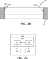
- the semiconductor cleaved bar 201 comprises a plurality of cleaved semiconductor structures 202 arranged next to each other. Further, as shown, each cleaved semiconductor structure 202 has a first facet 202A and a second facet 202B.
- the semiconductor bar 201 is treated as per the method 100 (described above), wherein the cleaved semiconductor structures 202 are stacked to dispose the first facet 202A and/or the second facet 202B to described exposure processes to enable uniform treatment of the cleaved semiconductor structures 202.
- the exposed first facet 202A can be heated at all times i.e., before, during, or after cleaning step and/or oxidation step.
- the cleaved semiconductor structure 202 provides the first facet 202A and the second facet 202B on opposing sides thereof. Further, the cleaved semiconductor structure 202 comprises a deposited passivating layer 230 (for example, group III atomic layer) deposited on each of the first and second facets 202A, 202B for protection from potential damage from COMD, corrosion, and the like.
- a deposited passivating layer 230 for example, group III atomic layer
- the cleaved semiconductor structure 202 comprises deposited first layers 232 on each of the first and second facets 202A, 202B for added protection from exposure to surroundings and thereby protecting the cleaved semiconductor structure 202 from damage effectively.
- the deposited first layers 232 are metallic coatings.
- the deposited first layers 232 are mirror coatings.
- the system 200 comprises an enclosure 204, and a pump 206 configured to generate vacuum condition (e.g., to ultra-high vacuum (UHV) level) inside the enclosure 204.
- the system 200 further comprises a laser heating source 208 mounted in the enclosure 204 to provide heat beam.
- the system 200 further comprises a fixture 210 adapted to mount the given structure 202 thereon in the enclosure 204, wherein the fixture 210 is configured to be manipulated to expose the first facet 202A (as shown in FIGs.
- the heat beam may be provided by the laser heating source 208 either before or after the cleaning and/ or oxidation process.
- the laser heating source 208 is a frontal irradiation source that is mounted externally to the enclosure 204.
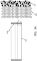
- the first facet 202A comprises the crystalline layer 228 thereon, wherein the crystalline layer 228 is formed via group III to group V atoms. Further, the first facet 202A has an amorphous oxide layer 302 contaminating the first facet 202A of the cleaved semiconductor structure 202.
- the first facet 202A of the cleaved semiconductor structure 202 is exposed to the cleaning beam from the cleaning source 214 by manipulating the fixture 210 to remove the amorphous oxide layer 302 thereof.
- a cleaning step removes the amorphous oxide layer 302 from the first facet 202A of the cleaved semiconductor structure 202 prior to further treatment in an a quick, accurate and efficient manner.
- FIG. 3B illustrated is a representative diagram of an exemplary cleaved semiconductor structure 202 after cleaning the first facet 202A of the cleaved semiconductor structure 202.
- the amorphous oxide layer 302 is removed from the first facet 202A of the cleaved semiconductor structure 202 and may thereafter be treated with other deposition or cleaning techniques as per requirement.
- FIG. 3C illustrated is a representative diagram of an exemplary cleaved semiconductor structure 202 after cleaning the first facet 202A of the cleaved semiconductor structure 202 and provided with an ordered oxide layer 236 formed thereon.
- the oxidizing source 218 is configured to form the ordered oxide layer 236 via controlled oxidation onto the crystalline layer 228 formed on the first facet 202A, wherein the fixture 210 is configured to be manipulated to expose the oxidation agent from the oxidizing source 218 to generate the ordered oxide layer 236.
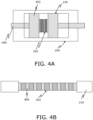
- FIG. 4A illustrated is a schematic diagram of an exemplary stacking fixture 234, in accordance with one or more embodiments of the present disclosure.
- the stacking fixture 234 is configured for holding or stacking the plurality of cleaved semiconductor structures 202 therein.
- the stacking fixture 234 comprises either screws or springs 400 configured to push the clamps 402 against each other, adding a suitable pressure to keep the plurality of semiconductor structures 202 "sandwiched" between the clamps 402.
- FIG. 4B illustrated is a detailed view of the exemplary fixture 210 holding the plurality of cleaved semiconductor structures 202.
- each of the plurality of cleaved semiconductor structures 202 is spaced apart by a spacing element 404 to isolate and protect the contacts of each of the cleaved semiconductor structures 202, so that contacts of two adjacent cleaved semiconductor structures 202 are not touching each other directly, as they could melt, etc.
- the spacing element 404 may be GaAs, Sapphire, and the like.
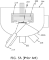
- FIG. 5A illustrated is a schematic diagram of a conventional heating method for heating the cleaved semiconductor structure 202.
- the cleaved semiconductor bar 201 comprising the plurality of the cleaved semiconductor structures 202 are mounted onto the fixture 210 inside in the enclosure 204 for further treatment therein.
- the cleaning source 214, the oxidizing source 218, and the deposition source are configured to treat the first facet 202A of the cleaved semiconductor structure from a first direction and the heating to be done by the conventional heating sources 208 was required to done from a direction opposite to the first direction i.e., opposite to the treated facet 202A of the cleaved semiconductor structure 202 such as, in existing semiconductor manufacturing processes, such as passivation, deposition, etc. wherein the semiconductor structure 202 is required to be heated from a direction opposite to a treated facet 202A of the cleaved semiconductor structure 202, as shown in FIG. 5A and thereby requires higher amounts of heat energy to be applied which consequently causes damage to the surfaces of the semiconductor structure 202 and results in a poor efficiency for the system 200 or method 100.
- FIG. 5B illustrated is a schematic diagram of a frontal heating-mechanism of the method 100 or system 200 for heating the cleaved semiconductor structure 202 surfaces to be utilized in semiconductor manufacturing processes, in accordance with one or more embodiments of the present disclosure.
- the method 100 or the system 200 of the present disclosure provides a novel frontal heating mechanism to overcome the aforementioned problems.
- the system 200 comprises the enclosure 204, and the pump 206 (not shown) configured to generate vacuum condition (e.g., to ultra-high vacuum (UHV) level) inside the enclosure 204.
- UHV ultra-high vacuum
- the system 200 further comprises a fixture 210 adapted to mount the given structure 202 thereon in the enclosure 204, wherein the fixture 210 is configured to be manipulated to expose the first facet 202A (as shown in FIGs. 2A and 2B ) and/or the second facet 202B (as shown in FIGs. 2A and 2B ) of the cleaved semiconductor structure 202 in the enclosure 208 to the heat beam from the laser heating source 208 by disposing the first facet 202A opposing the heating source 208.
- the heat beam may be provided by the laser heating source 208 either before or after the cleaning and/or oxidation process.
- the laser heating source 208 is a frontal irradiation source that is mounted externally to the enclosure 204.
- the cleaved semiconductor bar 201 comprising the plurality of the cleaved semiconductor structures 202 are mounted onto the fixture 210 inside in the enclosure 204 for further treatment therein.
- the laser heating source 208 is exposed to a given facet (such as, the first facet 202A) to heat the exposed facet 202A of the cleaved semiconductor structure 202 to aid with the above-described process.
- the system 200 further comprises a heating source 208 mounted in the enclosure 204 to provide heat beam for heating the exposed facet 202A of the cleaved semiconductor structure 202.
- the system 200 comprises a first port 212 configured for mounting the laser heating source 208 in the enclosure 204.
- the laser heating source 208 may be employed either before or after, or during, the cleaning and/or oxidation process.
- the laser heating source 208 is a frontal irradiation source, such as a laser, that is mounted externally to the enclosure 204. Therefore, the system 200 comprises a transparent viewport 221 (as shown in FIG.
- the system 200 comprises a beam shaper 223 (as shown in FIG. 5 ) to shape the heat beam from the heating source 222 to be directed (shaped accordingly) to the exposed facet of the cleaved semiconductor structure 202 mounted in the enclosure 204 (as discussed in detail in the proceeding paragraphs).
- the system 200 further comprises a second port 216 for mounting a cleaning source 214 in the enclosure 204, a third port 220 for mounting an oxidizing source 218 in the enclosure 204.
- the system 200 further comprises a fixture 210 adapted to mount the given structure 202 thereon in the enclosure 204, wherein the fixture 210 is configured to be manipulated to expose the first facet 202A (as shown in FIGs. 2A and 2B ) and/or the second facet 202B (as shown in FIGs.
- the system 200 further comprises a deposition source 222 mounted in the enclosure 204.
- the system 200 comprises a fourth port 224 for mounting the deposition source 222 in the enclosure 204.
- the fixture 210 is configured to be manipulated to expose, prior to exposing the first facet 202A to the oxidation agent from the oxidizing source 218, the first facet 202A of the cleaved semiconductor structure 202 in the enclosure 204 to group III atoms from the deposition source 222, by disposing the first facet 202A opposing the deposition source 222.
- the system 200 further comprises a monitoring equipment (not shown).
- the monitoring equipment is configured to be utilized to provide visibility for observation and/or monitoring of the surface of the cleaved semiconductor structure 202 in the enclosure 204.
- the system 200 further comprises a fifth port 226 in the form of a transparent viewport to allow the monitoring equipment, that is mounted externally, to be used to observe the cleaved semiconductor structure 202 inside the enclosure 204.
- FIG. 5C illustrated is a schematic diagram of a dual heating-mechanism of the method 100 or system 200 for heating the cleaved semiconductor structure 202 surface to be utilized in semiconductor manufacturing processes, in accordance with one or more embodiments of the present disclosure.
- FIG. 5C is to be read in conjunction with FIG. 5A and 5B .
- both facets 202A and 202B of the cleaved semiconductor structure 202 are treated simultaneously via the laser heating sources 208, 208'.
- there are two laser heating sources 208 (a first laser heating source), 208' (a second laser heating source) configured to heat both the facets 202A and 202B of the cleaved semiconductor simultaneously.
- a beam shaper for each laser heating source can be provided.
- a single chamber i.e., the enclosure is utilized, wherein both facets i.e., the first facet and the second facet, may be heated and further treated, cleaned, and passivated without employing any other chambers or leaving the enclosure to make the method faster and efficient to solve the aforementioned problems of FIG. 5A and consequently increasing the efficiency and throughput of the method 100 or the system 200.
- two cleaning sources 214, two oxidizing sources 218 and two deposition sources 222 may also be interchangeably utilized for an efficient semiconductor manufacturing process such as, passivation of the cleaved semiconductor structure 202.
- a graphical representation 600 of temperature variations inside the cleaved semiconductor structure 202 as a measure of distance from the exposed surface to the laser heating source in accordance with an embodiment of the present disclosure.
- the x-axis and the y-axis depict the distance (in millimetres) from the exposed surface to the heating source and the temperature (in degree Celsius), respectively.
- temperature follows an inverse relationship with distance, as the temperature decreases through the thickness of the semiconductor structure.
Landscapes
- Drying Of Semiconductors (AREA)
- Recrystallisation Techniques (AREA)
Priority Applications (2)
| Application Number | Priority Date | Filing Date | Title |
|---|---|---|---|
| EP22212690.6A EP4386821A1 (fr) | 2022-12-12 | 2022-12-12 | Procédé de chauffage d'une structure semi-conductrice |
| EP23214150.7A EP4391030A1 (fr) | 2022-12-12 | 2023-12-05 | Procédé de chauffage d'une structure semi-conductrice |
Applications Claiming Priority (1)
| Application Number | Priority Date | Filing Date | Title |
|---|---|---|---|
| EP22212690.6A EP4386821A1 (fr) | 2022-12-12 | 2022-12-12 | Procédé de chauffage d'une structure semi-conductrice |
Publications (1)
| Publication Number | Publication Date |
|---|---|
| EP4386821A1 true EP4386821A1 (fr) | 2024-06-19 |
Family
ID=84488846
Family Applications (2)
| Application Number | Title | Priority Date | Filing Date |
|---|---|---|---|
| EP22212690.6A Withdrawn EP4386821A1 (fr) | 2022-12-12 | 2022-12-12 | Procédé de chauffage d'une structure semi-conductrice |
| EP23214150.7A Pending EP4391030A1 (fr) | 2022-12-12 | 2023-12-05 | Procédé de chauffage d'une structure semi-conductrice |
Family Applications After (1)
| Application Number | Title | Priority Date | Filing Date |
|---|---|---|---|
| EP23214150.7A Pending EP4391030A1 (fr) | 2022-12-12 | 2023-12-05 | Procédé de chauffage d'une structure semi-conductrice |
Country Status (1)
| Country | Link |
|---|---|
| EP (2) | EP4386821A1 (fr) |
Citations (3)
| Publication number | Priority date | Publication date | Assignee | Title |
|---|---|---|---|---|
| US6242291B1 (en) * | 1996-12-12 | 2001-06-05 | Semiconductor Energy Laboratory Co., Ltd. | Laser annealing method and laser annealing device |
| US20160379851A1 (en) * | 2015-06-29 | 2016-12-29 | Bharath Swaminathan | Temperature controlled substrate processing |
| WO2017165550A1 (fr) * | 2016-03-22 | 2017-09-28 | Tokyo Electron Limited | Système et procédé permettant la régulation de température dans un système de traitement par plasma |
Family Cites Families (3)
| Publication number | Priority date | Publication date | Assignee | Title |
|---|---|---|---|---|
| US4475027A (en) * | 1981-11-17 | 1984-10-02 | Allied Corporation | Optical beam homogenizer |
| US4733944A (en) * | 1986-01-24 | 1988-03-29 | Xmr, Inc. | Optical beam integration system |
| US7232715B2 (en) * | 2002-11-15 | 2007-06-19 | Semiconductor Energy Laboratory Co., Ltd. | Method for fabricating semiconductor film and semiconductor device and laser processing apparatus |
-
2022
- 2022-12-12 EP EP22212690.6A patent/EP4386821A1/fr not_active Withdrawn
-
2023
- 2023-12-05 EP EP23214150.7A patent/EP4391030A1/fr active Pending
Patent Citations (3)
| Publication number | Priority date | Publication date | Assignee | Title |
|---|---|---|---|---|
| US6242291B1 (en) * | 1996-12-12 | 2001-06-05 | Semiconductor Energy Laboratory Co., Ltd. | Laser annealing method and laser annealing device |
| US20160379851A1 (en) * | 2015-06-29 | 2016-12-29 | Bharath Swaminathan | Temperature controlled substrate processing |
| WO2017165550A1 (fr) * | 2016-03-22 | 2017-09-28 | Tokyo Electron Limited | Système et procédé permettant la régulation de température dans un système de traitement par plasma |
Also Published As
| Publication number | Publication date |
|---|---|
| EP4391030A1 (fr) | 2024-06-26 |
Similar Documents
| Publication | Publication Date | Title |
|---|---|---|
| US8097543B2 (en) | Apparatus and method of aligning and positioning a cold substrate on a hot surface | |
| US12322656B2 (en) | Substrate laser processing method and substrate laser processing apparatus | |
| KR102742588B1 (ko) | 저부 처리 | |
| JP6563166B2 (ja) | Fibおよび/または電子顕微鏡とともに使用するデュアル・レーザ・ビーム・システム | |
| US8912075B1 (en) | Wafer edge warp supression for thin wafer supported by tape frame | |
| US10020204B2 (en) | Bottom processing | |
| US7947584B2 (en) | Suitably short wavelength light for laser annealing of silicon in DSA type systems | |
| US9117868B1 (en) | Bipolar electrostatic chuck for dicing tape thermal management during plasma dicing | |
| US9293304B2 (en) | Plasma thermal shield for heat dissipation in plasma chamber | |
| US7838431B2 (en) | Method for surface treatment of semiconductor substrates | |
| RU2401185C2 (ru) | Способ лазерной обработки и устройство обработки, основанные на обычных вызванных лазером изменениях материала | |
| US9112050B1 (en) | Dicing tape thermal management by wafer frame support ring cooling during plasma dicing | |
| WO2008080099A2 (fr) | Système optique laser | |
| KR20140022336A (ko) | 다중-펄스 버스트들을 갖는 펄스 트레인 레이저를 이용한 웨이퍼 다이싱 및 플라즈마 식각 | |
| EP4386821A1 (fr) | Procédé de chauffage d'une structure semi-conductrice | |
| EP4386823B1 (fr) | Procédé de passivation de structure semi-conductrice clivée | |
| JP2009527439A (ja) | 薄膜成長時の特性改変法 | |
| KR101124408B1 (ko) | 매립된 종의 선형 포커싱된 레이저-어닐링 | |
| KR20220035251A (ko) | 챔버 컴포넌트의 리세스를 보수하기 위한 방법들 | |
| JP2004289140A (ja) | レーザ照射装置及びレーザ照射方法並びに半導体装置の作製方法。 | |
| TW202423586A (zh) | 雷射光束成形和圖案化的雷射製造系統及其方法 | |
| Bäuerle | Lasers, experimental aspects, spatial confinement | |
| JPS63247719A (ja) | レ−ザ出力安定化方法 |
Legal Events
| Date | Code | Title | Description |
|---|---|---|---|
| PUAI | Public reference made under article 153(3) epc to a published international application that has entered the european phase |
Free format text: ORIGINAL CODE: 0009012 |
|
| STAA | Information on the status of an ep patent application or granted ep patent |
Free format text: STATUS: THE APPLICATION HAS BEEN PUBLISHED |
|
| AK | Designated contracting states |
Kind code of ref document: A1 Designated state(s): AL AT BE BG CH CY CZ DE DK EE ES FI FR GB GR HR HU IE IS IT LI LT LU LV MC ME MK MT NL NO PL PT RO RS SE SI SK SM TR |
|
| STAA | Information on the status of an ep patent application or granted ep patent |
Free format text: STATUS: THE APPLICATION IS DEEMED TO BE WITHDRAWN |
|
| 18D | Application deemed to be withdrawn |
Effective date: 20241220 |