EP4386845A1 - Substrat matriciel, panneau d'affichage et dispositif d'affichage - Google Patents
Substrat matriciel, panneau d'affichage et dispositif d'affichage Download PDFInfo
- Publication number
- EP4386845A1 EP4386845A1 EP22948874.7A EP22948874A EP4386845A1 EP 4386845 A1 EP4386845 A1 EP 4386845A1 EP 22948874 A EP22948874 A EP 22948874A EP 4386845 A1 EP4386845 A1 EP 4386845A1
- Authority
- EP
- European Patent Office
- Prior art keywords
- metal wire
- transistor
- metal
- initialization
- array substrate
- Prior art date
- Legal status (The legal status is an assumption and is not a legal conclusion. Google has not performed a legal analysis and makes no representation as to the accuracy of the status listed.)
- Pending
Links
Images















Classifications
-
- G—PHYSICS
- G09—EDUCATION; CRYPTOGRAPHY; DISPLAY; ADVERTISING; SEALS
- G09G—ARRANGEMENTS OR CIRCUITS FOR CONTROL OF INDICATING DEVICES USING STATIC MEANS TO PRESENT VARIABLE INFORMATION
- G09G3/00—Control arrangements or circuits, of interest only in connection with visual indicators other than cathode-ray tubes
- G09G3/20—Control arrangements or circuits, of interest only in connection with visual indicators other than cathode-ray tubes for presentation of an assembly of a number of characters, e.g. a page, by composing the assembly by combination of individual elements arranged in a matrix no fixed position being assigned to or needed to be assigned to the individual characters or partial characters
- G09G3/22—Control arrangements or circuits, of interest only in connection with visual indicators other than cathode-ray tubes for presentation of an assembly of a number of characters, e.g. a page, by composing the assembly by combination of individual elements arranged in a matrix no fixed position being assigned to or needed to be assigned to the individual characters or partial characters using controlled light sources
- G09G3/30—Control arrangements or circuits, of interest only in connection with visual indicators other than cathode-ray tubes for presentation of an assembly of a number of characters, e.g. a page, by composing the assembly by combination of individual elements arranged in a matrix no fixed position being assigned to or needed to be assigned to the individual characters or partial characters using controlled light sources using electroluminescent panels
- G09G3/32—Control arrangements or circuits, of interest only in connection with visual indicators other than cathode-ray tubes for presentation of an assembly of a number of characters, e.g. a page, by composing the assembly by combination of individual elements arranged in a matrix no fixed position being assigned to or needed to be assigned to the individual characters or partial characters using controlled light sources using electroluminescent panels semiconductive, e.g. using light-emitting diodes [LED]
-
- H—ELECTRICITY
- H10—SEMICONDUCTOR DEVICES; ELECTRIC SOLID-STATE DEVICES NOT OTHERWISE PROVIDED FOR
- H10D—INORGANIC ELECTRIC SEMICONDUCTOR DEVICES
- H10D86/00—Integrated devices formed in or on insulating or conducting substrates, e.g. formed in silicon-on-insulator [SOI] substrates or on stainless steel or glass substrates
- H10D86/40—Integrated devices formed in or on insulating or conducting substrates, e.g. formed in silicon-on-insulator [SOI] substrates or on stainless steel or glass substrates characterised by multiple TFTs
-
- G—PHYSICS
- G09—EDUCATION; CRYPTOGRAPHY; DISPLAY; ADVERTISING; SEALS
- G09G—ARRANGEMENTS OR CIRCUITS FOR CONTROL OF INDICATING DEVICES USING STATIC MEANS TO PRESENT VARIABLE INFORMATION
- G09G3/00—Control arrangements or circuits, of interest only in connection with visual indicators other than cathode-ray tubes
- G09G3/20—Control arrangements or circuits, of interest only in connection with visual indicators other than cathode-ray tubes for presentation of an assembly of a number of characters, e.g. a page, by composing the assembly by combination of individual elements arranged in a matrix no fixed position being assigned to or needed to be assigned to the individual characters or partial characters
- G09G3/22—Control arrangements or circuits, of interest only in connection with visual indicators other than cathode-ray tubes for presentation of an assembly of a number of characters, e.g. a page, by composing the assembly by combination of individual elements arranged in a matrix no fixed position being assigned to or needed to be assigned to the individual characters or partial characters using controlled light sources
- G09G3/30—Control arrangements or circuits, of interest only in connection with visual indicators other than cathode-ray tubes for presentation of an assembly of a number of characters, e.g. a page, by composing the assembly by combination of individual elements arranged in a matrix no fixed position being assigned to or needed to be assigned to the individual characters or partial characters using controlled light sources using electroluminescent panels
- G09G3/32—Control arrangements or circuits, of interest only in connection with visual indicators other than cathode-ray tubes for presentation of an assembly of a number of characters, e.g. a page, by composing the assembly by combination of individual elements arranged in a matrix no fixed position being assigned to or needed to be assigned to the individual characters or partial characters using controlled light sources using electroluminescent panels semiconductive, e.g. using light-emitting diodes [LED]
- G09G3/3208—Control arrangements or circuits, of interest only in connection with visual indicators other than cathode-ray tubes for presentation of an assembly of a number of characters, e.g. a page, by composing the assembly by combination of individual elements arranged in a matrix no fixed position being assigned to or needed to be assigned to the individual characters or partial characters using controlled light sources using electroluminescent panels semiconductive, e.g. using light-emitting diodes [LED] organic, e.g. using organic light-emitting diodes [OLED]
- G09G3/3225—Control arrangements or circuits, of interest only in connection with visual indicators other than cathode-ray tubes for presentation of an assembly of a number of characters, e.g. a page, by composing the assembly by combination of individual elements arranged in a matrix no fixed position being assigned to or needed to be assigned to the individual characters or partial characters using controlled light sources using electroluminescent panels semiconductive, e.g. using light-emitting diodes [LED] organic, e.g. using organic light-emitting diodes [OLED] using an active matrix
- G09G3/3233—Control arrangements or circuits, of interest only in connection with visual indicators other than cathode-ray tubes for presentation of an assembly of a number of characters, e.g. a page, by composing the assembly by combination of individual elements arranged in a matrix no fixed position being assigned to or needed to be assigned to the individual characters or partial characters using controlled light sources using electroluminescent panels semiconductive, e.g. using light-emitting diodes [LED] organic, e.g. using organic light-emitting diodes [OLED] using an active matrix with pixel circuitry controlling the current through the light-emitting element
-
- H—ELECTRICITY
- H10—SEMICONDUCTOR DEVICES; ELECTRIC SOLID-STATE DEVICES NOT OTHERWISE PROVIDED FOR
- H10D—INORGANIC ELECTRIC SEMICONDUCTOR DEVICES
- H10D86/00—Integrated devices formed in or on insulating or conducting substrates, e.g. formed in silicon-on-insulator [SOI] substrates or on stainless steel or glass substrates
- H10D86/40—Integrated devices formed in or on insulating or conducting substrates, e.g. formed in silicon-on-insulator [SOI] substrates or on stainless steel or glass substrates characterised by multiple TFTs
- H10D86/441—Interconnections, e.g. scanning lines
-
- H—ELECTRICITY
- H10—SEMICONDUCTOR DEVICES; ELECTRIC SOLID-STATE DEVICES NOT OTHERWISE PROVIDED FOR
- H10D—INORGANIC ELECTRIC SEMICONDUCTOR DEVICES
- H10D86/00—Integrated devices formed in or on insulating or conducting substrates, e.g. formed in silicon-on-insulator [SOI] substrates or on stainless steel or glass substrates
- H10D86/40—Integrated devices formed in or on insulating or conducting substrates, e.g. formed in silicon-on-insulator [SOI] substrates or on stainless steel or glass substrates characterised by multiple TFTs
- H10D86/60—Integrated devices formed in or on insulating or conducting substrates, e.g. formed in silicon-on-insulator [SOI] substrates or on stainless steel or glass substrates characterised by multiple TFTs wherein the TFTs are in active matrices
-
- H—ELECTRICITY
- H10—SEMICONDUCTOR DEVICES; ELECTRIC SOLID-STATE DEVICES NOT OTHERWISE PROVIDED FOR
- H10K—ORGANIC ELECTRIC SOLID-STATE DEVICES
- H10K59/00—Integrated devices, or assemblies of multiple devices, comprising at least one organic light-emitting element covered by group H10K50/00
- H10K59/10—OLED displays
- H10K59/12—Active-matrix OLED [AMOLED] displays
-
- H—ELECTRICITY
- H10—SEMICONDUCTOR DEVICES; ELECTRIC SOLID-STATE DEVICES NOT OTHERWISE PROVIDED FOR
- H10K—ORGANIC ELECTRIC SOLID-STATE DEVICES
- H10K59/00—Integrated devices, or assemblies of multiple devices, comprising at least one organic light-emitting element covered by group H10K50/00
- H10K59/10—OLED displays
- H10K59/12—Active-matrix OLED [AMOLED] displays
- H10K59/121—Active-matrix OLED [AMOLED] displays characterised by the geometry or disposition of pixel elements
- H10K59/1213—Active-matrix OLED [AMOLED] displays characterised by the geometry or disposition of pixel elements the pixel elements being TFTs
-
- H—ELECTRICITY
- H10—SEMICONDUCTOR DEVICES; ELECTRIC SOLID-STATE DEVICES NOT OTHERWISE PROVIDED FOR
- H10K—ORGANIC ELECTRIC SOLID-STATE DEVICES
- H10K59/00—Integrated devices, or assemblies of multiple devices, comprising at least one organic light-emitting element covered by group H10K50/00
- H10K59/10—OLED displays
- H10K59/12—Active-matrix OLED [AMOLED] displays
- H10K59/131—Interconnections, e.g. wiring lines or terminals
-
- G—PHYSICS
- G09—EDUCATION; CRYPTOGRAPHY; DISPLAY; ADVERTISING; SEALS
- G09G—ARRANGEMENTS OR CIRCUITS FOR CONTROL OF INDICATING DEVICES USING STATIC MEANS TO PRESENT VARIABLE INFORMATION
- G09G2300/00—Aspects of the constitution of display devices
- G09G2300/04—Structural and physical details of display devices
- G09G2300/0421—Structural details of the set of electrodes
- G09G2300/0426—Layout of electrodes and connections
-
- G—PHYSICS
- G09—EDUCATION; CRYPTOGRAPHY; DISPLAY; ADVERTISING; SEALS
- G09G—ARRANGEMENTS OR CIRCUITS FOR CONTROL OF INDICATING DEVICES USING STATIC MEANS TO PRESENT VARIABLE INFORMATION
- G09G2300/00—Aspects of the constitution of display devices
- G09G2300/08—Active matrix structure, i.e. with use of active elements, inclusive of non-linear two terminal elements, in the pixels together with light emitting or modulating elements
- G09G2300/0809—Several active elements per pixel in active matrix panels
-
- G—PHYSICS
- G09—EDUCATION; CRYPTOGRAPHY; DISPLAY; ADVERTISING; SEALS
- G09G—ARRANGEMENTS OR CIRCUITS FOR CONTROL OF INDICATING DEVICES USING STATIC MEANS TO PRESENT VARIABLE INFORMATION
- G09G2300/00—Aspects of the constitution of display devices
- G09G2300/08—Active matrix structure, i.e. with use of active elements, inclusive of non-linear two terminal elements, in the pixels together with light emitting or modulating elements
- G09G2300/0809—Several active elements per pixel in active matrix panels
- G09G2300/0814—Several active elements per pixel in active matrix panels used for selection purposes, e.g. logical AND for partial update
-
- G—PHYSICS
- G09—EDUCATION; CRYPTOGRAPHY; DISPLAY; ADVERTISING; SEALS
- G09G—ARRANGEMENTS OR CIRCUITS FOR CONTROL OF INDICATING DEVICES USING STATIC MEANS TO PRESENT VARIABLE INFORMATION
- G09G2300/00—Aspects of the constitution of display devices
- G09G2300/08—Active matrix structure, i.e. with use of active elements, inclusive of non-linear two terminal elements, in the pixels together with light emitting or modulating elements
- G09G2300/0809—Several active elements per pixel in active matrix panels
- G09G2300/0819—Several active elements per pixel in active matrix panels used for counteracting undesired variations, e.g. feedback or autozeroing
-
- G—PHYSICS
- G09—EDUCATION; CRYPTOGRAPHY; DISPLAY; ADVERTISING; SEALS
- G09G—ARRANGEMENTS OR CIRCUITS FOR CONTROL OF INDICATING DEVICES USING STATIC MEANS TO PRESENT VARIABLE INFORMATION
- G09G2300/00—Aspects of the constitution of display devices
- G09G2300/08—Active matrix structure, i.e. with use of active elements, inclusive of non-linear two terminal elements, in the pixels together with light emitting or modulating elements
- G09G2300/0809—Several active elements per pixel in active matrix panels
- G09G2300/0842—Several active elements per pixel in active matrix panels forming a memory circuit, e.g. a dynamic memory with one capacitor
- G09G2300/0861—Several active elements per pixel in active matrix panels forming a memory circuit, e.g. a dynamic memory with one capacitor with additional control of the display period without amending the charge stored in a pixel memory, e.g. by means of additional select electrodes
-
- G—PHYSICS
- G09—EDUCATION; CRYPTOGRAPHY; DISPLAY; ADVERTISING; SEALS
- G09G—ARRANGEMENTS OR CIRCUITS FOR CONTROL OF INDICATING DEVICES USING STATIC MEANS TO PRESENT VARIABLE INFORMATION
- G09G2300/00—Aspects of the constitution of display devices
- G09G2300/08—Active matrix structure, i.e. with use of active elements, inclusive of non-linear two terminal elements, in the pixels together with light emitting or modulating elements
- G09G2300/0809—Several active elements per pixel in active matrix panels
- G09G2300/0842—Several active elements per pixel in active matrix panels forming a memory circuit, e.g. a dynamic memory with one capacitor
- G09G2300/0861—Several active elements per pixel in active matrix panels forming a memory circuit, e.g. a dynamic memory with one capacitor with additional control of the display period without amending the charge stored in a pixel memory, e.g. by means of additional select electrodes
- G09G2300/0866—Several active elements per pixel in active matrix panels forming a memory circuit, e.g. a dynamic memory with one capacitor with additional control of the display period without amending the charge stored in a pixel memory, e.g. by means of additional select electrodes by means of changes in the pixel supply voltage
-
- G—PHYSICS
- G09—EDUCATION; CRYPTOGRAPHY; DISPLAY; ADVERTISING; SEALS
- G09G—ARRANGEMENTS OR CIRCUITS FOR CONTROL OF INDICATING DEVICES USING STATIC MEANS TO PRESENT VARIABLE INFORMATION
- G09G2310/00—Command of the display device
- G09G2310/08—Details of timing specific for flat panels, other than clock recovery
-
- G—PHYSICS
- G09—EDUCATION; CRYPTOGRAPHY; DISPLAY; ADVERTISING; SEALS
- G09G—ARRANGEMENTS OR CIRCUITS FOR CONTROL OF INDICATING DEVICES USING STATIC MEANS TO PRESENT VARIABLE INFORMATION
- G09G2320/00—Control of display operating conditions
- G09G2320/02—Improving the quality of display appearance
- G09G2320/0233—Improving the luminance or brightness uniformity across the screen
Definitions
- the present application relates to a field of display technology, for example, an array substrate, a display panel, and a display device.
- pixel circuits in display panels have a common problem of leakage, which causes a change in display brightness, making it easy for human eyes to recognize abnormalities in the display picture and affecting the display effect of the display devices.
- the present application provides an array substrate, a display panel and a display device to improve the display effect of a display picture.
- an array substrate includes a substrate, an active layer, multiple metal layers and multiple pixel circuits.
- the active layer and the multiple metal layers are stacked on one side of the substrate.
- the multiple pixel circuits are formed on the array substrate and a pixel circuit of the multiple pixel circuits includes a drive transistor, a first initialization transistor, and a second initialization transistor.
- the multiple metal layers at least include a first metal wire extending in a first direction and a second metal wire extending in a second direction.
- the first metal wire and the second metal wire are located in different layers.
- the first initialization transistor is connected between the first metal wire and a gate of the drive transistor and is configured to transmit a first initialization voltage on the first metal wire to the gate of the drive transistor.
- the second initialization transistor is connected between the second metal wire and a light-emitting element and is configured to transmit a second initialization voltage on the second metal wire to the light-emitting element.
- the first direction and the second direction intersect and are perpendicular to the direction of the thickness of the array substrate, respectively.
- a display panel is provided and includes the array substrate provided by any embodiment of the present application.
- a display device is provided and includes the display panel provided by any embodiment of the present application.
- an active layer and multiple metal layers are stacked on a substrate.
- the multiple metal layers at least include a first metal wire extending in a first direction and a second metal wire extending in a second direction.
- the first metal wire and the second metal wire are located in different layers.
- a first initialization transistor is connected between the first metal wire and a gate of a drive transistor and is configured to transmit a first initialization voltage on the first metal wire to the gate of the drive transistor.
- a second initialization transistor is connected between the second metal wire and a light-emitting element and is configured to transmit a second initialization voltage on the second metal wire to the light-emitting element.
- the first metal wire and the second metal wire are configured in different layers so that corresponding initialization voltages can be provided to the first initialization transistor and the second initialization transistor to adjust the potential state of the gate of the drive transistor and of the anode of the light-emitting element. In this manner, the stability of the drive current is enhanced, and the uniformity of display brightness and display color cast are improved. Additionally, the first metal wire and the second metal wire are configured in different layers in a limited layout space so that the layout space utilization can be enhanced, the layout structure can be optimized, and the display PPI can be improved.
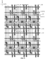
- FIG. 1 is a top view illustrating the structure of an array substrate according to an embodiment of the present application.
- FIG. 2 is a schematic diagram illustrating the sectional structure of an array substrate according to an embodiment of the present application.
- FIG. 2 may illustrate a sectional structure obtained by cutting the array substrate in FIG. 1 along the section line AA'.
- FIG. 3 is a schematic diagram illustrating the structure of a pixel circuit according to an embodiment of the present application.
- an array substrate provided by this embodiment of the present application includes a substrate 21, an active layer 10, and multiple metal layers; the active layer 10 and the multiple metal layers are stacked on one side of the substrate 21, and multiple pixel circuits are formed on the array substrate and a pixel circuit of multiple pixel circuits includes a drive transistor T1, a first initialization transistor T2, and a second initialization transistor T3.
- the multiple metal layers at least include a first metal wire 11 extending in a first direction and a second metal wire 12 extending in a second direction.
- the first metal wire 11 and the second metal wire 12 are located in different layers.
- the first initialization transistor T2 is connected between the first metal wire 11 and a gate of the drive transistor T1 and is configured to transmit a first initialization voltage Vrefl on the first metal wire 11 to the gate of the drive transistor T1.
- the second initialization transistor T3 is connected between the second metal wire 12 and a light-emitting element D1 and is configured to transmit a second initialization voltage Vref2 on the second metal wire 12 to the light-emitting element D1.
- the first direction and the second direction intersect and are perpendicular to the direction of the thickness of the array substrate, respectively.
- the first initialization transistor T2 is connected between the first metal wire 11 and the gate of the drive transistor T1, which can be understood that one electrode of the source or drain of the first initialization transistor T2 is electrically connected to the first metal wire 11 and that the other electrode of the source or drain of the first initialization transistor T2 is electrically connected to the gate of the drive transistor T1.
- the second initialization transistor T3 is connected between the second metal wire 12 and the light-emitting element D1, which can be understood that one electrode of the source or drain of the second initialization transistor T3 is electrically connected to the second metal wire 12 and that the other electrode of the source or the drain of the second initialization transistor T3 is electrically connected to the light-emitting element D1.
- the electrical connection may be a direct connection or an indirect connection.
- the substrate 21 may be used for providing protection and support for the array substrate.
- the substrate 21 may be a flexible substrate made of a material such as polyimide (PI), Polyethylene Naphthalate Two Formic Acid Glycol Ester (PEN), or Polyethylene terephthalate (PET) or may be a hard substrate made of a material such as glass.
- PI polyimide
- PEN Polyethylene Naphthalate Two Formic Acid Glycol Ester
- PET Polyethylene terephthalate
- the active layer 10 and multiple metal layers are sequentially disposed on one side of the substrate 21.
- the multiple metal layers are isolated from each other by an insulation layer.
- the multiple metal layers include a first metal layer M1, a second metal layer M2, and a third metal layer M3.
- a first interlayer insulation layer 22 is disposed between the active layer 10 and the first metal layer M1.
- a second interlayer insulation layer 23 is disposed between the first metal layer M1 and the second metal layer M2.
- a third interlayer insulation layer 24 is disposed between the second metal layer M2 and the third metal layer M3.
- a fourth interlayer insulation layer 25 is also disposed on a side of the third metal layer M3 away from the substrate 21.
- the active layer 10 may be made of polysilicon, metal oxide, and other materials.
- a pixel circuit is composed of at least a thin-film transistor.
- the thin-film transistor at least includes a drive transistor T1, a first initialization transistor T2, and a second initialization transistor T3.
- the first initialization transistor T2 is configured to initialize the gate potential of the drive transistor T1.
- the second initialization transistor T3 is configured to initialize the anode potential of the light-emitting element D1.
- the data voltage on a data line Data is written into the gate of the drive transistor T1 through a data writing transistor T4, the drive transistor T1, and a threshold compensation transistor T5 and is stored on a storage voltage Cst, thereby achieving functions of data writing and threshold compensation.
- the drive transistor T1 When a first light-emitting control transistor T6 and a second light-emitting control transistor T7 are turned on, the drive transistor T1 generates a drive current to drive the light-emitting element D1 to emit light.
- the first initialization voltage Vrefl is provided by the first metal wire 11, and the second initialization voltage Vref2 is provided by the second metal wire 12.
- the first metal wire 11 extends in the first direction.
- the second metal wire 12 extends in the second direction.
- the first direction may be the Y direction
- the second direction may be the X direction
- both the X direction and the Y direction are perpendicular to the direction of the thickness of the array substrate (that is, the Z direction).
- the first metal wire 11 and the second metal wire 12 are separately formed by mental materials in different layers of the multiple metal layers.
- the first metal wire 11 is located at the third metal layer M3, and the second metal wire 12 is located at the second metal layer M2.
- the first metal wire 11 transmits the first initialization voltage Vrefl to the first initialization transistor T2.
- the second metal wire 12 transmits the second initialization voltage Vref2 to the second initialization transistor T3.
- the first metal wire 11 and the second metal wire 12 are configured in different layers so that the corresponding initialization voltages can be supplied to the gate of the drive transistor T1 and the anode of the light-emitting element D1 to enhance the threshold compensation effect on the drive transistor T1, increase the uniformity of the drive current, and reduce the effect of the parasitic capacitance of the light-emitting element D1 on the drive current to reduce color cast. Meanwhile, it is also possible to optimize the layout structure, which helps improve the space utilization rate of the layout and the display pixels per inch (PPI).
- the initialization voltage supplied by the first metal wire 11 to the gate of the drive transistor T1 may be same as the initialization voltage supplied by the second metal wire 12 to the anode of the light-emitting element D1.
- the pixel circuit is controlled by the drive timing to enhance the threshold compensation effect on the drive transistor T1, increase the uniformity of the drive current, and reduce the effect of the parasitic capacitance of the light-emitting element D1 on the drive current to reduce color cast.
- the specific working principle thereof is to be described in the following embodiments:
- an active layer and multiple metal layers are stacked on a substrate.
- the multiple metal layers at least include a first metal wire extending in a first direction and a second metal wire extending in a second direction.
- the first metal wire and the second metal wire are located in different layers.
- a first initialization transistor is connected between the first metal wire and a gate of a drive transistor and is configured to transmit a first initialization voltage on the first metal wire to the gate of the drive transistor.
- a second initialization transistor is connected between the second metal wire and a light-emitting element and is configured to transmit a second initialization voltage on the second metal wire to the light-emitting element.
- the first metal wire and the second metal wire are configured in different layers so that corresponding initialization voltages can be provided to the first initialization transistor and the second initialization transistor to adjust the potential state of the gate of the drive transistor and of the anode of the light-emitting element.
- the stability of the drive current is enhanced, and the uniformity of display brightness and display color cast are improved.
- the first metal wire and the second metal wire are configured in different layers in a limited layout space so that the layout space utilization can be enhanced, the layout structure can be optimized, and the display PPI can be improved.
- the first metal wire 11 includes multiple first sub-metal wires 111 and multiple second sub-metal wires 112 that are arranged in multiple columns; each of the multiple first sub-metal wires 111 is disposed in a column, and part of the multiple second sub-metal wires 112 are arranged in a column; the first initialization transistor T2 is connected between corresponding one of the multiple first sub-metal wires 111 and the gate of the drive transistor T1; the second initialization transistor T3 is connected to corresponding one of the multiple second sub-metal wires 112.
- the multiple metal layers also include a third metal wire 13 and a fourth metal wire 14, which are a first scan line and a second scan line, respectively.
- the third metal wire 13 and the fourth metal wire 14 separately extend in the second direction.
- the orthographic projection of the second metal wire 12 on the substrate 21 is located between the orthographic projection of the third metal wire 13 on the substrate 21 and the orthographic projection of the fourth metal wire 14 on the substrate 21.
- the third metal wire 13 and the fourth metal wire 14 may both be located on the first metal layer.
- the third metal wire 13 overlaps the active layer 10 to form the first initialization transistor T2.
- the fourth metal wire 14 overlaps the active layer 10 to form the second initialization transistor T3.
- the transistor formed by the overlap of the third metal wire 13 and the active layer 10 is configured as a second initialization transistor T3 in the previous row of pixel circuits adjacent to the current row of pixel circuits.
- a single first sub-metal wire 111 is arranged in a column in the first direction, multiple second sub-metal wires 112 are arranged in a column in the first direction, and the multiple first sub-metal wires 111 and the multiple second sub-metal wires 112 are insulated from each other.
- a first terminal of the first initialization transistor T2 is connected to the first sub-metal wire 111.
- a second terminal of the first initialization transistor T2 is connected to the gate of the drive transistor T1.
- the first sub-metal wire 111 is configured to supply the first initialization voltage Vrefl to the first initialization transistor T2.
- a first terminal of the second initialization transistor T3 is connected to a first terminal of the second sub-metal wire 112.
- a second terminal of the second sub-metal wire 112 is connected to the second metal wire 12.
- a second terminal of the second initialization transistor T3 is connected to the anode of the light-emitting element D1.
- the second sub-metal wire 112 serves as a connection to transmit the second initialization voltage Vref2 provided by the second metal wire 12 to the first terminal of the second initialization transistor T3.
- the first initialization voltage Vrefl on the first metal wire 11 and the second initialization voltage Vref2 on the second metal wire 12 may be different.
- the first initialization voltage Vrefl in this embodiment may be smaller than the second initialization voltage Vref2. Since the first initialization voltage Vrefl is smaller, it is possible to pull the gate voltage of the drive transistor T1 to a lower potential so that the gate potential of the drive transistor T1 is completely reset. For different pixel circuits, it is possible to ensure that the data voltage can be completely written into the gate of the drive transistor T1, thereby enhancing the threshold compensation effect on the drive transistor T1, improving the uniformity of the drive current, and improving residual shadows.
- the second initialization voltage Vref2 is appropriately increased so that the effect of the parasitic capacitance of the light-emitting element D1 on the drive current can be reduced, and then the color cast caused by brightness deviation can be reduced.
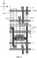
- FIG. 4 is a top view illustrating the structure of another array substrate according to an embodiment of the present application, specifically illustrating a partial structure of an array pixel circuit.
- the first sub-metal wire 111 extends in the Y direction and is connected to the first sub-metal wire 111 of the pixel circuits corresponding to the upper and lower rows to form a vertical line.
- Each first sub-metal wire 111 is arranged in a column.
- the second metal wire 12 extends in the X direction and is connected to the second metal wire 12 of the pixel circuits corresponding to the left and right columns to form a horizontal line.
- the second sub-metal wire 112 extends in the Y direction and is connected to the second metal wire 12 and connected to the second initialization transistor T3 via the active layer 10. Thus, multiple second sub-metal wires 112 are arranged in a column. The specific structure of a single pixel circuit is shown in the dashed box.
- the third metal wire 13 or the fourth metal wire 14 corresponding to the pixel circuits in two adjacent rows may be shared. That is, the fourth metal wire 14 corresponding to a pixel circuit in an nth row may be reused as the third metal wire 13 corresponding to a pixel circuit in an (n + 1)th row, where n is an integer greater than or equal to 1.
- the fourth metal wire 14 of a pixel circuit in an nth row is reused as the third metal wire 13 of a pixel circuit in an (n + 1)th row. That is, the second scan line in an nth row is used as the first scan line in an (n + 1)th row, which saves layout space and results in a higher PPI.
- FIG. 5 is a schematic diagram illustrating the structure of another pixel circuit according to an embodiment of the present application.
- a pixel circuit of the multiple pixel circuits also includes a first leakage compensation transistor T8 and a second leakage compensation transistor T9, the first leakage compensation transistor T8 is connected between the gate of the drive transistor T1 and a second electrode of the second leakage compensation transistor T9, and a first electrode of the second leakage compensation transistor T9 is connected to the first initialization transistor T2.
- a gate of the first leakage compensation transistor T8 and a gate of the second leakage compensation transistor T9 are connected to the same scan line and are configured to turn off the leakage path of the drive transistor T1 when the data writing is completed so as to reduce the leakage current and maintain the stability of the gate potential of drive transistor T1.
- the pixel circuit of the multiple pixel circuits also includes a first storage capacitor C1; the first storage capacitor C1 is connected to the second electrode of the second leakage compensation transistor T9 and is configured to store the potential of the second electrode of the second leakage compensation transistor T9.
- the parasitic capacitance between the gate of the first leakage compensation transistor T8 and the gate of the drive transistor T1 is coupled, and couples the gate potential of the drive transistor T1 so that the gate potential of the drive transistor T1 is similar to the first electrode potential of the first leakage compensation transistor T8 (the gate of the drive transistor T1 is connected to the second electrode of the first leakage compensation transistor T8, and the first electrode of the first leakage compensation transistor T8 is connected to the second electrode of the second leakage compensation transistor T9). Therefore, the voltage difference between the first electrode and the second electrode of the first leakage compensation transistor T8 is smaller so that the leakage current of the first leakage compensation transistor T8 is smaller, which helps maintain the stability of the gate potential of drive transistor T1.
- FIG. 6 is a top view illustrating the structure of another array substrate according to an embodiment of the present application.
- a second storage capacitor C2 is not shown in FIG. 6 .
- the multiple metal layers include a first metal layer M1, a second metal layer M2, and a third metal layer M3; the first metal layer M1 includes the gate of the drive transistor T1, the third metal wire 13, and the fourth metal wire 14, the second metal layer M2 includes the second metal wire 12, and the third metal layer M3 includes the first metal wire 11.
- the multiple metal layers also include a fifth metal wire 15 serving as a third scan line EMB.
- the fifth metal wire 15 is not disposed in the same layer as the first metal wire 11 and the second metal wire 12.
- the fifth metal wire 15 is located at the first metal layer M1.
- the orthographic projection of the fifth metal wire 15 on the substrate is located on one side of the orthographic projection of the second metal wire 12 on the substrate and does not overlap the orthographic projection of the second metal wire 12 on the substrate, that is, the orthographic projection of the fifth metal wire 15 on the substrate is staggered with the orthographic projection of the second metal wire 12 on the substrate.
- the fifth metal wire 15 overlaps the active layer 10 to form the first leakage compensation transistor T8 and the second leakage compensation transistor T9.
- the second metal wire 12 is connected to the first storage capacitor C1 that may be formed by the overlap of the second metal wire 12 and the active layer 10, which helps save layout space.
- the multiple metal layers also include a sixth metal wire 16 extending in the second direction and a seventh metal wire 17 extending in the second direction, and the sixth metal wire 16 and the seventh metal wire 17 are a fourth scan line S3 and a fifth scan line Em, respectively.
- the sixth metal wire 16 overlaps the active layer 10 to form a data writing transistor T4 and a threshold compensation transistor T5.
- the seventh metal wire 17 overlaps the active layer 10 to form a first light-emitting control transistor T6 and a second light-emitting control transistor T7.
- the active layer 10 overlapping the sixth metal wire 16 to form the data writing transistor T4 is connected to the data line Data through a via.
- the active layer 10 overlapping the seventh metal wire 17 to form the first light-emitting control transistor T6 is connected to a first power supply line VDD through a via (a second power supply line VSS is not shown in the figure).
- FIG. 7 is a top view illustrating the structure of another array substrate according to an embodiment of the present application. Based on the preceding multiple technical solutions, reference is made to FIG. 7 .
- the multiple second sub-metal wires 112 and the multiple first sub-metal wires 111 are connected to form a mesh. That is, the multiple first sub-metal wires 111 and the multiple second sub-metal wires 112 are connected together. Since the second sub-metal wire 112 is also connected to the second metal wire 12, the first metal wire 11 and the second metal wire 12 are connected to each other form a horizontal and vertical mesh structure.
- the first initialization voltage Vrefl is equal to the second initialization voltage Vrefl, that is, the second initialization voltage Vref2 may also be used as the first initialization voltage Vrefl.
- FIG. 8 is a top view illustrating the structure of another array substrate according to an embodiment of the present application.
- a first terminal of the first metal wire 11 is connected to the second metal wire 12
- a second terminal of the first metal wire 11 is connected to the first initialization transistor T2 and the second initialization transistor T3.
- the layout structure shown in FIG. 8 does not have a first sub-metal wire 111.
- the second metal wire 12 is connected to the first initialization transistor T2 and the second initialization transistor T3 via the first metal wire 11, that is, the first initialization transistor T2 and the second initialization transistor T3 are indirectly connected to the second metal wire 12 via the first metal wire 11, and the second initialization voltage Vref2 on the second metal wire 12 is transmitted to the gate of the drive transistor T1 and the anode of the light-emitting element D1 via the first initialization transistor T2 and the second initialization transistor T3, respectively.
- the second initialization voltage Vref2 is the first initialization voltage Vrefl.
- no vertical line first sub-metal wire 111
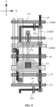
- FIG. 9 is a top view illustrating the structure of another array substrate according to an embodiment of the present application.
- the layout structure shown in FIG. 9 differs from the layout structure shown in FIG. 8 in that the structure of active layer 10 is different.
- the second leakage compensation transistor T9 is formed on the left side of the first leakage compensation transistor T8.
- the third metal wire 13 includes a first body portion 131 and a first branch portion 132.
- the fourth metal wire 14 includes a second body portion 141 and a second branch portion 142.
- the first body portion 131 and the second body portion 141 extend in the second direction.
- the first branch portion 132 and the second branch portion 142 extend in the first direction.
- the active layer 10 forming the second leakage compensation transistor T9 extends upward in the first direction and then extends in the second direction to overlap the first branch portion 132 of the third metal wire 13 to form the first initialization transistor T2.
- the first body portion 131 of the third metal wire 13 overlaps the active layer 10 to form the second initialization transistor T3 of the pixel circuit in the previous row.
- the second body portion 141 of the fourth metal wire 14 overlaps the active layer 10 extending in the first direction to form the second initialization transistor T3 of the pixel circuit in the current row.
- the second branch portion 142 of the fourth metal wire 14 overlaps the active layer 10 extending in the second direction to form the first initialization transistor T2 of the pixel circuit in the next row.
- the orthographic projection of the second metal wire 12 on the substrate 21 is located between the orthographic projection of the fifth metal wire 15 on the substrate 21 and the orthographic projection of the sixth metal wire 16 on the substrate 21, and the fifth metal wire 15 is located on a side of the second metal wire 12 facing away from the drive transistor T1.
- FIG. 10 is a drive timing waveform diagram of a pixel circuit according to an embodiment of the present application.
- FIG. 11 is a drive timing waveform diagram of another pixel circuit according to an embodiment of the present application, which is applicable to the pixel circuit shown in FIG. 5 .
- FIG. 11 specifically shows the drive timing of a black frame insertion stage.
- this embodiment is only described by using an example where multiple transistors are P-type transistors. In other embodiments, the multiple transistors may be N-type transistors.
- the working process of the pixel circuit provided by this embodiment of the present application includes at least an initialization stage 11, a data writing stage t2, a voltage normalization stage t3, a light-emitting stage t4, and a black frame insertion stage t5.
- a first scan signal transmitted on the first scan line S1 is a low level
- a second scan signal transmitted on the second scan line S2 is a high level
- a third scan signal transmitted on the third scan line EMB is a low level
- a fourth scan signal transmitted on the fourth scan line S3 is a high level
- a fifth scan signal transmitted on the fifth scan line EM is a high level. Therefore, the first initialization transistor T2, the first leakage compensation transistor T8, and the second leakage compensation transistor T9 are turned on, and the first initialization voltage Vrefl is transmitted to the gate of the drive transistor T1 to initialize the gate potential of the drive transistor T1.
- a first scan signal transmitted on the first scan line S1 is a high level
- a second scan signal transmitted on the second scan line S2 is a low level
- a third scan signal transmitted on the third scan line EMB is a low level
- a fourth scan signal transmitted on the fourth scan line S3 is a low level
- a fifth scan signal transmitted on the fifth scan line EM is a high level. Therefore, the data writing transistor T4, the threshold compensation transistor T5, the second initialization transistor T3, the first leakage compensation transistor T8, and the second leakage compensation transistor T9 are turned on, and the data voltage on the data line Data is written into the gate of the drive transistor T1.
- the drive transistor T1 When the gate voltage of drive transistor T1 reaches (Vdata + Vth), the drive transistor T1 is turned off, and the voltage is stored on the first storage capacitor C1 and the second storage capacitor C2, where Vdata is the data voltage, and Vth is the threshold voltage of the drive transistor. Meanwhile, the second initialization voltage Vref2 is written into the anode of the light-emitting element D1 via the second initialization transistor T3 to initialize the anode potential of the light-emitting element D1. At this time, the gate voltage of the drive transistor T1 is not equal to the storage voltage on the first storage capacitor C1.
- the third scan signal transmitted on the third scan line EMB jumps from a low level to a high level, and under the coupling effect of the parasitic capacitance of the gate of the drive transistor T1, the gate voltage of the drive transistor T1 is pulled up to be close to the voltage stored on the first storage capacitor C1 so that the voltage difference between the first electrode and the second electrode of the first leakage compensation transistor T8 is smaller.
- the leakage current of the first leakage compensation transistor T8 is smaller, and the gate voltage of the drive transistor T1 can be maintained stable.
- the first scan signal transmitted on the first scan line S1 is a high level
- the second scan signal transmitted on the second scan line S2 is a high level
- the third scan signal transmitted on the third scan line EMB is a high level
- the fourth scan signal transmitted on the fourth scan line S3 is a high level
- the fifth scan signal transmitted on the fifth scan line EM is a low level. Therefore, the first light-emitting control transistor T6 and the second light-emitting control transistor T7 are turned on, and the drive transistor T1 generates a drive current to drive the light-emitting element D1 to emit light. Since the gate voltage of drive transistor T1 can be maintained stable for a long time, the uniformity of the drive current can be ensured, and the residual shadows of display pictures can be improved.
- the pixel circuit When the fifth scan signal transmitted on the fifth scan line EM jumps from a low level to a high level, the pixel circuit enters the black frame insertion stage t5.
- the third scan signal transmitted on the third scan line EMB is always a high level, and the first leakage compensation transistor T8 and the second leakage compensation transistor T9 are in an off state.
- the fourth scan signal transmitted on the fourth scan line S3 maintains a high level, and the low level of the first scan signal transmitted on the first scan line S1 and the low level of the second scan signal transmitted on the second scan line S2 arrive successively. Since the first leakage compensation transistor T8 and the second leakage compensation transistor T9 are in the off state, the first initialization voltage Vrefl is not written into the gate of the drive transistor T1, and only the second initialization voltage Vref2 is written into the anode of the light-emitting element D 1 to reset the anode potential of the light-emitting element D 1.
- the fifth scan signal transmitted on the fifth scan line EM jumps from a high level to a low level, and the light-emitting element D1 continues to emit light.
- the black frame insertion stage may be performed multiple times; the black frame insertion stage is configured and the anode potential of the light-emitting element D1 is reset at the black frame insertion stage so that a low-frequency brightness component that is easily perceived by human eyes can be completely converted into a high-frequency brightness component that is not easily perceived, thereby improving the flickering of the display pictures.
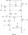
- FIG. 12 is a schematic diagram illustrating the structure of another pixel circuit according to an embodiment of the present application.
- a pixel circuit of the multiple pixel circuits also includes a first voltage writing control transistor T10, the first voltage writing control transistor T10 and the data writing transistor T4 are connected in series between the data line Data and the first electrode of the drive transistor T1, and a gate of the first voltage writing control transistor T10 is connected to the third scan signal transmitted on the third scan line EMB.
- the pixel circuit shown in FIG. 12 may be driven using the drive timing shown in FIG. 11 .
- the fourth scan signal transmitted on the fourth scan line S3 and the second scan signal transmitted on the second scan line S2 may be configured to be the same so that the fourth scan signal transmitted on the fourth scan line S3 also has a pulse within the black frame insertion stage t5.
- the scan frequency of the fourth scan signal transmitted on the fourth scan line S3 is increased.
- the scan frequency of the scan signal connected to the gate of the data writing transistor T4, the scan frequency of the scan signal connected to a gate of the first initialization transistor T2, and the scan frequency of the scan signal connected to a gate of the second initialization transistor T3 are all higher than a preset high scan frequency.
- the preset high scan frequency may be 60 Hz, and signals whose scan frequency is higher than the preset high scan frequency are high frequency signals.
- the scan signals on the first scan line S1, the second scan line S2, and the fourth scan line S3 are high frequency signals.
- the preset high scan frequency may also be 75 Hz, 100 Hz, or 120 Hz, which is not specifically limited in this embodiment.
- the first voltage writing control transistor T10 is turned off, even if the threshold compensation transistor T5 and the data writing transistor T4 are turned on in response to the fourth scan signal, the voltage of the first electrode of the first leakage compensation transistor T8 does not change greatly, and a smaller voltage difference can still be maintained between the second electrode and the first electrode of the first leakage compensation transistor T8. Therefore, the first leakage compensation transistor T8 can maintain a low leakage current.
- the fourth scan signal transmitted on the fourth scan line S3, the first scan signal transmitted on the first scan line S1, and the second scan signal transmitted on the second scan line S2 are all high frequency signals
- the first scan signal, the second scan signal, and the fourth scan signal may be generated by the same set of gate drive circuits, which facilitates a narrow frame design.
- FIG. 13 is a drive timing waveform diagram of another pixel circuit according to an embodiment of the present application.
- FIG. 14 is a drive timing waveform diagram of another pixel circuit according to an embodiment of the present application, which specifically illustrates the drive timing of the black frame insertion stage.
- the drive timings shown in FIGS. 13 and 14 are applicable to the pixel circuit shown in FIG. 12 .
- the working process of the pixel circuit includes stages described below.
- a first scan signal transmitted on the first scan line S1 is a low level
- a second scan signal transmitted on the second scan line S2 is a high level
- a third scan signal transmitted on the third scan line EMB is a low level
- a fourth scan signal transmitted on the fourth scan line S3 is a high level
- a fifth scan signal transmitted on the fifth scan line EM is a high level. Therefore, the first initialization transistor T2, the first leakage compensation transistor T8, and the second leakage compensation transistor T9 are turned on, and the first initialization voltage Vrefl is transmitted to the gate of the drive transistor T1 to initialize the gate potential of the drive transistor T1.
- a first scan signal transmitted on the first scan line S1 is a high level
- a second scan signal transmitted on the second scan line S2 is a low level
- a third scan signal transmitted on the third scan line EMB is a low level
- a fourth scan signal transmitted on the fourth scan line S3 is a low level
- a fifth scan signal transmitted on the fifth scan line EM is a high level. Therefore, the data writing transistor T4, the threshold compensation transistor T5, the second initialization transistor T3, the first voltage writing control transistor T10, the first leakage compensation transistor T8, and the second leakage compensation transistor T9 are turned on, and a voltage related to the data voltage on the data line Data is written into the gate of the drive transistor T1.
- the drive transistor T1 When the gate voltage of drive transistor T1 reaches (Vdata + Vth), the drive transistor T1 is turned off, and the voltage is stored on the first storage capacitor C1 and the second storage capacitor C2, where Vdata is the data voltage, and Vth is the threshold voltage of the drive transistor. Meanwhile, the second initialization voltage Vref2 is written into the anode of the light-emitting element D1 via the second initialization transistor T3 to initialize the anode potential of the light-emitting element D1. At this time, the gate voltage of the drive transistor T1 is close to the storage voltage on the first storage capacitor C1.
- the first scan signal transmitted on the first scan line S1 is a high level
- the second scan signal transmitted on the second scan line S2 is a high level
- the fourth scan signal transmitted on the fourth scan line S3 is a high level
- the fifth scan signal transmitted on the fifth scan line EM is a high level.
- the third scan signal transmitted on the third scan line EMB changes to a high level
- the first voltage writing control transistor T10 is turned off, and the data voltage stored in the first electrode of the drive transistor T1 continues to charge the second electrode.
- the drive transistor T1 enters a sub-threshold region. The larger the sub-threshold swing of the drive transistor T1 is, the higher the voltage of the second electrode of the drive transistor T1 is.
- the first scan signal transmitted on the first scan line S1 is a high level
- the second scan signal transmitted on the second scan line S2 is a high level
- the third scan signal transmitted on the third scan line EMB is a high level
- the fourth scan signal transmitted on the fourth scan line S3 is a low level
- the fifth scan signal transmitted on the fifth scan line EM is a high level. Therefore, the data writing transistor T4 and the threshold compensation transistor T5 are turned on, and the second electrode of the drive transistor T1 is connected to the first electrode of the first leakage compensation transistor T8. At this time, since the first voltage writing control transistor T10 is turned off, the data voltage on the data line Data is not written into the drive transistor T1.
- the first scan signal transmitted on the first scan line S1 is a high level
- the second scan signal transmitted on the second scan line S2 is a high level
- the third scan signal transmitted on the third scan line EMB is a low level
- the fourth scan signal transmitted on the fourth scan line S3 is a high level
- the fifth scan signal transmitted on the fifth scan line EM is a high level. Therefore, the first voltage writing control transistor T10, the first leakage compensation transistor T8, and the second leakage compensation transistor T9 are turned on, and the gate of the drive transistor T1 is connected to the first electrode of the first leakage compensation transistor T8. Finally, the gate voltage of the drive transistor T1 increases slightly as the sub-threshold swing of the drive transistor T1 increases, which can compensate for the sub-threshold swing and thus improve the uneven display under low grayscale.
- the first scan signal transmitted on the first scan line S1 is a high level
- the second scan signal transmitted on the second scan line S2 is a high level
- the third scan signal transmitted on the third scan line EMB is a high level
- the fourth scan signal transmitted on the fourth scan line S3 is a high level
- the fifth scan signal transmitted on the fifth scan line EM is a low level. Therefore, the first light-emitting control transistor T6 and the second light-emitting control transistor T7 are turned on, and the drive transistor T1 generates a drive current to drive the light-emitting element D1 to emit light.
- the fifth scan signal transmitted on the fifth scan line EM changes from a low level to a high level
- the light-emitting element D1 goes out, and the pixel circuit enters the seventh stage t17 (corresponding to the black frame insertion stage).
- the fourth scan signal transmitted on the fourth scan line S3 maintains a high level, and the low level of the first scan signal transmitted on the first scan line S1 and the low level of the second scan signal transmitted on the second scan line S2 arrive successively.
- the first initialization transistor T2 is turned on.
- the first initialization voltage Vrefl is not transmitted to the gate of the drive transistor T1, which does affect the normal operation of the pixel circuit.
- the second initialization transistor T3 is turned on, and the second initialization voltage Vref2 is transmitted to the anode of the light-emitting element D1 to initialize the anode potential of the light-emitting element D1.
- the fifth scan signal transmitted on the fifth scan line EM changes from a high level to a low level, and the light-emitting element D1 continues to emit light.
- FIG. 15 is a top view illustrating the structure of another array substrate according to an embodiment of the present application.
- FIG. 15 is a top structural view corresponding to the pixel circuit shown in FIG. 12 .
- the active layer 10 forming the data writing transistor T4 extends upward in the first direction and overlaps the fifth metal wire 15 to form the first voltage writing control transistor T10, and the active layer 10 is connected to the data line Data through a via.
- the connection structure of the other multiple transistors is the same as the layout structure of the pixel circuit shown in FIG. 6 , and details are not repeated herein.
- FIG. 16 is a top view illustrating the structure of another array substrate according to an embodiment of the present application. Based on the layout structure shown in FIG. 15 , the first sub-metal wire 111 and the second sub-metal wire 112 may be connected together to form a mesh structure, which facilitates the transmission of signals. Of course, the second metal wire 12 is connected to the first initialization transistor T2 and the second initialization transistor T3 via the first metal wire 11.
- first initialization transistor T2 and the second initialization transistor T3 are indirectly connected to the second metal wire 12 via the first metal wire 11, and the second initialization voltage Vref2 on the second metal wire 12 is transmitted to the gate of the drive transistor T1 and the anode of the light-emitting element D1 via the first initialization transistor T2 and the second initialization transistor T3, respectively. Since no vertical line (first sub-metal wire 111) exists for transmitting the first initialization voltage Vrefl, a larger light transmittance can be obtained.
- first sub-metal wire 111 exists for transmitting the first initialization voltage Vrefl
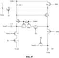
- FIG. 17 is a schematic diagram illustrating the structure of another pixel circuit according to an embodiment of the present application.
- the pixel circuit of the multiple pixel circuits also includes a second voltage writing control transistor T11 connected between a second electrode of the drive transistor T1 and the second electrode of the second leakage compensation transistor T9.
- the second voltage writing control transistor T11 may be a double-gate transistor or a single-gate transistor.
- the second voltage writing control transistor T11 and the first leakage compensation transistor T8 are connected to the same scan signal. Therefore, the pixel circuit is also applicable to the drive timings shown in FIGS. 10 and 11 and also applicable to the drive timings shown in FIGS. 13 and 14 . Additionally, the second voltage writing control transistor T11 and the threshold compensation transistor T5 are connected in series. Thus, at the black frame insertion stage, since the fifth scan signal transmitted on the fifth scan line EM is always a high level, and the second voltage writing control transistor T11, the second leakage compensation transistor T9, and the first leakage compensation transistor T8 are always in the off state, the data voltage is not written into the gate of the drive transistor T1 even if the data writing transistor T2 and the threshold compensation transistor T5 are turned on.
- the second scan signal transmitted on the second scan line S2 may be configured as a high-frequency signal, and the second scan signal, the first scan signal, and the fourth scan signal may be generated by the same set of gate drive circuits, which facilitates a narrow frame design.
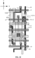
- FIG. 18 is a schematic diagram illustrating the structure of another array substrate according to an embodiment of the present application.
- FIG. 18 shows a layout structure corresponding to the pixel circuit shown in FIG. 17 .
- the structure of the active layer 10 is optimized, and the active layer 10 overlapping the second metal wire 12 extends in the first direction and overlaps the fifth metal wire 15 such that the overlapping portion of the fifth metal wire 15 and the active layer 10 forms the second voltage writing control transistor T11 (including a first sub-transistor T11-1 and a second sub-transistor T11-2), the first leakage compensation transistor T8, and the second leakage compensation transistor T9.
- the space utilization of the layout is improved.
- FIG. 19 is a schematic diagram illustrating the structure of another array substrate according to an embodiment of the present application.
- FIG. 19 shows another layout structure corresponding to the pixel circuit shown in FIG. 17 .
- the first sub-metal wire 111 and the second sub-metal wire 112 are connected together, and since the second sub-metal wire 112 is also connected to the second metal wire 12, the first metal wire 11 and the second metal wire 12 are connected to each other to form a horizontal and vertical mesh structure.
- the threshold compensation effect of the drive transistor T1 may be improved by drive timing (such as double pulse timing as shown in FIG. 13 ).
- the non-uniformity of the drive current is improved to enhance the display effect.
- FIG. 20 is a schematic diagram illustrating the structure of another array substrate according to an embodiment of the present application.
- FIG. 20 shows another layout structure corresponding to the pixel circuit shown in FIG. 17 .
- the third metal wire 13 includes a first body portion 131 and a first branch portion 132.
- the fourth metal wire 14 includes a second body portion 141 and a second branch portion 142.
- the first body portion 131 and the second body portion 141 extend in the second direction.
- the first branch portion 132 and the second branch portion 142 extend in the first direction.
- the active layer 10 forming the second leakage compensation transistor T9 extends upward in the first direction and then extends in the second direction to overlap the first branch portion 132 of the third metal wire 13 to form the first initialization transistor T2.
- the first body portion 131 of the third metal wire 13 overlaps the active layer 10 to form the second initialization transistor T3 of the pixel circuit in the previous row.
- the second body portion 141 of the fourth metal wire 14 overlaps the active layer 10 extending in the first direction to form the second initialization transistor T3 of the pixel circuit in the current row.
- the second branch portion 142 of the fourth metal wire 14 overlaps the active layer 10 extending in the second direction to form the first initialization transistor T2 of the pixel circuit in the next row.
- the second metal wire 12 is connected to the first initialization transistor T2 and the second initialization transistor T3 via the second sub-metal wire 112, and the first sub-metal wire 111 does not need to be provided so that no vertical line exists for separately transmitting the first initialization voltage Vrefl in the layout structure. Therefore, a larger light transmittance can be obtained.
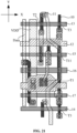
- FIG. 21 is a schematic diagram illustrating the structure of another array substrate according to an embodiment of the present application.
- FIG. 22 is a schematic diagram illustrating the structure of another array substrate according to an embodiment of the present application.
- FIG. 21 and FIG. 22 separately show another layout structure corresponding to the pixel circuit shown in FIG. 17 .
- the second voltage writing control transistor T11 is a single gate transistor.
- the difference is that the first leakage compensation transistor T8 and the second leakage compensation transistor T9 are formed at opposite positions, and the other structures are identical.
- the orthographic projection of the fifth metal wire 15 on the substrate is located between the orthographic projection of the sixth metal wire 16 on the substrate and the orthographic projection of the second metal wire 12 on the substrate so that the distance between the first leakage compensation transistor T8 and the gate of the drive transistor T1 can be made shorter, that is, the leakage path of the gate of the drive transistor T1 is shorter, which helps reduce the coupling effect of other signals on the potential of the gate of the drive transistor T1 and can reduce crosstalk between multiple pixel circuits.
- FIG. 23 is a schematic diagram illustrating the structure of another pixel circuit according to an embodiment of the present application.
- FIG. 24 is a top view illustrating the structure of another array substrate according to an embodiment of the present application.
- FIG. 24 shows a layout structure corresponding to the pixel circuit shown in FIG. 23 .
- the pixel circuit of the multiple pixel circuits may include both a first voltage writing control transistor T10 and a second voltage writing control transistor T11; the first voltage writing control transistor T 10, the second voltage writing control transistor T11, the first leakage compensation transistor T8, and the second leakage compensation transistor T9 are all connected to a fifth metal wire (the third scan line EMB).
- the active layer 10 forming the data writing transistor T4 extends upwardly in the first direction and overlaps the fifth metal wire 15 to form the first voltage writing control transistor T10.
- the active layer 10 forming the data writing transistor T4 extends upwardly in the first direction and overlaps the fifth metal wire 15 to form the first voltage writing control transistor T10.
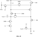
- FIG. 25 is a schematic diagram illustrating the structure of another pixel circuit according to an embodiment of the present application.
- FIG. 26 is a top view illustrating the structure of another array substrate according to an embodiment of the present application.
- FIG. 26 shows a layout structure corresponding to the pixel circuit shown in FIG. 25 .
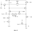
- the threshold compensation transistor T5 may be removed, and the second voltage writing control transistor T11 is reused as the threshold compensation transistor T5, which helps reduce the number of transistors and the space occupied by the layout.
- the orthographic projection of the second metal wire 12 on the substrate is located between the orthographic projection of the fifth metal wire 15 on the substrate and the orthographic projection of the sixth metal wire 16 on the substrate, and the orthographic projection of the fifth metal wire 15 on the substrate is located on a side of the orthographic projection of the second metal wire 12 on the substrate adjacent to the orthographic projection of the gate of the drive transistor T1 on the substrate.
- the distance between the first leakage compensation transistor T8 formed by the overlap of the fifth metal wire 15 and the active layer 10 and the gate of the drive transistor T1 can be further shortened, which helps reduce the coupling effect of other signals on the potential of the gate of the drive transistor T1 and can reduce crosstalk between multiple pixel circuits.
- the first metal wire 11 may also be connected to the second metal wire 12 to form a mesh structure; alternatively, the first metal wire 11 may be removed, and the second metal wire 12 may be used for supplying the initialization voltage to the first initialization transistor T2 and the second initialization transistor T3.
- the specific connection relationship thereof is not described herein again, and reference may be made to the related description in any of the preceding embodiments.
- FIG. 27 is a schematic diagram illustrating the structure of another pixel circuit according to an embodiment of the present application.
- FIG. 28 is a top view illustrating the structure of another array substrate according to an embodiment of the present application.
- FIG. 28 shows a layout structure corresponding to the pixel circuit shown in FIG. 27 .
- the structure of the active layer 10 is changed so that the threshold compensation transistor T5 can be configured as a double-gate transistor to further reduce the leakage current of the gate of the drive transistor T1.
- the sixth metal wire 16 overlaps the active layer 10 to form a threshold compensation transistor T5 (including a third sub-transistor T5-1 and a fourth sub-transistor T5-2) and a data writing transistor T4, respectively.
- FIG. 28 only shows a case in which the first metal wire 11 and the second metal wire 12 are connected together.
- first metal wire 11 and the second metal wire 12 are insulated from each other, reference may be made to the related description in any embodiment described above, and details are not repeated.
- the array substrate provided by this embodiment of the present application in combination with the structure of the pixel circuit, the drive timing, and the layout, can reduce the gate leakage of the drive transistor, help stabilize the drive current, and thus improve the uniformity of display pictures.
- the first metal wire and the second metal wire are configured in layers so that the first metal wire and the second metal wire can transmit different voltages to independently adjust the gate potential of the drive transistor and the anode potential of the light-emitting element. In this manner, the improvement of low-grayscale color cast and low-frequency flickering no longer restrict each other, residual shadows can be improved, and thus the display effect can be greatly enhanced.
- the first metal wire and the second metal wire are in different layers, the first metal wire and the second metal wire can be arranged in a limited space, thereby improving the utilization rate of the layout space.
- an embodiment of the present application also provides a display panel, including the array substrate provided by any embodiment of the present application. Therefore, the display panel also has the beneficial effects described in any of the preceding embodiments.
- FIG. 29 is a view illustrating the structure of a display device according to an embodiment of the present application.
- the display device in this embodiment may be a mobile phone or any electronic product with a display function, including but not limited to a television, a laptop, a desktop display, a tablet computer, a digital camera, a smart bracelet, smart glasses, an in-vehicle display, a medical display, industry-controlling equipment, and a touch interactive terminal.
- This embodiment of the present application is not specifically limited thereto.
Landscapes
- Engineering & Computer Science (AREA)
- Physics & Mathematics (AREA)
- Microelectronics & Electronic Packaging (AREA)
- Computer Hardware Design (AREA)
- General Physics & Mathematics (AREA)
- Theoretical Computer Science (AREA)
- Geometry (AREA)
- Devices For Indicating Variable Information By Combining Individual Elements (AREA)
- Control Of El Displays (AREA)
- Electroluminescent Light Sources (AREA)
- Control Of Indicators Other Than Cathode Ray Tubes (AREA)
Applications Claiming Priority (2)
| Application Number | Priority Date | Filing Date | Title |
|---|---|---|---|
| CN202210751702.8A CN115084165B (zh) | 2022-06-28 | 2022-06-28 | 阵列基板、显示面板和显示装置 |
| PCT/CN2022/115449 WO2024000783A1 (fr) | 2022-06-28 | 2022-08-29 | Substrat matriciel, panneau d'affichage et dispositif d'affichage |
Publications (2)
| Publication Number | Publication Date |
|---|---|
| EP4386845A1 true EP4386845A1 (fr) | 2024-06-19 |
| EP4386845A4 EP4386845A4 (fr) | 2025-09-03 |
Family
ID=83254808
Family Applications (1)
| Application Number | Title | Priority Date | Filing Date |
|---|---|---|---|
| EP22948874.7A Pending EP4386845A4 (fr) | 2022-06-28 | 2022-08-29 | Substrat matriciel, panneau d'affichage et dispositif d'affichage |
Country Status (5)
| Country | Link |
|---|---|
| US (1) | US20240213270A1 (fr) |
| EP (1) | EP4386845A4 (fr) |
| KR (1) | KR102873529B1 (fr) |
| CN (1) | CN115084165B (fr) |
| WO (1) | WO2024000783A1 (fr) |
Families Citing this family (12)
| Publication number | Priority date | Publication date | Assignee | Title |
|---|---|---|---|---|
| KR20240017216A (ko) * | 2022-07-28 | 2024-02-07 | 삼성디스플레이 주식회사 | 화소 회로 및 이를 포함하는 표시 장치 |
| CN116386537B (zh) * | 2022-09-22 | 2026-01-23 | 京东方科技集团股份有限公司 | 一种像素驱动电路及其驱动方法、显示面板 |
| WO2024065614A1 (fr) * | 2022-09-30 | 2024-04-04 | 京东方科技集团股份有限公司 | Circuit d'attaque de pixel, procédé d'attaque et appareil d'affichage associé |
| CN115527487B (zh) * | 2022-10-27 | 2026-01-30 | 昆山国显光电有限公司 | 像素电路及其驱动方法和显示面板 |
| CN115631728B (zh) * | 2022-10-31 | 2025-01-03 | 湖北长江新型显示产业创新中心有限公司 | 一种显示面板及显示装置 |
| CN115938312A (zh) * | 2022-12-15 | 2023-04-07 | 云谷(固安)科技有限公司 | 一种像素电路及显示面板 |
| WO2024197581A1 (fr) * | 2023-03-28 | 2024-10-03 | Boe Technology Group Co., Ltd. | Substrat de réseau et appareil d'affichage |
| CN116403507B (zh) * | 2023-04-11 | 2026-02-27 | 湖北长江新型显示产业创新中心有限公司 | 阵列基板、显示面板及显示装置 |
| CN117037704B (zh) * | 2023-08-31 | 2025-11-21 | 昆山国显光电有限公司 | 像素驱动电路及其驱动方法、显示基板 |
| CN117456954A (zh) * | 2023-11-08 | 2024-01-26 | Tcl华星光电技术有限公司 | 像素驱动电路及显示面板 |
| CN119339669A (zh) * | 2024-12-16 | 2025-01-21 | 惠科股份有限公司 | 驱动电路及其驱动方法、显示面板 |
| CN119495260B (zh) * | 2024-12-20 | 2026-01-27 | 京东方科技集团股份有限公司 | 显示面板及显示装置 |
Family Cites Families (15)
| Publication number | Priority date | Publication date | Assignee | Title |
|---|---|---|---|---|
| CN102832229B (zh) * | 2012-08-31 | 2014-12-10 | 京东方科技集团股份有限公司 | 发光器件的像素电路及驱动方法和显示装置 |
| CN104751804A (zh) * | 2015-04-27 | 2015-07-01 | 京东方科技集团股份有限公司 | 一种像素电路、其驱动方法及相关装置 |
| CN105590955A (zh) * | 2015-12-25 | 2016-05-18 | 昆山国显光电有限公司 | 像素电路及其驱动方法和有源矩阵有机发光显示器 |
| CN106935198B (zh) * | 2017-04-17 | 2019-04-26 | 京东方科技集团股份有限公司 | 一种像素驱动电路、其驱动方法及有机发光显示面板 |
| CN111403465B (zh) * | 2020-03-30 | 2022-10-21 | 昆山国显光电有限公司 | 阵列基板、显示面板和显示装置 |
| KR102891503B1 (ko) * | 2020-04-22 | 2025-11-26 | 삼성디스플레이 주식회사 | 디스플레이 장치 |
| KR102741002B1 (ko) * | 2020-04-29 | 2024-12-12 | 삼성디스플레이 주식회사 | 유기발광 디스플레이 장치 및 그 제조방법 |
| US11751448B2 (en) * | 2020-06-11 | 2023-09-05 | Samsung Display Co., Ltd. | Display device |
| KR102781347B1 (ko) * | 2020-08-05 | 2025-03-12 | 삼성디스플레이 주식회사 | 표시 장치 |
| US11621314B2 (en) * | 2020-09-02 | 2023-04-04 | Samsung Display Co., Ltd. | Display device |
| CN113421514B (zh) * | 2021-06-23 | 2022-09-20 | 昆山国显光电有限公司 | 像素电路及其驱动方法、显示面板及显示装置 |
| CN216488063U (zh) * | 2021-07-30 | 2022-05-10 | 京东方科技集团股份有限公司 | 显示基板及显示装置 |
| CN113823639B (zh) * | 2021-09-09 | 2024-02-27 | 武汉天马微电子有限公司 | 显示面板及显示装置 |
| CN113838424B (zh) * | 2021-09-27 | 2023-04-18 | 武汉华星光电半导体显示技术有限公司 | 一种显示面板 |
| CN114005400B (zh) * | 2021-10-29 | 2024-02-27 | 昆山国显光电有限公司 | 像素电路和显示面板 |
-
2022
- 2022-06-28 CN CN202210751702.8A patent/CN115084165B/zh active Active
- 2022-08-29 EP EP22948874.7A patent/EP4386845A4/fr active Pending
- 2022-08-29 KR KR1020247007466A patent/KR102873529B1/ko active Active
- 2022-08-29 WO PCT/CN2022/115449 patent/WO2024000783A1/fr not_active Ceased
-
2024
- 2024-03-08 US US18/599,753 patent/US20240213270A1/en active Pending
Also Published As
| Publication number | Publication date |
|---|---|
| EP4386845A4 (fr) | 2025-09-03 |
| WO2024000783A1 (fr) | 2024-01-04 |
| KR20240045264A (ko) | 2024-04-05 |
| KR102873529B1 (ko) | 2025-10-21 |
| CN115084165B (zh) | 2023-05-23 |
| US20240213270A1 (en) | 2024-06-27 |
| CN115084165A (zh) | 2022-09-20 |
Similar Documents
| Publication | Publication Date | Title |
|---|---|---|
| EP4386845A1 (fr) | Substrat matriciel, panneau d'affichage et dispositif d'affichage | |
| US11361713B1 (en) | Display panel and display device | |
| CN113013218B (zh) | 阵列基板、显示面板及显示装置 | |
| US11783772B2 (en) | Array substrate, display panel, and display device | |
| US10811438B2 (en) | Thin-film transistor array substrate and organic light-emitting display device including the same | |
| EP3174099B1 (fr) | Affichage à diodes électroluminescentes organiques | |
| EP3929993A1 (fr) | Panneau d'affichage et son procédé d'attaque, et appareil d'affichage | |
| US10657888B2 (en) | Driving method for pixel driving circuit, display panel and display device | |
| JP2021524926A (ja) | 表示パネルおよび表示装置 | |
| CN107481669A (zh) | 一种显示面板及显示装置 | |
| WO2020192208A1 (fr) | Substrat de réseau, panneau d'affichage et appareil d'affichage | |
| KR102771472B1 (ko) | 게이트 드라이버를 갖는 디스플레이 장치 | |
| CN118104419A (zh) | 显示面板及显示装置 | |
| CN113781963A (zh) | 像素电路、显示面板及显示装置 | |
| US11302260B2 (en) | Signal processing circuit and driving method thereof, display panel and driving method thereof and display device | |
| WO2021081703A1 (fr) | Unité de registre à décalage et son procédé de pilotage, circuit de pilotage de grille et dispositif d'affichage | |
| WO2022041227A1 (fr) | Panneau d'affichage et appareil d'affichage | |
| CN117095637A (zh) | 显示设备 | |
| WO2024198172A1 (fr) | Circuit de pixels et panneau d'affichage | |
| CN114203109B (zh) | 像素驱动电路及其补偿方法、显示面板 | |
| CN118471141A (zh) | 一种显示面板及显示装置 | |
| US20250061851A1 (en) | Pixel circuit and driving method thereof, and display device | |
| US12315463B2 (en) | Display panel, driving method for the same, and display apparatus | |
| US20250322792A1 (en) | Pixel driving circuit, display panel and display device | |
| CN114283763B (zh) | 像素驱动电路的布线结构、显示面板和显示装置 |
Legal Events
| Date | Code | Title | Description |
|---|---|---|---|
| STAA | Information on the status of an ep patent application or granted ep patent |
Free format text: STATUS: THE INTERNATIONAL PUBLICATION HAS BEEN MADE |
|
| PUAI | Public reference made under article 153(3) epc to a published international application that has entered the european phase |
Free format text: ORIGINAL CODE: 0009012 |
|
| STAA | Information on the status of an ep patent application or granted ep patent |
Free format text: STATUS: REQUEST FOR EXAMINATION WAS MADE |
|
| 17P | Request for examination filed |
Effective date: 20240312 |
|
| AK | Designated contracting states |
Kind code of ref document: A1 Designated state(s): AL AT BE BG CH CY CZ DE DK EE ES FI FR GB GR HR HU IE IS IT LI LT LU LV MC MK MT NL NO PL PT RO RS SE SI SK SM TR |
|
| REG | Reference to a national code |
Ref country code: DE Ref legal event code: R079 Free format text: PREVIOUS MAIN CLASS: H01L0027120000 Ipc: H10D0086400000 |
|
| A4 | Supplementary search report drawn up and despatched |
Effective date: 20250804 |
|
| RIC1 | Information provided on ipc code assigned before grant |
Ipc: H10D 86/40 20250101AFI20250729BHEP Ipc: G09G 3/3233 20160101ALI20250729BHEP Ipc: H10K 59/131 20230101ALI20250729BHEP Ipc: H10K 59/121 20230101ALI20250729BHEP Ipc: H10D 86/60 20250101ALI20250729BHEP |
|
| DAV | Request for validation of the european patent (deleted) | ||
| DAX | Request for extension of the european patent (deleted) |