EP4386899A1 - Negativelektrodenaktivmaterial und herstellungsverfahren dafür, sekundärbatterie damit und elektrische vorrichtung - Google Patents
Negativelektrodenaktivmaterial und herstellungsverfahren dafür, sekundärbatterie damit und elektrische vorrichtung Download PDFInfo
- Publication number
- EP4386899A1 EP4386899A1 EP22949671.6A EP22949671A EP4386899A1 EP 4386899 A1 EP4386899 A1 EP 4386899A1 EP 22949671 A EP22949671 A EP 22949671A EP 4386899 A1 EP4386899 A1 EP 4386899A1
- Authority
- EP
- European Patent Office
- Prior art keywords
- negative electrode
- silicon
- electrode active
- active material
- based material
- Prior art date
- Legal status (The legal status is an assumption and is not a legal conclusion. Google has not performed a legal analysis and makes no representation as to the accuracy of the status listed.)
- Pending
Links
Images
Classifications
-
- C—CHEMISTRY; METALLURGY
- C01—INORGANIC CHEMISTRY
- C01B—NON-METALLIC ELEMENTS; COMPOUNDS THEREOF; METALLOIDS OR COMPOUNDS THEREOF NOT COVERED BY SUBCLASS C01C
- C01B33/00—Silicon; Compounds thereof
- C01B33/02—Silicon
- C01B33/021—Preparation
-
- H—ELECTRICITY
- H01—ELECTRIC ELEMENTS
- H01M—PROCESSES OR MEANS, e.g. BATTERIES, FOR THE DIRECT CONVERSION OF CHEMICAL ENERGY INTO ELECTRICAL ENERGY
- H01M10/00—Secondary cells; Manufacture thereof
- H01M10/05—Accumulators with non-aqueous electrolyte
- H01M10/052—Li-accumulators
- H01M10/0525—Rocking-chair batteries, i.e. batteries with lithium insertion or intercalation in both electrodes; Lithium-ion batteries
-
- H—ELECTRICITY
- H01—ELECTRIC ELEMENTS
- H01M—PROCESSES OR MEANS, e.g. BATTERIES, FOR THE DIRECT CONVERSION OF CHEMICAL ENERGY INTO ELECTRICAL ENERGY
- H01M4/00—Electrodes
- H01M4/02—Electrodes composed of, or comprising, active material
- H01M4/13—Electrodes for accumulators with non-aqueous electrolyte, e.g. for lithium-accumulators; Processes of manufacture thereof
- H01M4/133—Electrodes based on carbonaceous material, e.g. graphite-intercalation compounds or CFx
-
- H—ELECTRICITY
- H01—ELECTRIC ELEMENTS
- H01M—PROCESSES OR MEANS, e.g. BATTERIES, FOR THE DIRECT CONVERSION OF CHEMICAL ENERGY INTO ELECTRICAL ENERGY
- H01M4/00—Electrodes
- H01M4/02—Electrodes composed of, or comprising, active material
- H01M4/13—Electrodes for accumulators with non-aqueous electrolyte, e.g. for lithium-accumulators; Processes of manufacture thereof
- H01M4/134—Electrodes based on metals, Si or alloys
-
- H—ELECTRICITY
- H01—ELECTRIC ELEMENTS
- H01M—PROCESSES OR MEANS, e.g. BATTERIES, FOR THE DIRECT CONVERSION OF CHEMICAL ENERGY INTO ELECTRICAL ENERGY
- H01M4/00—Electrodes
- H01M4/02—Electrodes composed of, or comprising, active material
- H01M4/36—Selection of substances as active materials, active masses, active liquids
- H01M4/362—Composites
- H01M4/364—Composites as mixtures
-
- H—ELECTRICITY
- H01—ELECTRIC ELEMENTS
- H01M—PROCESSES OR MEANS, e.g. BATTERIES, FOR THE DIRECT CONVERSION OF CHEMICAL ENERGY INTO ELECTRICAL ENERGY
- H01M4/00—Electrodes
- H01M4/02—Electrodes composed of, or comprising, active material
- H01M4/36—Selection of substances as active materials, active masses, active liquids
- H01M4/362—Composites
- H01M4/366—Composites as layered products
-
- H—ELECTRICITY
- H01—ELECTRIC ELEMENTS
- H01M—PROCESSES OR MEANS, e.g. BATTERIES, FOR THE DIRECT CONVERSION OF CHEMICAL ENERGY INTO ELECTRICAL ENERGY
- H01M4/00—Electrodes
- H01M4/02—Electrodes composed of, or comprising, active material
- H01M4/36—Selection of substances as active materials, active masses, active liquids
- H01M4/38—Selection of substances as active materials, active masses, active liquids of elements or alloys
- H01M4/386—Silicon or alloys based on silicon
-
- H—ELECTRICITY
- H01—ELECTRIC ELEMENTS
- H01M—PROCESSES OR MEANS, e.g. BATTERIES, FOR THE DIRECT CONVERSION OF CHEMICAL ENERGY INTO ELECTRICAL ENERGY
- H01M4/00—Electrodes
- H01M4/02—Electrodes composed of, or comprising, active material
- H01M4/36—Selection of substances as active materials, active masses, active liquids
- H01M4/58—Selection of substances as active materials, active masses, active liquids of inorganic compounds other than oxides or hydroxides, e.g. sulfides, selenides, tellurides, halogenides or LiCoFy; of polyanionic structures, e.g. phosphates, silicates or borates
- H01M4/583—Carbonaceous material, e.g. graphite-intercalation compounds or CFx
- H01M4/587—Carbonaceous material, e.g. graphite-intercalation compounds or CFx for inserting or intercalating light metals
-
- H—ELECTRICITY
- H01—ELECTRIC ELEMENTS
- H01M—PROCESSES OR MEANS, e.g. BATTERIES, FOR THE DIRECT CONVERSION OF CHEMICAL ENERGY INTO ELECTRICAL ENERGY
- H01M4/00—Electrodes
- H01M4/02—Electrodes composed of, or comprising, active material
- H01M4/62—Selection of inactive substances as ingredients for active masses, e.g. binders, fillers
- H01M4/624—Electric conductive fillers
- H01M4/625—Carbon or graphite
-
- C—CHEMISTRY; METALLURGY
- C01—INORGANIC CHEMISTRY
- C01P—INDEXING SCHEME RELATING TO STRUCTURAL AND PHYSICAL ASPECTS OF SOLID INORGANIC COMPOUNDS
- C01P2004/00—Particle morphology
- C01P2004/60—Particles characterised by their size
- C01P2004/64—Nanometer sized, i.e. from 1-100 nanometer
-
- C—CHEMISTRY; METALLURGY
- C01—INORGANIC CHEMISTRY
- C01P—INDEXING SCHEME RELATING TO STRUCTURAL AND PHYSICAL ASPECTS OF SOLID INORGANIC COMPOUNDS
- C01P2004/00—Particle morphology
- C01P2004/80—Particles consisting of a mixture of two or more inorganic phases
-
- C—CHEMISTRY; METALLURGY
- C01—INORGANIC CHEMISTRY
- C01P—INDEXING SCHEME RELATING TO STRUCTURAL AND PHYSICAL ASPECTS OF SOLID INORGANIC COMPOUNDS
- C01P2006/00—Physical properties of inorganic compounds
- C01P2006/12—Surface area
-
- C—CHEMISTRY; METALLURGY
- C01—INORGANIC CHEMISTRY
- C01P—INDEXING SCHEME RELATING TO STRUCTURAL AND PHYSICAL ASPECTS OF SOLID INORGANIC COMPOUNDS
- C01P2006/00—Physical properties of inorganic compounds
- C01P2006/14—Pore volume
-
- C—CHEMISTRY; METALLURGY
- C01—INORGANIC CHEMISTRY
- C01P—INDEXING SCHEME RELATING TO STRUCTURAL AND PHYSICAL ASPECTS OF SOLID INORGANIC COMPOUNDS
- C01P2006/00—Physical properties of inorganic compounds
- C01P2006/40—Electric properties
-
- H—ELECTRICITY
- H01—ELECTRIC ELEMENTS
- H01M—PROCESSES OR MEANS, e.g. BATTERIES, FOR THE DIRECT CONVERSION OF CHEMICAL ENERGY INTO ELECTRICAL ENERGY
- H01M4/00—Electrodes
- H01M4/02—Electrodes composed of, or comprising, active material
- H01M2004/021—Physical characteristics, e.g. porosity, surface area
-
- H—ELECTRICITY
- H01—ELECTRIC ELEMENTS
- H01M—PROCESSES OR MEANS, e.g. BATTERIES, FOR THE DIRECT CONVERSION OF CHEMICAL ENERGY INTO ELECTRICAL ENERGY
- H01M4/00—Electrodes
- H01M4/02—Electrodes composed of, or comprising, active material
- H01M2004/026—Electrodes composed of, or comprising, active material characterised by the polarity
- H01M2004/027—Negative electrodes
-
- Y—GENERAL TAGGING OF NEW TECHNOLOGICAL DEVELOPMENTS; GENERAL TAGGING OF CROSS-SECTIONAL TECHNOLOGIES SPANNING OVER SEVERAL SECTIONS OF THE IPC; TECHNICAL SUBJECTS COVERED BY FORMER USPC CROSS-REFERENCE ART COLLECTIONS [XRACs] AND DIGESTS
- Y02—TECHNOLOGIES OR APPLICATIONS FOR MITIGATION OR ADAPTATION AGAINST CLIMATE CHANGE
- Y02E—REDUCTION OF GREENHOUSE GAS [GHG] EMISSIONS, RELATED TO ENERGY GENERATION, TRANSMISSION OR DISTRIBUTION
- Y02E60/00—Enabling technologies; Technologies with a potential or indirect contribution to GHG emissions mitigation
- Y02E60/10—Energy storage using batteries
Definitions
- the present application belongs to the field of battery technology, and in particular relates to a negative electrode active material and a method for preparation thereof, as well as a secondary battery comprising the same and an electrical device.
- An object of the present application is to provide a negative electrode active material and a method for preparation thereof, as well as a secondary battery comprising the same and an electrical device, wherein the negative electrode active material has high capacity, high First Coulombic Efficiency and low volume expansion, and can result in a secondary battery having high energy density, high First Coulombic Efficiency, long cycle life and long storage life at the same time.
- the first aspect of the present application provides a negative electrode active material comprising a matrix material and a silicon-based material, the matrix material comprises a plurality of pore structures, at least a part of the silicon-based material is located in pore structures of the matrix material, the silicon-based material comprises a crystalline silicon-based material, a region formed by extending from outer surface of particle of the negative electrode active material to inside of the particle by a distance of 0.5 times a length between any point on the outer surface of the particle of the negative electrode active material and a core of the particle is recorded as an outer region, and a region inside the outer region is recorded as an inner region, and in cross-sectional image of the negative electrode active material, total cross-sectional area of the crystalline silicon-based material in the outer region is smaller than total cross-sectional area of the crystalline silicon-based material in the inner region.
- the negative electrode active material provided in this application comprises a substrate material having a plurality of pore structures and a silicon-based material at least a part of which is located in the pore structures of the matrix material, the silicon-based material comprises a crystalline silicon-based material, and in cross-sectional image of the negative electrode active material, total cross-sectional area of the crystalline silicon-based material in the outer region is smaller than total cross-sectional area of the crystalline silicon-based material in the inner region.
- the crystalline silicon-based material is mainly located in the inner region of the negative electrode active material, and in turn, the negative electrode active material provided in this application can have high capacity, high First Coulombic Efficiency and low volume expansion, and the resulting secondary battery can have high energy density, high First Coulombic Efficiency, long cycle life and long storage life at the same time.
- the cross-sectional image of the negative electrode active material comprises a cross-sectional image passing through the core of particle of the negative electrode active material.
- a ratio ⁇ 1 of the total cross-sectional area of the crystalline silicon-based material in the outer region to the total cross-sectional area of the crystalline silicon-based material in the inner region is (0-50): 100, optionally (0-10): 100.
- the silicon-based material also comprises an amorphous silicon-based material.
- total cross-sectional area of the amorphous silicon-based material in the outer region is greater than total cross-sectional area of the amorphous silicon-based material in the inner region.
- a ratio ⁇ 2 of the total cross-sectional area of the amorphous silicon-based material in the inner region to the total cross-sectional area of the amorphous silicon-based material in the outer region is (0-30): 100, optionally (0-10): 100.
- the outer region of the negative electrode active material mainly contains the amorphous silicon-based material and does not contain or contains a small amount of the crystalline silicon-based material.
- a ratio ⁇ 1 of the total cross-sectional area of the crystalline silicon-based material to the total cross-sectional area of the amorphous silicon-based material is (0-25): 100, optionally (0-5): 100, and more optionally the total cross-sectional area of the crystalline silicon-based material is 0.
- the outer region of the negative electrode active material mainly contains the amorphous silicon-based material and does not contain or contains a small amount of the crystalline silicon-based material.
- a ratio ⁇ 2 of the total cross-sectional area of the crystalline silicon-based material to the total cross-sectional area of the amorphous silicon-based material is 100:(0-250), optionally 100:(0-100).
- the inner region of the negative electrode active material may only contain the crystalline silicon-based material, or may simultaneously contain a mixture of the crystalline silicon-based material and the amorphous silicon-based material, and by further adjusting the total cross-sectional area of the crystalline silicon-based material and the total cross-sectional area of the amorphous silicon-based material within an appropriate range, the improvement effect of the crystalline silicon-based material on the First Coulombic Efficiency can be better exerted.
- the ratio ⁇ 1 of the total cross-sectional area of the crystalline silicon-based material to the total cross-sectional area of the negative electrode active material is greater than 0 and less than or equal to 25%, and optionally from 5% to 20%.
- the total cross-sectional area of the crystalline silicon-based material is within the above ranges, not only the improvement effect of the crystalline silicon-based material on the First Coulombic Efficiency can be fully exerted, and but also a relatively large adverse effect on the cycle performance and storage performance of the secondary battery can be avoided.
- a ratio ⁇ 2 of the total cross-sectional area of the amorphous silicon-based material to the total cross-sectional area of the negative electrode active material is greater than or equal to 35% and less than 100%, optionally from 40% to 60%.
- the total cross-sectional area of the amorphous silicon-based material is within the above-mentioned ranges, not only the improvement effect of the amorphous silicon-based material on the cycle performance and reduction effect of the volume expansion can be fully exerted, and but also a relatively large adverse effect of the amorphous silicon-based material on the First Coulombic Efficiency of the secondary battery can be avoided.
- mass percentage amount of the crystalline silicon-based material in the silicon-based material is greater than 0 and less than or equal to 40 wt%, optionally from 10 wt% to 30 wt%.
- amount of the crystalline silicon-based material is within the above ranges, not only the improvement effect of the crystalline silicon-based material on the First Coulombic Efficiency can be fully exerted, and but also a relatively large adverse effect of the crystalline silicon-based material on the cycle performance and storage performance of the secondary battery can be avoided.
- At least a part of the silicon-based material is located in the pore structures of the matrix material, and there is/are internal void(s) between the silicon-based material and the matrix material.
- this part of the internal void(s) can serve as a space for accommodating the volume expansion of the silicon-based material, and buffer the stress generated during the expansion process of the silicon-based material.
- the crystalline silicon-based material has a grain size of greater than 0 nm and less than or equal to 10 nm, optionally from 2 nm to 8 nm.
- the crystalline silicon-based material has an appropriate grain size, the First Coulombic Efficiency of the secondary battery can be improved, and at the same time, a relatively large adverse effect on the cycle performance and storage performance of the secondary battery can be avoided
- the crystalline silicon-based material comprises one or more of crystalline elemental silicon, silicon oxide, silicon-carbon material, silicon-nitrogen composite, and silicon alloy, and optionally the crystalline silicon-based material comprises crystalline elemental silicon.
- the amorphous silicon-based material comprises one or more of amorphous elemental silicon, silicon oxide, silicon-carbon material, silicon-nitrogen composite, and silicon alloy, and optionally the amorphous silicon-based material comprises amorphous elemental silicon.
- the silicon-based material comprises a vapor-deposited silicon-based material, optionally comprises vapor-deposited elemental silicon.
- the matrix material has a porosity of from 30% to 60%, optionally from 40% to 50%.
- the porosity of the matrix material is within the above ranges, it is beneficial to accommodating sufficient silicon-based materials, which in turn is beneficial to increasing the energy density of the secondary battery.
- the matrix material comprises one or more of carbon material, graphite material and transition metal oxide material.
- the matrix material comprises a carbon material
- the carbon material comprises one or more of activated carbon, biomass carbon, pyrolytic carbon and resin carbon.
- the negative electrode active material further comprises a coating layer which is located on at least part of surface of the matrix material.
- the coating layer located on the outside of the negative electrode active material it can further prevent a direct contact between the silicon-based material and an electrolyte, and reduce the reactivity of the silicon-based material after contact with air, thereby reducing side reaction of the electrolyte and reducing the consumption of active ions and improving the cycle performance of the secondary battery.
- the coating layer comprises one or more of carbon materials, conductive polymers, metal oxides and metal sulfides.
- the coating layer comprises carbon material, and optionally, the carbon material comprises one or more of hard carbon, soft carbon, graphene, carbon fiber, and carbon nanotube.
- the coating layer comprises carbon material, it further helps to improve the conductivity of the silicon-based material.
- the coating layer has a thickness of from 0 nm to 200 nm, optionally from 10 nm to 150 nm.
- the thickness of the coating layer is within the above ranges, it is beneficial for the negative electrode active material to having high specific capacity and low volume expansion.
- the negative electrode active material comprises carbon element and silicon element.
- mass percentage amount of carbon element in the negative electrode active material is from 40 wt% to 60 wt%, optionally from 45 wt% to 50 wt%. In any embodiment of the present application, mass percentage amount of silicon in the negative electrode active material is from 38 wt% to 58 wt%, optionally from 40 wt% 55 wt%.
- the amount of carbon element and/or the amount of silicon element in the negative electrode active material is within the above range, it is beneficial for the negative electrode active material to having both high specific capacity and high conductivity.
- the negative electrode active material further comprises other element(s) including one or more of oxygen element, metal element and nitrogen element.
- a sum of mass percentage amount(s) of other element(s) in the negative electrode active material is from 0 wt% to 20 wt%, optionally from 0 wt% 10 wt%.
- the negative electrode active material has a pore volume of from 0.001 cm 3 /g to 0.02 cm 3 /g, optionally from 0.01 cm 3 /g to 0.02 cm 3 /g.
- the internal void(s) of the negative electrode active material is/are in an appropriate range, which on the one hand can improve the specific capacity and the First Coulombic Efficiency of the negative electrode active material, and on the other hand can buffer the stress generated during the expansion process of the silicon-based material.
- the negative electrode active material has an average particle size Dv50 of from 4 ⁇ m to 12 ⁇ m.
- the average particle size Dv50 of the negative electrode active material helps to reduce surface activity, reduce interfacial side reactions, reduce the consumption for SEI film formation, and also helps to improve active ion and electron transmission performance, thereby further improving the cycle performance of the secondary battery.
- the negative electrode active material has a BET specific surface area of from 1 m 2 /g to 15 m 2 /g.
- the BET specific surface area of the negative electrode active material is within the above range, it helps to reduce surface activity, reduce interfacial side reactions, reduce the consumption for SEI film formation, and improve the First Coulombic Efficiency and cycle performance of the secondary battery.
- the second aspect of the present application provides a method for preparing a negative electrode active material, comprising the steps of: providing a matrix material comprising a plurality of pore structures; dispersing a silicon-based material into the pore structures of the matrix material to obtain a negative electrode active material, wherein the negative electrode active material comprises a matrix material and a silicon-based material, the matrix material comprises a plurality of pore structures, and at least a part of the silicon-based material is located in pore structures of the matrix material, the silicon-based material comprises a crystalline silicon-based material, a region formed by extending from outer surface of particle of the negative electrode active material to inside of the particle by a distance of 0.5 times a length between any point on the outer surface of the particle of the negative electrode active material and a core of the particle is recorded as an outer region, and a region inside the outer region is recorded as an inner region, and in cross-sectional image of the negative electrode active material, total cross-sectional area of the crystalline silicon-based material in the outer region is smaller
- the matrix material has a porosity of from 30% to 60%, optionally from 40% to 50%.
- the porosity of the matrix material is within the above ranges, it is beneficial to accommodating sufficient silicon-based materials, which in turn is beneficial to increasing the energy density of the secondary battery.
- the matrix material comprises one or more of carbon material, graphite material and transition metal oxide material.
- the matrix material comprises a carbon material
- the carbon material comprises one or more of activated carbon, biomass carbon, pyrolytic carbon and resin carbon.
- the matrix material has an average particle size Dv50 of from 4 ⁇ m to 12 ⁇ m.
- the average particle size Dv50 of the matrix material is within the above range, it is beneficial to proceeding smoothly the deposition process, and it is also beneficial for the negative electrode active material to having a suitable content of silicon element, a suitable specific surface area and/or a suitable pore volume.
- the step of dispersing the silicon-based material into the pore structures of the matrix material comprises the following steps of: placing the matrix material comprising a plurality of pore structures as a substrate in a reaction furnace, and feeding a first mixture gas comprising silicon source gas and depositing at a first temperature T 1 for a first time t 1 , stopping feeding of the first mixture gas at the end of depositing; when the temperature in the furnace drops to the second temperature T 2 , feeding a second mixture gas comprising silicon source gas, and depositing at a second temperature T 2 for a second time t 2 , and after the end of depositing, a negative electrode active material is obtained, wherein the silicon-based material comprises crystalline silicon-based material and amorphous silicon-based material, and in cross-sectional image of the negative electrode active material, total cross-sectional area of the crystalline silicon-based material in the outer region is smaller than total cross-sectional area of the crystalline silicon-based material in the inner region; and total cross-sectional area of the
- the method further comprises the steps of: before feeding the first mixture gas comprising silicon source gas, placing the matrix material comprising a plurality of pore structures as a substrate in the reaction furnace, and purging with a protective gas for purge treatment and pre-heating treatment, optionally, the temperature for pre-heating is from 200°C to 300°C. This facilitates the removal of residual moisture in the matrix material, and further facilitates subsequent smooth deposition and formation of the crystalline silicon-based material.
- a volume percentage V 1 of the silicon source gas in the first mixture gas is greater than a volume percentage V 2 of the silicon source gas in the second mixture gas.
- T 1 >T 2 .
- the first temperature during deposition it is beneficial to adjusting the distribution area of the crystalline silicon-based material and the amorphous silicon-based material so that the crystalline silicon-based material is mainly located in the inner region of the negative electrode active material and the amorphous silicon-based material is mainly located in the outer region of the negative electrode active material.
- the improvement effect of the crystalline silicon-based material on the First Coulombic Efficiency can be fully exerted, but also the improvement effect of the amorphous silicon-based material on cycle performance and the reduction effect of the amorphous silicon-based material on volume expansion can be fully exerted.
- t 1 ⁇ t 2 t 1 ⁇ t 2 .
- the first mixture gas comprises a silicon source gas and a protective gas, and optionally, the volume percentage V 1 of the silicon source gas in the first mixture gas is from 10% to 50%.
- the first mixture gas has a total gas flow rate of from 0.5 L/min to 20 L/min.
- the first temperature T 1 is from 500°C to 700°C. In any embodiment of the present application, the first time t 1 is from 0.5 h to 8 h, optionally from 0.5 h to 4 h.
- the second mixture gas comprises a silicon source gas and a protective gas, and optionally, the volume percentage V 2 of the silicon source gas in the second mixture gas is from 5% to 20%.
- the second mixture gas comprises a silicon source gas, a carbon source gas and a protective gas, and optionally, the volume percentage V 2 of the silicon source gas in the second mixture gas is from 5% to 20%, and the volume percentage of the carbon source gas is from 5% to 10%.
- the second mixture gas has a total gas flow rate of from 0.5 L/min to 20 L/min.
- the second temperature T 2 is from 400°C to 500°C. In any embodiment of the present application, the second time t 2 is from 2 h to 16 h, optionally from 4 h to 16 h.
- the composition of the second mixture gas By adjusting at least one of the composition of the second mixture gas, the total gas flow rate of the second mixture gas, the second temperature, and the second time within the above ranges, it is beneficial to forming the amorphous silicon-based material, and it is also beneficial to adjusting parameters such as distribution area and deposition amount of the amorphous silicon-based material.
- the total gas flow rate of the second mixture gas is the same as that of the first mixture gas.
- the method also comprises the following step of: forming a coating layer on at least part of surface of the obtained negative electrode active material, and the coating layer comprises one or more of carbon materials, conductive polymers, metal oxides and metal sulfides.
- the step of forming a coating layer comprising the following steps of: placing the obtained negative electrode active material in a reaction furnace, feeding the third mixture gas containing carbon source gas, and depositing at a third temperature T 3 for a third time t 3 , to obtain a carbon-coated negative electrode active material. This facilitates the formation of a uniform carbon layer.
- the third mixture gas comprises a carbon source gas and a protective gas, and optionally, the volume percentage V 3 of the carbon source gas in the third mixture gas is from 10% to 50%.
- the third mixture gas has a total gas flow rate of from 0.5 L/min to 20 L/min.
- the third temperature T 3 is from 600°C to 700°C. In any embodiment of the present application, the third time t is from 0.5 h to 2 h.
- the composition of the third mixture gas By adjusting at least one of the composition of the third mixture gas, the total gas flow rate of the third mixture gas, the third temperature, and the third time within the above ranges, it is beneficial to forming a coating layer having a suitable thickness and avoiding a coating layer having an excessive thickness which may reduce the First Coulombic Efficiency and/or specific capacity of the negative electrode active material.
- a third aspect of the present application provides a secondary battery, comprising a negative electrode plate, said negative electrode plate comprises the negative electrode active material of the first aspect of this application or the negative electrode active material prepared by the method of the second aspect of this application.
- a fourth aspect of the present application provides an electrical device, comprising the secondary battery according to the third aspect of the present application.
- the negative electrode active material provided by the present application has high capacity, high First Coulombic Efficiency and low volume expansion, and can further result in a secondary battery having high energy density, high First Coulombic Efficiency, long cycle life and long storage life at the same time.
- the electrical device of the present application comprises the secondary battery provided by the present application, and thus has at least the same advantages as the secondary battery.
- ranges disclosed herein are defined in terms of lower and upper limits, and a given range is defined by selecting a lower limit and an upper limit that define the boundaries of the particular range. Ranges defined in this manner may be inclusive or exclusive of end values and may be combined arbitrarily, that is, any lower limit may be combined with any upper limit to form a range. For example, if ranges of 60-120 and 80-110 are listed for a particular parameter, it is to be understood that ranges of 60-110 and 80-120 are also contemplated. Additionally, if the minimum range values 1 and 2 are listed, and the maximum range values 3, 4, and 5 are listed, the following ranges are all expected: 1-3, 1-4, 1-5, 2-3, 2-4 and 2-5.
- the numerical range "a-b” represents an abbreviated representation of any combination of real numbers between a and b, where both a and b are real numbers.
- the numerical range "0-5" means that all real numbers between "0-5" have been listed herein, and the range "0-5" is just an abbreviated representation of the combination of these numerical values.
- a parameter is expressed as an integer greater than or equal to 2, it is equivalent to disclose that the parameter is, for example, an integer of 2, 3, 4, 5, 6, 7, 8, 9, 10, 11, 12, and the like.
- the method includes steps (a) and (b), indicating that the method may include steps (a) and (b) performed in sequence, or that the method may include steps (b) and (a) performed in sequence.
- step (c) indicates that step (c) may be added to the method in any order.
- the method may comprises steps (a), (b) and (c), steps (a), (c) and (b), or steps (c), (a) and (b), and the like.
- transition phases “comprising” and “including” mentioned in the present application means that it is drafted in an open mode or in a close mode.
- the transition phases “comprising” and “including” may mean that other components not listed may also be included or contained, or only the listed components may be included or contained.
- the term "or” is inclusive.
- the phrase "A or B” means “A, B, or both A and B.” More specifically, any of the following conditions satisfy the condition "A or B”: A is true (or exists) and B is false (or does not exist); A is false (or does not exist) and B is true (or exists); or both A and B are true (or exist).
- a specific region such as an inner region or an outer region
- the corresponding material for example, the crystalline silicon-based material or the amorphous silicon-based material
- the corresponding material for example, the crystalline silicon-based material or the amorphous silicon-based material
- silicon has a theoretical specific capacity of up to 4200 mAh/g, which can significantly increase the energy density of secondary batteries; silicon further has a voltage platform slightly higher than graphite, so the negative electrode is not easy to form dendrites, which can improve the safety performance of secondary batteries; silicon is widely distributed in the earth's crust, rich in resources, and low in price, which can reduce the production cost of secondary batteries. Therefore, materials containing silicon (hereinafter referred to as silicon-based materials) have become extremely potential negative electrode active materials.
- silicon is a semiconductor material with low intrinsic conductivity. When used as a negative electrode active material, it will affect the capacity exertion of the secondary battery, or it requires an additionally increased amount of conductive agent, which will reduce actual coating weight of the negative electrode active material and affect the energy density of secondary batteries.
- the main modification methods for the purpose of solving the above problems include the following aspects.
- the inventors of the present application propose a new type of negative electrode active material which has high capacity, high First Coulombic Efficiency and low volume expansion, and can result in a secondary battery better having high energy density, high First Coulombic Efficiency, long cycle life and long storage life at the same time.
- the first aspect of embodiments of the present application provides a negative electrode active material.
- the negative electrode active material comprises a matrix material and a silicon-based material, the matrix material comprises a plurality of pore structures, at least a part of the silicon-based material is located in pore structures of the matrix material, the silicon-based material comprises a crystalline silicon-based material, a region formed by extending from outer surface of particle of the negative electrode active material to inside of the particle by a distance of 0.5 times a length between any point on the outer surface of the particle of the negative electrode active material and a core of the particle is recorded as an outer region, and a region inside the outer region is recorded as an inner region, and in cross-sectional image of the negative electrode active material, total cross-sectional area of the crystalline silicon-based material in the outer region is smaller than total cross-sectional area of the crystalline silicon-based material in the inner region.
- dual beam focused ion beam microscope may be used to prepare a cross-section of the negative electrode active material particle, which cross section passes through the central region of the negative electrode active material, optionally through the particle core of the negative electrode active material, and then the cross-sectional image characteristics of the negative electrode active material can be observed by using a Transmission Electron Microscope (TEM for short) or a High Resolution Transmission Electron Microscope (HRTEM for short).
- TEM Transmission Electron Microscope
- HRTEM High Resolution Transmission Electron Microscope
- particle core or “core of particle” refers to the intersection point of the longest diameter (or longest diagonal) and shortest diameter (or shortest diagonal) of particle of the negative electrode active material.
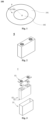
- Fig. 1 is a schematic diagram of a cross-sectional image of an embodiment of a negative electrode active material 100 of the present application and the cross-sectional image passes through the core of particle of the negative electrode active material.
- the negative electrode active material 100 comprises an outer region 101 and an inner region 102 located inside the outer region 101, the intersection point of the longest diameter (or longest diagonal) and the shortest diameter (or shortest diagonal) of the negative electrode active material particle is the particle core O, and the length between any point P on the outer surface of the particle and the particle core O is recorded as R n , and the region formed by extending from the outer surface of the particle of the negative electrode active material to inside of the particle by the distance of 0.5 times the length R n between any point P on the outer surface of the particle and the core O of the particle is recorded as the outer region 101.
- the “length R n” refers to the length from any point on the outer surface of the particle to the core of particle.
- the length R n is expressed as a variable value, that is, the distance from different positions on the outer surface of the particle to the core of particle is a constantly changing value, so the distance extending from different positions on the outer surface of the particle to the inside of the particle is also a constantly changing value. Therefore, after all points on the outer surface of the negative electrode active material particle extend a corresponding distance to the inside of the particle (that is, 0.5 R n ), the region enclosed by all the points and the outer surface of the particle is the outer region.
- total cross-sectional area of the crystalline silicon-based material in the outer region is smaller than total cross-sectional area of the crystalline silicon-based material in the inner region
- the outer region must contain the crystalline silicon-based material; when the outer region does not contain the crystalline silicon-based material, i.e. the corresponding total cross-sectional area of the crystalline silicon-based material in the outer region is 0, it is also considered that the requirement "total cross-sectional area of the crystalline silicon-based material in the outer region is smaller than total cross-sectional area of the crystalline silicon-based material in the inner region" is met.
- the negative electrode active material provided in this application comprises a substrate material having a plurality of pore structures and a silicon-based material at least a part of which is located in the pore structures of the matrix material, the silicon-based material comprises a crystalline silicon-based material, and in cross-sectional image of the negative electrode active material, total cross-sectional area of the crystalline silicon-based material in the outer region is smaller than total cross-sectional area of the crystalline silicon-based material in the inner region.
- the crystalline silicon-based material helps improve the first Coulombic efficiency of secondary batteries.
- the crystalline silicon-based material has large volume expansion and poor structural stability, which is not conducive to improving the cycling performance of secondary batteries and reducing the volume expansion of secondary batteries.
- the crystalline silicon-based material mainly located in the inner region of the negative electrode active material, not only the improvement effect of the crystalline silicon-based material on the First Coulombic Efficiency can be fully exerted, but also a relatively large adverse effect of the crystalline silicon-based material on the cycle performance and storage performance of the secondary battery can be avoided.
- the negative electrode active material provided in this application can have high capacity, high First Coulombic Efficiency and low volume expansion, and the resulting secondary battery can have high energy density, high First Coulombic Efficiency, long cycle life and long storage life at the same time.
- the silicon-based material also comprises an amorphous silicon-based material.
- the silicon-based material comprises crystalline silicon-based material and amorphous silicon-based material, and in cross-sectional image of the negative electrode active material, total cross-sectional area of the crystalline silicon-based material in the outer region is smaller than total cross-sectional area of the crystalline silicon-based material in the inner region; and total cross-sectional area of the amorphous silicon-based material in the outer region is larger than total cross-sectional area of the amorphous silicon-based material in the inner region.
- total cross-sectional area of the amorphous silicon-based material in the inner region is larger than total cross-sectional area of the amorphous silicon-based material in the outer region
- total cross-sectional area of the amorphous silicon-based material in the outer region is not limited to the case that the inner region must contain the amorphous silicon-based material; when the inner region does not contain the amorphous silicon-based material, i.e. the corresponding total cross-sectional area of the amorphous silicon-based material in the inner region is 0, it is also considered that the requirement "total cross-sectional area of the amorphous silicon-based material in the inner region is smaller than total cross-sectional area of the amorphous silicon-based material in the outer region" is met.
- the silicon-based material of this application comprises both crystalline silicon-based material and amorphous silicon-based material, and the crystalline silicon-based material is mainly located in the inner region of the negative electrode active material, while the amorphous silicon-based material is mainly located in the outer region of the negative electrode active material.
- the negative electrode active material provided in this application can have high capacity, high First Coulombic Efficiency, and low volume expansion, and can enable the secondary battery to have high energy density, high First Coulombic Efficiency, long cycle life, and long storage life at the same time.
- the crystalline silicon-based material helps improve the first Coulombic efficiency of secondary batteries.
- the crystalline silicon-based material has large volume expansion and poor structural stability, which is not conducive to improving the cycling performance of secondary batteries and reducing the volume expansion of secondary batteries.
- the amorphous silicon-based material has small volume expansion, which is beneficial for improving the cycling performance of secondary batteries and reducing the volume expansion of secondary batteries.
- the amorphous silicon-based material has low First Coulombic Efficiency, resulting in a large loss of actual capacity of secondary batteries.
- the negative electrode active material can have high capacity, high First Coulombic Efficiency, and low volume expansion, and can enable the secondary battery to have high energy density, high First Coulombic Efficiency, long cycle life, and long storage life at the same time.
- a ratio ⁇ 1 of the total cross-sectional area of the crystalline silicon-based material in the outer region to the total cross-sectional area of the crystalline silicon-based material in the inner region is (0-50): 100, optionally (0-40): 100, (0-30): 100, (0-20): 100, (0-15): 100, (0-10): 100, and (0-5): 100.
- the ratio ⁇ 1 of the total cross-sectional area of the crystalline silicon-based material in the outer region to the total cross-sectional area of the crystalline silicon-based material in the inner region may be 0, that is, the above-mentioned outer region of the negative electrode active material does not contain the crystalline silicon-based material.
- the crystalline silicon-based material mainly located in the inner region of the negative electrode active material, not only the improvement effect of the crystalline silicon-based material on the First Coulombic Efficiency can be fully exerted, and but also a relatively large adverse effect of the crystalline silicon-based material on the cycle performance and storage performance of the secondary battery can be avoided.
- a ratio ⁇ 2 of the total cross-sectional area of the amorphous silicon-based material in the inner region to the total cross-sectional area of the amorphous silicon-based material in the outer region is (0-30): 100, optionally (0-25): 100, (0-20): 100, (0-15): 100, (0-10): 100, and (0-5): 100.
- a ratio ⁇ 2 of the total cross-sectional area of the amorphous silicon-based material in the inner region to the total cross-sectional area of the amorphous silicon-based material in the outer region may be 0, that is, the above-mentioned inner region of the negative electrode active material does not contain the amorphous silicon-based material.
- the effect of the amorphous silicon-based material on improving the cycle performance and reducing the volume expansion can be fully exerted.
- a ratio ⁇ 1 of the total cross-sectional area of the crystalline silicon-based material to the total cross-sectional area of the amorphous silicon-based material is (0-25): 100, optionally (0-20): 100, (0-15): 100, (0-10): 100, (0-5): 100, and more optionally the total cross-sectional area of the crystalline silicon-based material is 0, that is, the above-mentioned outer region of the negative electrode active material does not contain the crystalline silicon-based material.
- the outer region of the negative electrode active material mainly contains the amorphous silicon-based material and does not contain or contains a small amount of the crystalline silicon-based material.
- a ratio ⁇ 2 of the total cross-sectional area of the crystalline silicon-based material to the total cross-sectional area of the amorphous silicon-based material is 100:(0-250), optionally 100:(0-100), 100:(0-80), 100:(0-60), 100:(0-40), 100:(0-30), 100:(0-20), 100:(0-10), 100:(0-5).
- the inner region of the negative electrode active material may only contain the crystalline silicon-based material, or may simultaneously contain a mixture of the crystalline silicon-based material and the amorphous silicon-based material, and by further adjusting the total cross-sectional area of the crystalline silicon-based material and the total cross-sectional area of the amorphous silicon-based material within an appropriate range, the improvement effect of the crystalline silicon-based material on the First Coulombic Efficiency can be better exerted.
- the ratio ⁇ 1 of the total cross-sectional area of the crystalline silicon-based material to the total cross-sectional area of the negative electrode active material is greater than 0 and less than or equal to 25%, for example, it may be 5%, 6%, 7%, 8%, 9%, 10%, 11%, 12%, 13%, 14%, 15%, 16%, 17 %, 18%, 19%, 20%, 21%, 22%, 23%, 24%, 25% or in the ranges formed from any of the above values.
- the ratio ⁇ 1 of the total cross-sectional area of the crystalline silicon-based material to the total cross-sectional area of the negative electrode active material is from 5% to 20%, from 8% to 20%, from 10% to 20%, from 12% to 20%, and from 12% to 18%.
- the total cross-sectional area of the crystalline silicon-based material is within the above ranges, not only the improvement effect of the crystalline silicon-based material on the First Coulombic Efficiency can be fully exerted, and but also a relatively large adverse effect on the cycle performance and storage performance of the secondary battery can be avoided.
- a ratio ⁇ 2 of the total cross-sectional area of the amorphous silicon-based material to the total cross-sectional area of the negative electrode active material is greater than or equal to 35% and less than 100%, optionally from 40% to 65%, from 40% to 60%, from 40% to 55%, or from 40% to 50%.
- the total cross-sectional area of the amorphous silicon-based material is within the above-mentioned ranges, not only the improvement effect of the amorphous silicon-based material on the cycle performance and reduction effect of the volume expansion can be fully exerted, and but also a relatively large adverse effect of the amorphous silicon-based material on the First Coulombic Efficiency of the secondary battery can be avoided.
- the mass percentage amount of the crystalline silicon-based material in the silicon-based material is greater than 0 wt% and less than or equal to 40 wt%, for example, it may be in the range of 5 wt%, 10 wt%, 15 wt%, 20 wt%, 25 wt%, 30 wt%, 35 wt%, 40 wt% or in the ranges formed from any of the above values.
- the mass percentage amount of the crystalline silicon-based material in the silicon-based material is from 5 wt% to 40wt%, from 5 wt% to 35 wt%, from 10 wt% to 35 wt%, or from 10 wt% to 30wt%.
- the amount of the crystalline silicon-based material is within the above ranges, not only the improvement effect of the crystalline silicon-based material on the First Coulombic Efficiency can be fully exerted, and but also a relatively large adverse effect of the crystalline silicon-based material on the cycle performance and storage performance of the secondary battery can be avoided.
- At least a part of the silicon-based material is located in the pore structures of the matrix material, and there is/are internal void(s) between the silicon-based material and the matrix material.
- this part of the internal void(s) can serve as a space for accommodating the volume expansion of the silicon-based material, and buffer the stress generated during the expansion process of the silicon-based material.
- the crystalline silicon-based material has a grain size of greater than 0 nm and less than or equal to 10 nm, for example, it may be in the range of 2 nm, 3 nm, 4 nm, 5 nm, 6 nm, 7 nm, 8 nm, 9 nm, 10 nm or in the ranges formed from any of the above values.
- the grain size of the crystalline silicon-based material is from 2 nm to 10 nm or from 2 nm to 8 nm.
- the crystalline silicon-based material has relatively large grain size, it is beneficial to improving the First Coulombic Efficiency of secondary batteries, but it is unfavorable for the cycling performance and storage performance of secondary batteries. Therefore, when the crystalline silicon-based material has an appropriate grain size, the First Coulombic Efficiency of the secondary battery can be improved, and at the same time, a relatively large adverse effect on the cycle performance and storage performance of the secondary battery can be avoided.
- the grain size of the crystalline silicon-based material has meanings well-known in the art, and can be measured with instruments and methods well-known in the art. For example, a High Resolution Transmission Electron Microscope test may be used.
- the crystalline silicon-based material comprises one or more of crystalline elemental silicon, silicon oxide, silicon-carbon material, silicon-nitrogen composite, and silicon alloy, and optionally the crystalline silicon-based material comprises crystalline elemental silicon (also known as crystalline silicon).
- the amorphous silicon-based material comprises one or more of amorphous elemental silicon, silicon oxide, silicon-carbon material, silicon-nitrogen composite, and silicon alloy, and optionally the amorphous silicon-based material comprises amorphous elemental silicon (also known as non-crystalline silicon or amorphous silicon).
- the silicon-based material comprises a vapor-deposited silicon-based material, optionally comprises vapor-deposited elemental silicon.
- the vapor-deposited elemental silicon comprises vapor-deposited crystalline silicon and vapor-deposited amorphous silicon.
- the matrix material includes a plurality of pore structures, and at least a part of the silicon-based material is located in the pore structures of the matrix material. As a result, the matrix material can effectively relieve the volume expansion of the silicon-based material and prevent the silicon-based material or negative electrode active material from breakage and pulverization.
- the matrix material has a porosity of from 30% to 60%, for example, it may be 30%, 35%, 40%, 45%, 50%, 55%, 60% or in the ranges formed from any of the above values.
- the porosity of the matrix material is from 40% to 50%.
- the porosity of the matrix material is within the above ranges, it is beneficial to accommodating sufficient silicon-based materials, which in turn is beneficial to increasing the energy density of the secondary battery.
- the matrix material comprises one or more of carbon material, graphite material and transition metal oxide material. These matrix materials all include a plurality of pore structures, which can relieve the volume expansion of the silicon-based material and can also improve the conductivity of the silicon-based material.
- the matrix material comprises transition metal oxide material.
- the pore structures of the transition metal oxide material are controllable and adjustable, and the pore size is more uniform, which is conducive to the uniform dispersion of silicon-based material.
- the molecular formula of the transition metal oxide is M x O y , 0 ⁇ x ⁇ 2, 0 ⁇ y ⁇ 3, M comprises one or more elements selected from Ni, Co, Mn, Ti and Cu.
- the transition metal oxide comprises one or more of NiO, Ni 2 O 3 , CoO, Co 2 O 3 , MnO, Mn 2 O 3 , TiO, TiO 2 , Ti 2 O 3 , Cu, Cu 2 O and CuO.
- the matrix material comprises graphite material, such as natural graphite.
- graphite material such as natural graphite.
- the matrix material comprises a carbon material
- the carbon material comprises one or more of activated carbon, biomass carbon, pyrolytic carbon and resin carbon.
- the negative electrode active material further comprises a coating layer which is located on at least part of surface of the matrix material.
- the coating layer located on the outside of the negative electrode active material, it can further prevent a direct contact between the silicon-based material and an electrolyte, and reduce the reactivity of the silicon-based material after contact with air, thereby reducing side reaction of the electrolyte and reducing the consumption of active ions and improving the cycle performance of the secondary battery.
- the coating layer can also provide an effect of buffering the volume expansion of the silicon-based material, which further improves the storage performance of the secondary battery.
- the coating layer comprises one or more of carbon materials, conductive polymers, metal oxides and metal sulfides.
- the carbon material comprises one or more of hard carbon, soft carbon, graphene, carbon fiber, and carbon nanotube.
- the conductive polymer comprises one or more of polyaniline, polypyrrole, and polythiophene.
- the metal oxide comprises one or more of iron oxide, zinc oxide, tin oxide, copper oxide and titanium oxide.
- the metal sulfide comprises one or more of tin sulfide, molybdenum sulfide, titanium sulfide, iron sulfide and copper sulfide.
- the coating layer comprises carbon material, and optionally, the carbon material comprises one or more of hard carbon, soft carbon, graphene, carbon fiber, and carbon nanotube. Therefore, in addition to preventing the silicon-based material from being in direct contact with the electrolyte and buffering the volume expansion of the silicon-based material, the coating layer may also contribute part of the capacity to increase the specific capacity of the negative electrode active material. Additionally, when the coating layer comprises carbon material, it further helps to improve the conductivity of the silicon-based material.
- the coating layer has a thickness of from 0 nm to 200 nm, optionally from 10 nm to 200 nm, from 10 nm to 180 nm, and from 10 nm to 150 nm.
- the thickness of the coating layer is within the above ranges, it is beneficial for the negative electrode active material to having high specific capacity and low volume expansion.
- the thickness of the coating layer is 0 nm, it means that the negative electrode active material does not have a coating layer.
- the negative electrode active material comprises carbon element and silicon element.
- the mass percentage amount of carbon element in the negative electrode active material is from 40 wt% to 60 wt%, such as 40 wt%, 42 wt%, 44 wt%, 46 wt%, 48 wt%, 50 wt%, 52 wt%, 54 wt%, 56 wt%, 58 wt%, 60 wt% or in the ranges formed from any of the above values.
- the mass percentage amount of carbon element in the negative electrode active material is from 45 wt% to 50 wt%.
- the mass percentage amount of silicon element in the silicon-based material is from 38 wt% to 58 wt%, such as 40 wt%, 42 wt%, 44 wt%, 46 wt%, 48 wt%, 50 wt%, 52 wt%, 54 wt%, 56 wt%, 58 wt% or in the ranges formed from any of the above values.
- the mass percentage amount of silicon element in the negative electrode active material is from 40 wt% to 55 wt%.
- the amount of carbon element and/or the amount of silicon element in the negative electrode active material is within the above range, it is beneficial for the negative electrode active material to having both high specific capacity and high conductivity.
- the amount of carbon element in the negative electrode active material may be tested with reference to GB/T 20123-2006/ISO 15350:2000, and the test instrument may be an HCS-140 infrared carbon-sulfur analyzer.
- the amount of silicon element in the negative electrode active material may be tested with reference to GB/T 20975.5-2020.
- the negative electrode active material further comprises other element(s) besides carbon and silicon, and the other elements comprises one or more of oxygen element, metal element and nitrogen element.
- the distribution area of the other element(s) is not specifically limited, for example, it may be located in at least one of the coating layer, the silicon-based material and the matrix material.
- a sum of mass percentage amount(s) of other element(s) in the negative electrode active material is from 0 wt% to 20 wt%, optionally from 0 wt% 10 wt% and from 0 wt% 5 wt%.
- the sum of mass percentage amount(s) of other element(s) in the negative electrode active material is 0 wt%, it means that the negative electrode active material does not comprise other elements except carbon and silicon.
- the negative electrode active material has a pore volume of from 0.001 cm 3 /g to 0.02 cm 3 /g, optionally from 0.01 cm 3 /g to 0.02 cm 3 /g.
- the internal void(s) of the negative electrode active material is/are in an appropriate range, which on the one hand can improve the specific capacity and the First Coulombic Efficiency of the negative electrode active material, and on the other hand can buffer the stress generated during the expansion process of the silicon-based material.
- the pore volume of the negative electrode active material has well-known meaning in the art, and may be measured with well-known instruments and methods in the art. For example, it may be tested with reference to GB/T 21650.2-2008.
- the testing instrument may be a TRISTAR II 3020 specific surface area and porosity analyzer from Micromeritics, USA.
- the negative electrode active material has an average particle size Dv50 of from 4 ⁇ m to 12 ⁇ m.
- the average particle size Dv50 of the negative electrode active material helps to reduce surface activity, reduce interfacial side reactions, reduce the consumption for SEI film formation, and also helps to improve active ion and electron transmission performance, thereby further improving the cycle performance of the secondary battery.
- the average particle size Dv50 of the negative electrode active material has well-known meaning in the art, means the corresponding particle size when the cumulative volume distribution percentage of the material reaches 50%, and may be measured with well-known instruments and methods in the art. For example, it may be conveniently measured by using a laser particle size analyzer with reference to GB/T 19077-2016.
- the testing instrument may be a Mastersizer 3000 laser particle size analyzer from Malvern Instruments Co., Ltd., UK.
- the negative electrode active material has a BET specific surface area of from 1 m 2 /g to 15 m 2 /g.
- the BET specific surface area of the negative electrode active material is within the above range, it helps to reduce surface activity, reduce interfacial side reactions, reduce the consumption for SEI film formation, and improve the First Coulombic Efficiency and cycle performance of the secondary battery.
- the BET specific surface area of the negative electrode active material has well-known meaning in the art, and may be measured with well-known instruments and methods in the art.
- a test method with analysis of specific surface area by nitrogen adsorption may be used for testing, referring to GB/T 19587-2017, and the specific surface area can be calculated by the BET (Brunauer Emmett Teller) method, wherein the test method with analysis of specific surface area by nitrogen adsorption may be carried out by using the TRISTAR II 3020 type specific surface area and porosity analyzer from Micromeritics in the United States.
- a second aspect of the present application provides a method for preparation of a negative electrode active material, which is capable of preparing the negative electrode active material of the first aspect of the embodiments of the present application.
- the method comprises the steps of: providing a matrix material comprising a plurality of pore structures; dispersing a silicon-based material into the pore structures of the matrix material to obtain a negative electrode active material, wherein the negative electrode active material comprises a matrix material and a silicon-based material, the matrix material comprises a plurality of pore structures, and at least a part of the silicon-based material is located in pore structures of the matrix material, the silicon-based material comprises a crystalline silicon-based material, a region formed by extending from outer surface of particle of the negative electrode active material to inside of the particle by a distance of 0.5 times a length between any point on the outer surface of the particle of the negative electrode active material and a core of the particle is recorded as an outer region, and a region inside the outer region is recorded as an inner region, and in cross-sectional image of the negative electrode active material, total cross-sectional area of the crystalline silicon-based material in the outer region is smaller than total cross-sectional area of the crystalline silicon-based material in the inner region.
- the matrix material has a porosity of from 30% to 60%, optionally from 40% to 50%.
- porosity of the matrix material is within the above ranges, it is beneficial to proceeding smoothly the deposition process, and it is also beneficial for the negative electrode active material to having a suitable content of silicon element, a suitable specific surface area and/or a suitable pore volume.
- the matrix material has an average particle size Dv50 of from 4 ⁇ m to 12 ⁇ m.
- the average particle size Dv50 of the matrix material is within the above range, it is beneficial to proceeding smoothly the deposition process, and it is also beneficial for the negative electrode active material to having a suitable content of silicon element, a suitable specific surface area and/or a suitable pore volume.
- the silicon-based material has a poor deposition effect, which is not conducive to the subsequent two-stage deposition; when the average particle size Dv50 of the matrix material is too high, it would easily lead to a problem of insufficient deposition of silicon-based materials and thus an excessive specific surface area of the negative electrode active material, which will increase interfacial side reactions, increase irreversible consumption of active ions, and reduce the First Coulombic Efficiency of the negative electrode active material.
- the matrix material comprises one or more of carbon material, graphite material and transition metal oxide material.
- the matrix material comprises a carbon material
- the carbon material comprises one or more of activated carbon, biomass carbon, pyrolytic carbon and resin carbon.
- the matrix material is commercially available, or prepared according to methods known in the art, for example, it may be obtained by high-temperature pyrolysis of organic carbon sources or chemical activation treatment.
- the organic carbon source may comprise one or more of biomass materials and polymer materials.
- the chemical activation treatment can be carried out by using a pore-forming agent (such as an alkaline solution) to create pores on a matrix material (such as a carbon material).
- the step of dispersing the silicon-based material into the pore structures of the matrix material comprises the following steps of: placing the matrix material comprising a plurality of pore structures as a substrate in a reaction furnace, and feeding a first mixture gas comprising silicon source gas and depositing at a first temperature T 1 for a first time t 1 , stopping feeding of the first mixture gas at the end of depositing; when the temperature in the furnace drops to the second temperature T 2 , feeding a second mixture gas comprising silicon source gas, and depositing at a second temperature T 2 for a second time t 2 , and after the end of depositing, a negative electrode active material is obtained, wherein the silicon-based material comprises crystalline silicon-based material and amorphous silicon-based material, and in cross-sectional image of the negative electrode active material, total cross-sectional area of the crystalline silicon-based material in the outer region is smaller than total cross-sectional area of the crystalline silicon-based material in the inner region; and total cross-sectional area of the amorph
- the process for dispersing the silicon-based material into the pore structures of the matrix material is a vapor deposition process, wherein the vapor deposition process comprises a chemical vapor deposition process and/or a physical vapor deposition process, optionally a chemical vapor deposition process, for example, being any one of thermal chemical vapor deposition process, plasma enhanced chemical vapor deposition process, and microwave plasma assisted chemical vapor deposition process.
- the reaction furnace includes, but is not limited to, any one of a deposition furnace, a rotary furnace, a tube furnace, and a fluidized bed.
- This application uses a two-stage vapor deposition process to deposit the crystalline silicon-based material and the amorphous silicon-based material in the pore structures of the matrix material.
- the vapor-phase deposition process is beneficial to better deposition and uniform dispersion of the silicon-based material in the pore structures of the matrix material, and can avoid the problem of agglomeration and/or large amounts of deposition of silicon-based materials on the surface of the matrix material.
- the method further comprises the steps of: before feeding the first mixture gas comprising silicon source gas, placing the matrix material comprising a plurality of pore structures as a substrate some reaction furnace, and purging with a protective gas for purge treatment and pre-heating treatment, optionally, the temperature for pre-heating is from 200°C to 300°C. This facilitates the removal of residual moisture in the matrix material, and further facilitates subsequent smooth deposition and formation of the crystalline silicon-based material.
- a volume percentage V 1 of the silicon source gas in the first mixture gas is greater than a volume percentage V 2 of the silicon source gas in the second mixture gas.
- this helps to adjust the distribution area of the crystalline silicon-based material and the amorphous silicon-based material so that the crystalline silicon-based material is mainly located in the inner region of the negative electrode active material and the amorphous silicon-based material is mainly located in the outer region of the negative electrode active material.
- the improvement effect of the crystalline silicon-based material on the First Coulombic Efficiency can be fully exerted, but also the improvement effect of the amorphous silicon-based material on cycle performance and the reduction effect of the amorphous silicon-based material on volume expansion can be fully exerted.
- T 1 >T 2 .
- t 1 ⁇ t 2 in the step of dispersing the silicon-based material into the pore structures of the matrix material, t 1 ⁇ t 2 .
- the first temperature during deposition to be greater than the second temperature
- the pressure in the furnace can be adjusted to a slight positive pressure after feeding the first mixture gas containing silicon source gas, for example, it may be 200 Pa-600 Pa higher than the atmospheric pressure, thereby facilitating the smooth progress of deposition.
- the first mixture gas comprises a silicon source gas and a protective gas
- the volume percentage V 1 of the silicon source gas in the first mixture gas is from 10% to 50%, for example, it may be 10%, 15%, 20%, 25%, 30%, 35%, 40%, 45%, 50% or in the ranges formed from any of the above values.
- the first mixture gas has a total gas flow rate of from 0.5 L/min to 20 L/min.
- it may be 1 L/min, 2 L/min, 3 L/min, 4 L/min, 5 L/min, 6 L/min, 7 L/min, 8 L/min, 9 L/min, 10 L/min, 12 L/min, 14 L/min, 16 L/min, 18 L/min, 20 L/min or in the ranges formed from any of the above values.
- the first temperature T 1 is from 500°C to 700°C, for example, it may be 520°C, 540°C, 560°C, 580°C, 600°C, 620°C, 640°C, 660°C, 680°C, 700°C or in the ranges formed from any of the above values.
- the first time t 1 is from 0.5 h to 8 h, for example, it may be 1 h, 2 h, 3 h, 4 h, 5 h, 6 h, 7 h, 8 h or in the ranges formed from any of the above values.
- the first time t 1 is from 0.5 h to 4 h.
- the composition of the first mixture gas By adjusting at least one of the composition of the first mixture gas, the total gas flow rate of the first mixture gas, the first temperature, and the first time within the above ranges, it is beneficial to forming the crystalline silicon-based material, and it is also beneficial to adjusting parameters such as distribution area, and grain size and deposition amount of the crystalline silicon-based material.
- the volume percentage of the silicon source gas in the first mixture gas is too high and/or the total gas flow rate of the first mixture gas is too high, the amount and distribution area of the crystalline silicon-based material increase, thereby adversely affecting the improvement of cycle performance and storage performance of the secondary battery.
- the volume percentage of the silicon source gas in the first mixture gas is too low and/or the total gas flow rate of the first mixture gas is too low, the deposition amount of the crystalline silicon-based material may be insufficient, thereby adversely affecting the improvement of the First Coulombic Efficiency of the secondary battery.
- the first temperature is too low, it is not conducive to the formation of the crystalline silicon-based material.
- the grain size of the silicon-based material increases, thereby adversely affecting the improvement of the improvement of the cycle performance and storage performance of the secondary battery.
- the deposition amount of the crystalline silicon-based material may be insufficient, thereby adversely affecting the improvement of the First Coulombic Efficiency of the secondary battery.
- the amount and distribution area of the crystalline silicon-based material increase, thereby adversely affecting the improvement of the cycle performance and storage performance of the secondary battery.
- the pressure in the furnace can be adjusted to a slight positive pressure after feeding the second mixture gas containing silicon source gas, for example, it may be 200 Pa-600 Pa higher than the atmospheric pressure, thereby facilitating the smooth progress of deposition.
- the second mixture gas comprises a silicon source gas and a protective gas, and optionally, the volume percentage V 2 of the silicon source gas in the second mixture gas is from 5% to 20%, for example, it may be 5%, 6%, 8%, 10%, 12%, 14%, 16%, 18%, 20%, or in the ranges formed from any of the above values.
- the second mixture gas may comprise a silicon source gas, a carbon source gas and a protective gas, and optionally, the volume percentage V 2 of the silicon source gas in the second mixture gas is from 5% to 20%, and the volume percentage of the carbon source gas is from 5% to 10%.
- this helps to adjust the distribution area of the crystalline silicon-based material and the amorphous silicon-based material so that the crystalline silicon-based material is mainly located in the inner region of the negative electrode active material and the amorphous silicon-based material is mainly located in the outer region of the negative electrode active material.
- the second mixture gas has a total gas flow rate of from 0.5 L/min to 20 L/min.
- it may be 1 L/min, 2 L/min, 3 L/min, 4 L/min, 5 L/min, 6 L/min, 7 L/min, 8 L/min, 9 L/min, 10 L/min, 12 L/min, 14 L/min, 16 L/min, 18 L/min, 20 L/min or in the ranges formed from any of the above values.
- the second temperature T 2 is from 400°C to 500°C, for example, it may be 400°C, 410°C, 420°C, 430°C, 440°C, 450°C, 460°C, 470°C, 480°C, 490°C, or in the ranges formed from any of the above values.
- the second time t 2 is from 2 h to 16 h, for example, it may be 2h, 3h, 4 h, 5 h, 6 h, 7 h, 8 h, 9 h, 10 h, 11 h, 12 h, 13 h, 14 h, 15 h, 16 h, or in the ranges formed from any of the above values.
- the second time t 2 is from 4 h to 16 h.
- the composition of the second mixture gas By adjusting at least one of the composition of the second mixture gas, the total gas flow rate of the second mixture gas, the second temperature, and the second time within the above ranges, it is beneficial to forming the amorphous silicon-based material, and it is also beneficial to adjusting parameters such as distribution area and deposition amount of the amorphous silicon-based material.
- the amorphous silicon-based material may be deposited on the surface of the matrix material, which may increase the difficulty in the preparation of the negative electrode slurry and may also increase interfacial side reactions and irreversible consumption of active ions.
- the deposition amount of the amorphous silicon-based material may be insufficient, resulting in a relatively large specific surface area of the negative electrode active material, increased interfacial side reactions, an increased irreversible consumption of active ions, and a decreased First Coulombic Efficiency.
- the silicon-based material When the second temperature is too low, the silicon-based material has poor deposition effect and cannot be effectively deposited. When the second temperature is too high, it is easy to form a crystalline silicon-based material and adversely affects the improvement of the cycle performance and storage performance of secondary batteries. When the second time is too short, the deposition amount of the amorphous silicon-based material may be insufficient, resulting in a relatively large specific surface area of the negative electrode active material, increased interfacial side reactions, an increased irreversible consumption of active ions, and a reduced First Coulombic Efficiency.
- the amorphous silicon-based material may be deposited on the surface of the matrix material, which may increase the difficulty in the preparation of the negative electrode slurry and may also increase interfacial side reactions and irreversible consumption of active ions.
- the total gas flow rate of the second mixture gas may be the same as that of the first mixture gas.
- the method also comprises the following step of: forming a coating layer on at least part of surface of the obtained negative electrode active material, and the coating layer comprises one or more of carbon materials, conductive polymers, metal oxides and metal sulfides.
- the method for forming a coating layer on at least part of the surface of the obtained negative electrode active material is not specifically limited, and may be selected depending on the composition of the coating layer, for example, any one of solid phase coating, liquid phase coating or gas phase coating may be used.
- the step of forming the coating layer comprises the following steps of: mixing the obtained negative electrode active material with the coating material and then performing carbonization treatment.
- the coating material comprises one or more of asphalt (such as coal tar pitch, petroleum pitch, etc.) and polymer materials.
- the temperature of the carbonization treatment is from 500°C to 1000°C.
- the step of forming a coating layer comprising the following steps of: placing the obtained negative electrode active material in a reaction furnace, feeding the third mixture gas containing carbon source gas, and depositing at a third temperature T 3 for a third time t 3 , to obtain a carbon-coated negative electrode active material. This facilitates the formation of a uniform carbon layer.
- the third mixture gas comprises a carbon source gas and a protective gas
- the volume percentage V 3 of the carbon source gas in the third mixture gas is from 10% to 50%, for example, it may be 10%, 15%, 20%, 25%, 30%, 35%, 40%, 45%, 50% or in the ranges formed from any of the above values.
- the third mixture gas has a total gas flow rate of from 0.5 L/min to 20 L/min.
- it may be 1 L/min, 2 L/min, 3 L/min, 4 L/min, 5 L/min, 6 L/min, 7 L/min, 8 L/min, 9 L/min, 10 L/min, 12 L/min, 14 L/min, 16 L/min, 18 L/min, 20 L/min or in the ranges formed from any of the above values.
- the third temperature T 3 is from 600°C to 700°C, for example, it may be 600°C, 610°C, 620°C, 630°C, 640°C, 650°C, 660°C, 670°C, 680°C, 700°C or in the ranges formed from any of the above values.
- the third time t 3 is from 0.5 h to 2 h, for example, it may be 0.5 h, 0.6 h, 0.8 h, 1 h, 1.2 h, 1.4 h, 1.6 h, 1.8 h, 2 h, or in the ranges formed from any of the above values.
- the composition of the third mixture gas By adjusting at least one of the composition of the third mixture gas, the total gas flow rate of the third mixture gas, the third temperature, and the third time within the above ranges, it is beneficial to forming a coating layer having a suitable thickness and avoiding a coating layer having an excessive thickness which may reduce the First Coulombic Efficiency and/or specific capacity of the negative electrode active material.
- the term "protective gas” includes nitrogen and noble gases, and the noble gases may include one or more of argon, helium, and the like.
- the term "silicon source gas” refers to a gas capable of forming the silicon-based material in this application.
- the silicon source gas includes but is not limited to one or more of silane (H 4 Si), ethylsilane (H 6 Si 2 ), propylsilane (H 8 Si 3 ), silicon tetrachloride (Cl 4 Si), trichlorosilane (Cl 3 HSi), dichlorosilane (Cl 2 H 2 Si), chlorosilane (ClH 3 Si), silicon tetrafluoride (F 4 Si), trifluorosilane (F 3 HSi), difluorosilane (F 2 H 2 Si), fluorosilane (FH 3 Si), hexachlorodisilane (Cl 6 Si 2 ), pentachlorodisilane (Cl 5 HSi 2 ), tetrachlorodisilane (Cl 4 H 2 Si 2 , including 1,1,2,2-tet
- carbon source gas refers to a gas capable of forming carbon materials.
- the carbon source gas includes but is not limited to one or more of methane, ethane, propane, isopropane, butane, isobutane, ethylene, propylene, butene, acetylene, ethyl chloride, fluoroethane, difluoroethane, chloromethane, fluoromethane, difluoromethane, trifluoromethane, chloroethylene, fluoroethylene, difluoroethylene, methylamine, formaldehyde, benzene, toluene, xylene, styrene and phenol.
- the third aspect of embodiments of the present application provides a secondary battery.
- the secondary battery mentioned in the embodiments of the present application refers to a single physical module including one or more battery cells to provide higher voltage and capacity.
- the secondary battery mentioned in this application may include a battery cell, a battery module, or a battery pack.
- a battery cell is the smallest unit constituting a secondary battery, and it alone can realize the function of charging and discharging.
- the present application does not have particular limitation on the shape of the battery cell, which may be cylindrical, square, or in other arbitrary shapes.
- Fig. 2 shows a battery cell 5 with a rectangular structure as an example.
- the battery cell includes an electrode assembly and an electrolyte, and the cell may further include an outer packaging.
- the electrode assembly may be made of positive electrode plate, negative electrode plate, separator, etc. through winding process and/or lamination process, and the outer packaging may be used to package the above electrode assembly.
- the outer packaging may be a hard package, such as a hard plastic housing, an aluminum housing, steel housing, or the like.
- the outer packaging may also be a soft package, such as a pouch type soft package.
- the material of the soft package may be plastic, such as one or more of polypropylene (PP), polybutylene terephthalate (PBT), polybutylene succinate (PBS), and the like.
- the outer packaging may include a housing 51 and a cover plate 53.
- the housing 51 may include a bottom plate and side plates connected to the bottom plate, and the bottom plate and the side plate are combined to form an accommodating cavity.
- the housing 51 has an opening communicating with the accommodating cavity, and the cover plate 53 can cover the opening to close the accommodating cavity.
- the battery assembly 52 is encapsulated in the accommodating cavity.
- the number of electrode assemblies 52 included in the battery cell 5 may be one or several, which can be adjusted according to requirements.
- the battery cell may be assembled into a battery module, the battery module may include a plurality of battery cells, and the specific number can be adjusted according to the application and capacity of the battery module.
- Fig. 3 is a schematic diagram of a battery module 4 as an example. Referring to Fig. 4 , in the battery module 4, a plurality of battery cells 5 may be disposed sequentially in the length direction of the battery module 4. Hence, they may also be disposed in any other manner. Further, a plurality of battery cells 5 may be fixed by a fastener.
- the battery module 4 may further include a housing having a receiving space, in which a plurality of battery cells 5 are accommodated.
- the above-mentioned battery module may also be assembled into a battery pack, and the number of battery modules contained in the battery pack can be adjusted according to the application and capacity of the battery pack.
- Figs. 5 and 6 are schematic diagrams of battery pack 1 as an example.
- the battery pack 1 may comprise a battery case and a plurality of the battery modules 4 disposed in the battery case.
- the battery case comprises an upper case body 2 and a lower case body 3.
- the upper case body 2 is used for covering the lower case body 3 to form a closed space for receiving the battery modules 4.
- a plurality of battery modules 4 can be disposed in the battery case in any manner.
- the present application has no particular limitation on the type of the secondary battery.
- the secondary battery may include, but not limited to, a lithium ion battery, a sodium ion battery, and the like.
- the negative electrode plate comprises a negative positive electrode current collector and a negative electrode film layer which is disposed on at least one surface of the negative electrode current collector and comprises a negative electrode active material.
- the negative current collector has two opposite surfaces along the thickness direction of the negative current collector, and the positive electrode film layer is disposed on any one or both of the two opposite surfaces of the negative current collector.
- the negative electrode film layer comprises a negative electrode active material of the first aspect of embodiments of this application or the negative electrode active material prepared by the method of the second aspect of embodiments of this application.
- the secondary battery can have high energy density, high First Coulombic Efficiency, long cycle life expansion and long storage life at the same time.
- the negative electrode film layer may further include other negative electrode active materials in addition to the above-mentioned negative electrode active material.
- the other negative electrode active materials include but are not limited to one or more of natural graphite, artificial graphite, soft carbon, hard carbon, elemental silicon, silicon oxide, silicon-nitrogen composite, silicon alloy material, elemental tin, tin oxide, tin alloy materials and lithium titanate. The present application is not limited to these materials, but may use other conventionally known materials that can be used as negative electrode active materials for secondary batteries.
- the negative electrode film layer may also optionally comprise a conductive agent for negative electrode.
- a conductive agent for negative electrode may include one or more of superconducting carbon, conductive graphite, acetylene black, carbon black, Ketj en black, carbon dots, carbon nanotubes, graphene and carbon nanofibers.
- the negative electrode film layer may further optionally comprises a binder for negative electrode.
- the binder for negative electrode may include one or more of styrene-butadiene rubber (SBR), water-soluble unsaturated resin SR-1B, aqueous acrylic resins (e.g., polyacrylic acid PAA, polymethacrylic acid PMAA, sodium polyacrylate PAAS), polyacrylamide (PAM), polyvinyl alcohol (PVA), sodium alginate (SA), and carboxymethyl chitosan (CMCS).
- SBR styrene-butadiene rubber
- SR-1B water-soluble unsaturated resin SR-1B
- aqueous acrylic resins e.g., polyacrylic acid PAA, polymethacrylic acid PMAA, sodium polyacrylate PAAS
- PAM polyacrylamide
- PVA polyvinyl alcohol
- SA sodium alginate
- CMCS carboxymethyl chitosan
- the negative electrode film layer may further optionally comprises other auxiliary agents.
- other auxiliary agents may include thickeners, e.g., sodium carboxymethylcellulose (CMC), PTC thermistor material, etc.
- the negative electrode collector may be a metal foil or a composite collector.
- a metal foil a copper foil may be used.
- the composite current collector may include a base layer of polymeric material and a layer of metallic material formed on at least one surface of the base layer of polymeric material.
- the metal material may comprise one or more of copper, copper alloy, nickel, nickel alloy, titanium, titanium alloy, silver, and silver alloy.
- the base layer of polymeric material may comprise one or more of polypropylene (PP), polyethylene terephthalate (PET), polybutylene terephthalate (PBT), polystyrene (PS), polyethylene (PE), and the like.
- the negative electrode film layer is usually formed by applying a negative electrode slurry on a negative electrode collector, drying and cold-pressing.
- the negative electrode slurry is typically formed by dispersing the negative electrode active material, optional conductive agent, optional binder, other optional auxiliary agents in a solvent and stirring well.
- the solvent may be N-methylpyrrolidone (NMP) or deionized water, but is not limited thereto.
- the negative electrode plate does not exclude additional functional layers other than the negative electrode film layer.
- the negative electrode plate described in the present application may also comprise a conductive primer layer (such as composed of a conductive agent and a binder) sandwiched between the negative electrode current collector and the negative electrode film layer, and arranged on the surface of the negative electrode current collector; in some embodiments, the negative electrode plate described in this application may also comprise a protective layer covering the surface of the negative electrode film layer.
- the positive electrode plate comprises a positive electrode current collector and a positive electrode film layer which is disposed on at least one surface of the positive electrode current collector and comprises a positive electrode active material.
- the positive current collector has two opposite surfaces along the thickness direction of the positive current collector, and the positive electrode film layer is disposed on any one or both of the two opposite surfaces of the positive current collector.
- the positive electrode film layer includes a positive electrode active material, and the positive electrode active material can be a positive electrode active material known in the art for secondary batteries.
- the positive electrode active material may comprise one or more of lithium transition metal oxides, lithium-containing phosphates with olivine structure, and their respective modified compounds thereof.
- lithium transition metal oxides may comprise one or more of lithium cobalt oxide, lithium nickel oxide, lithium manganese oxide, lithium nickel cobalt oxide, lithium manganese cobalt oxide, lithium nickel manganese oxide, lithium nickel cobalt manganese oxide, lithium nickel cobalt aluminum oxide and their respective modified compounds.
- lithium-containing phosphates with olivine structure may comprise one or more of lithium iron phosphate, composite of lithium iron phosphate with carbon, lithium manganese phosphate, composite of lithium manganese phosphate with carbon, lithium manganese iron phosphate, composite of lithium manganese iron phosphate with carbon, and respective modified compounds thereof.
- the present application is not limited to these materials, but may use other conventionally known materials that can be used as positive electrode active materials for secondary batteries.
- the positive electrode active material for the lithium-ion battery may comprise one or more of lithium transition metal oxides having general formula Li a Ni b Co c M d O e A f and modified compounds thereof. 0.8 ⁇ a ⁇ 1.2, 0.5 ⁇ b ⁇ 1, 0 ⁇ c ⁇ 1, 0 ⁇ d ⁇ 1, 1 ⁇ e ⁇ 2, 0 ⁇ f ⁇ 1, M includes one or more of Mn, Al, Zr, Zn, Cu, Cr, Mg, Fe, V, Ti and B, and A includes one or more of N, F, S and Cl.
- positive electrode active materials for lithium-ion batteries may include one or more of LiCoO 2 , LiNiO 2 , LiMnO 2 , LiMn 2 O 4 , LiNi 1/3 Co 1/3 Mn 1/3 O 2 (NCM333), LiNi 0.5 Co 0.2 Mn 0.3 O 2 (NCM523), LiNi 0.6 Co 0.2 Mn 0.2 O 2 (NCM622), LiNi 0.8 Co 0.1 Mn 0.1 O 2 (NCM811), LiNi 0.85 Co 0.15 Al 0.05 O 2 , LiFePO 4 and LiMnPO 4 .
- the positive electrode active material may include but not limited to one or more of sodium-containing transition metal oxides, polyanion materials (such as phosphate, fluorophosphate, pyrophosphate, sulfate, etc.), and Prussian blue materials.
- a positive electrode active material for a sodium-ion battery may include one or more of NaFeO 2 , NaCoO 2 , NaCrO 2 , NaMnO 2 , NaNiO 2 , NaNi 1/2 Ti 1/2 O 02 , NaNi 1/2 Mn 1/2 O 2 , Na 2/3 Fe 1/3 Mn 2/3 O 2 , NaNi 1/3 Co 1/3 Mn 1/3 O 2 , NaFePO 4 , NaMnPO 4 , NaCoPO 4 , Prussian blue material and the materials having the general formula X p M' q (PO 4 ) r O x Y 3-x .
- X includes one or more of H + , Li + , Na + , K + and NH 4 + , M' is a transition metal cation, optionally including one or more selected from V, Ti, Mn, Fe, Co, Ni, Cu and Zn, and Y is a halogen anion and optionally comprising one or more selected from F, Cl and Br.
- the modified compounds of the above positive electrode active materials may be doping-modified and/or surface coating-modified of the positive electrode active materials.
- the positive electrode film layer may also optionally comprise a conductive agent for positive electrode.
- the conductive agent for positive electrode include one or more of superconducting carbon, conductive graphite, acetylene black, carbon black, Ketjen black, carbon dots, carbon nanotubes, graphene and carbon nanofibers.
- the positive electrode film layer may further optionally comprise a binder for positive electrode.
- a binder for positive electrode may comprise one of more of polyvinylidene fluoride (PVDF), polytetrafluoroethylene (PTFE), vinylidene fluoride-tetrafluoroethylene-propylene terpolymer, vinylidene fluoride-hexafluoropropylene-tetrafluoroethylene terpolymer, vinylidene fluoride-hexafluoropropylene copolymer, and fluorinated acrylate resins.
- PVDF polyvinylidene fluoride
- PTFE polytetrafluoroethylene
- VDF polytetrafluoroethylene
- PTFE polytetrafluoroethylene
- vinylidene fluoride-tetrafluoroethylene-propylene terpolymer vinylidene fluoride-hexafluoropropylene copolymer
- the positive electrode current collector may be a metal foil or a composite current collector.
- the metal foil aluminum foil may be used.
- the composite current collector may include a base layer of polymeric material and a layer of metallic material formed on at least one surface of the base layer of polymeric material.
- the metal material may comprise one or more of aluminum, aluminum alloy, nickel, nickel alloy, titanium, titanium alloy, silver, and silver alloy.
- the base layer of polymeric material may comprise one or more of polypropylene (PP), polyethylene terephthalate (PET), polybutylene terephthalate (PBT), polystyrene (PS), polyethylene (PE), and the like.
- the positive electrode film layer is usually formed by applying a positive electrode slurry on a positive electrode current collector, drying and cold-pressing.
- the positive electrode slurry is usually formed by dispersing positive electrode active material, an optional conductive agent, an optional binder and any other components in a solvent and stirring them uniformly.
- the solvent may be N-methylpyrrolidone (NMP), but is not limited thereto.
- the electrolyte provides the function of conducting active ions between the positive electrode plate and the negative electrode plate.
- the type of electrolyte in the present application can be selected according to the requirement.
- the electrolyte may comprise one or more of solid electrolyte and liquid electrolyte (i.e., electrolytic solution).
- the electrolyte is an electrolytic solution
- the electrolytic solution includes an electrolyte salt and a solvent.
- the electrolyte salt may comprise one or more of lithium hexafluorophosphate (LiPF 6 ), lithium tetrafluoroborate (LiBF 4 ), lithium perchlorate (LiClO 4 ), lithium hexafluoroarsenate (LiAsF 6 ), lithium difluorosulfimide (LiFSI), lithium bistrifluoromethanesulfonimide (LiTFSI), lithium trifluoromethanesulfonate (LiTFS), lithium difluorooxalate (LiDFOB), lithium bisoxalate (LiBOB), lithium difluorophosphate (LiPO 2 F 2 ), lithium difluorobisoxalate phosphate (LiDFOP), and lithium tetrafluorooxalate phosphate (LiTFOP).
- LiPF 6 lithium hexafluorophosphate
- LiBF 4 lithium tetrafluoroborate
- LiClO 4 lithium
- the electrolyte salt may comprise one or more of sodium hexafluorophosphate (NaPF 6 ), sodium tetrafluoroborate (NaBF 4 ), sodium perchlorate (NaClO 4 ), sodium hexafluoroarsenate (NaAsF 6 ), sodium bisfluorosulfonimide (NaFSI), sodium bistrifluoromethanesulfonimide (NaTFSI), sodium trifluoromethanesulfonate (NaTFS), sodium difluorooxalate borate (NaDFOB), sodium dioxalate borate (NaBOB), sodium difluorophosphate (NaPO 2 F 2 ), sodium difluorooxalate phosphate (NaDFOP) and sodium tetrafluorooxalate phosphate (NaTFOP).
- NaPF 6 sodium hexafluorophosphate
- NaBF 4 sodium perchlorate
- NaAsF 6 sodium
- the solvent may comprise one or more of ethylene carbonate (EC), propylene carbonate (PC), ethyl methyl carbonate (EMC), diethyl carbonate (DEC), dimethyl carbonate (DMC), dipropyl carbonate (DPC), methyl propyl carbonate (MPC), ethyl propyl carbonate (EPC), butylene carbonate (BC), fluoroethylene carbonate (FEC), methyl formate (MF), methyl acetate (MA), ethyl acetate (EA), propyl acetate (PA), methyl propionate (MP), ethyl propionate (EP), propyl propionate (PP), methyl butyrate (MB), ethyl butyrate (EB), 1,4-butyrolactone (GBL), sulfolane (SF), dimethylsulfone (MSM), methylethylene carbonate (EC), propylene carbonate (PC), ethyl methyl carbonate (EMC), die
- the electrolytic solution may optionally comprise an additive.
- the additives may comprise negative electrode film-forming additives, positive electrode film-forming additives, and additives that can improve certain performance of the battery, such as additives that improve overcharging performance of the battery, additives that improve high-temperature performance of the battery, and additives that improve low-temperature power/rating performance of the battery.
- a separator is also included.
- the separator is arranged between the positive electrode plate and the negative electrode plate and is mainly used to prevent the short circuit between the positive electrode and the negative electrode and at the same time allows active ions to pass through.
- the type of the separator is not particularly limited in the present application, and any well-known porous structure separator having electrochemical stability and mechanical stability can be selected.
- the separator may comprise one or more of glass fiber, non-woven fabric, polyethylene, polypropylene and polyvinylidene fluoride.
- the separator can be a single-layer film or a multilayer film. When the separator is a multilayer film, the materials of each layer are the same or different.
- a positive electrode plate, a separator, a negative electrode plate, and electrolytic solution can be assembled to form a secondary battery.
- the positive electrode plate, the separator, and the negative electrode plate can be formed into an electrode assembly by a winding process and/or a laminating process; the battery assembly is placed in an outer package, into which the electrolytic solution is injected after it is dried. After that, the processes of vacuum packing, steady standing, formation, and shaping are carried out, thereby obtaining a battery cell.
- a plurality of battery cells may further be connected in series, in parallel or in series-parallel to form a battery module. Then multiple battery modules may also be connected in series, in parallel or in series-parallel to form a box pack. In some embodiments, the multiple battery cells may also be directly assembled into a battery pack.
- Embodiments of the present application further provide an electrical device comprising the secondary battery of the present application.
- the secondary battery may be used as a power source of the electrical device, and may also be used as an energy storage unit of the electrical device.
- the electrical device may be, but is not limited to, a mobile device (e.g., a mobile phone, a tablet computer, a laptop computer, etc.), an electric vehicle (e.g., a pure electric vehicle, a hybrid electric vehicle, a plug-in hybrid electric vehicle, an electric bicycle, an electric scooter, an electric golf vehicle, an electric truck), an electric train, a ship, a satellite, an energy storage system, etc.
- the electrical device may select a specific type of secondary battery according to its usage requirements, such as battery cells, battery modules, or battery packs.
- Fig. 7 is a schematic diagrams of an electrical device as an example.
- the electrical device is a pure electric vehicle, a hybrid electric vehicle, or a plug-in hybrid electric vehicle.
- a battery pack or a battery module may be used as a power supply.
- the electrical device may be a mobile phone, a tablet computer, a notebook computer, etc.
- the electric device is generally required to be light and thin, and a battery cell may be used as a power supply.
- the negative electrode active material prepared above the conductive carbon black and carbon nanotubes as a conductive agent, and the polyacrylic acid as binder were mixed at a mass ratio of 95:1.9:0.1:3, and then added to the deionized water as solvent; the resulting mixture was stirred under the action of a fast mixer until the system was uniform and a negative electrode slurry with a solid content of 45% was obtained; the negative electrode slurry was evenly applied on the copper foil of the negative electrode current collector, dried at 85°C, and cold-pressed to give the negative electrode plate.
- the positive electrode active material LiNi 0.8 Co 0.1 Mn 0.1 O 2 (NCM811), the carbon black (Super P) as conductive agent, and polyvinylidene fluoride (PVDF) as binder were mixed at a mass ratio of 97:1:2 in an appropriate amount of solvent NMP with thorough stirring to form a uniform positive electrode slurry; the positive electrode slurry was uniformly applied on the surface of the aluminum foil of positive electrode collector, and then dried and cold-pressed, to give the positive electrode plate.
- ethylene carbonate (EC), ethyl methyl carbonate (EMC) and diethyl carbonate (DEC) at a volume ratio of 20:20:60 were uniformly mixed as an organic solvent, and then LiPF 6 was dissolved in the above organic solvent, and fluoroethylene carbonate (FEC) was added, with the concentration of LiPF 6 in the electrolytic solution of 1 mol/L and the mass percentage of FEC of 5 wt%.
- the positive electrode plate, separator, and negative electrode plate was laminated and coiled in sequence to obtain an electrode assembly; the electrode assembly was placed in an outer packaging and dried, followed by injection with electrolytic solution; after the processes including vacuum encapsulation, standing, formation, shaping, a secondary battery was obtained.
- the negative electrode active material prepared above, the conductive carbon black as a conductive agent, and the polyacrylic acid as binder were mixed at a mass ratio of 8:1:1, and then added to the deionized water as solvent; the resulting mixture was stirred under the action of a fast mixer until the system was uniform and a negative electrode slurry with a solid content of 45% was obtained; the negative electrode slurry was evenly applied on the copper foil of the negative electrode current collector, dried at 85°C, and cold-pressed to give an electrode plate.
- a lithium metal sheet was used as a counter electrode, a Celgard 2400 separator was used, and the same electrolytic solution as that used for the preparation of the secondary battery was injected; after assembling, a button battery is obtained.
- the preparation method of the secondary battery and the button battery was similar to that of Example 1, except that the preparation process parameters of the negative electrode active material were adjusted, as shown in Table 1 for details.
- the preparation method of the secondary battery and the button battery was similar to that of Example 1, except that the preparation process parameters of the negative electrode active material were adjusted.
- Crystalline silicon coated with amorphous carbon was used as the negative electrode active material, and the thickness of the coating layer was 300 nm.
- the preparation method of the secondary battery and the button battery was similar to that of Example 1, except that the preparation process parameters of the negative electrode active material were adjusted.
- the first mixture gas was turn off; the temperature was raised to 650°C again, and the second mixture gas according to 20% acetylene + 80% argon (volume ratio) was fed with the total gas flow rate is 2 L/min; the deposition time was 0.5 h; after cooling, discharging and passing through a 325-mesh sieve, the negative electrode active material was obtained.
- the preparation method of the secondary battery and the button battery was similar to that of Example 1, except that the preparation process parameters of the negative electrode active material were adjusted.
- the first mixture gas was turn off; the temperature was raised to 650°C again, and the second mixture gas according to 20% acetylene + 80% argon (volume ratio) was fed with the total gas flow rate is 2 L/min; the deposition time was 0.5 h; after cooling, discharging and passing through a 325-mesh sieve, the negative electrode active material was obtained.
- the preparation method of the secondary battery and the button battery was similar to that of Example 1, except that the preparation process parameters of the negative electrode active material were adjusted.
- the feeding of the first mixture gas was suspended, and the temperature in the furnace increased to 600°C, the second mixture gas according to 30% silane + 70% argon (volume ratio) was fed with the total gas flow rate of 2 L/min; and the deposition time was 4 h.
- the second mixture gas was turn off; the temperature was raised to 650°C again, and the third mixture gas according to 20% acetylene + 80% argon (volume ratio) was fed with the total gas flow rate is 2 L/min; the deposition time was 0.5 h; after cooling, discharging and passing through a 325-mesh sieve, the negative electrode active material was obtained.
- a double-beam focused ion beam microscope is used to intercept a sample from the particle core of the negative electrode active material to obtain a cross-sectional image of the negative electrode active material particle, and then grain size of the crystalline silicon-based material is observed and calculated through a high-resolution transmission electron microscope.
- the area with lattice fringe characteristics is regarded as one grain, the diameter of this area is regarded as the grain size, and the average value of at least 50 grain sizes is taken as the test result.
- Helios 5 CX focused ion beam/scanning electron microscope dual-beam system and Spectra S/TEM scanning transmission electron microscope from Thermo Fisher can be adopted as the testing instrument.
- the grain area is calculated with the grain shape being spherical, and the grain size is used as the spherical diameter for calculation.
- a region formed by extending from outer surface of particle of the negative electrode active material to inside of the particle by a distance of 0.5 times a length between any point on the outer surface of the particle of the negative electrode active material and a core of the particle is recorded as an outer region, and a region inside the outer region is recorded as an inner region.
- the ratio of the total cross-sectional area of the crystalline silicon-based material in the outer region of to the total cross-sectional area of the crystalline silicon-based material in the inner region is denoted as ⁇ 1; in the outer region of the above-mentioned cross-sectional image, the ratio of the total cross-sectional area of the crystalline silicon-based material to the total cross-sectional area of the amorphous silicon-based material is denoted as ⁇ 1; in the inner region of the above-mentioned cross-sectional image, the ratio of the total cross-sectional area of the crystalline silicon-based material to the total cross-sectional area of the amorphous silicon-based material is denoted as ⁇ 2; in the above cross-sectional image, the ratio of the total cross-sectional area of the crystalline silicon-based material to the total cross-sectional area of the negative electrode active material is denoted as ⁇ 1; and in the above cross-sectional image, the ratio of
- the amount of carbon element in the negative electrode active material may be tested with reference to GB/T 20123-2006/ISO 15350:2000, and the test instrument can be an HCS-140 infrared carbon-sulfur analyzer.
- the amount of silicon in the negative electrode active material is tested referring to GB/T 20975.5-2020.
- the volume particle size distribution curve of the negative electrode active material is obtained, and the corresponding particle size when the cumulative volume distribution percentage reaches 50% is taken as the average particle size Dv50.
- the testing instrument may be a Mastersizer 3000 laser particle size analyzer from Malvern Instruments Co., Ltd., UK.
- test method with analysis of specific surface area by nitrogen adsorption is used for testing, referring to GB/T 19587-2004, and the specific surface area can be calculated by the BET (Brunauer Emmett Teller) method.
- the testing instrument may be a TRISTAR II 3020 specific surface area and porosity analyzer from Micromeritics, USA.
- the pore volume of the negative electrode active material is tested referring to GB/T 21650.2-2008.
- the testing instrument may be a TRISTAR II 3020 specific surface area and porosity analyzer from Micromeritics, USA.
- the button cell prepared above After the button cell prepared above is left to stand for 60 minutes, it is discharged to 5 mV at a constant current of 0.05C, and then discharged to 5 mV at 50 ⁇ A, and the total discharge capacity of the button cell is recorded as an initial lithium intercalation capacity; after standing for 10 minutes, the button cell is charged to 0.8V at a constant current of 0.1C, and the charging capacity of the button battery is recorded as the initial de-intercalation capacity.
- the First Coulombic Efficiency of the negative electrode active material initial de-intercalation capacity/initial lithium intercalation capacity.
- the secondary battery prepared above is fully charged at 0.5C and then fully discharged at 1C. This is a cyclic charge and discharge process, and the discharge capacity at this time is recorded as the initial discharge capacity.
- the secondary battery is subjected to tests of cycles of charge and discharge according to the above method, and the discharge capacity for each cycle is recorded until the discharge capacity of the lithium ion battery decays to 80% at which and the number of cycles of the lithium ion battery is recorded. The higher the cycle number of the secondary battery, the better the cycle performance.
- the negative electrode plate is disassembled in a dry room, and the thickness H 1 of the negative electrode plate in the fully charged state is record.
- the volume expansion rate of the negative electrode plate (H 1 -H 0 )/H 0 , H 0 represents the initial thickness of the negative electrode plate after cold pressing. Table 2 No.
- Negative electrode active material Battery performance grain size (nm) thickness of coating layer (nm) amount of carbon (wt%) amount of silicon (wt%) ⁇ 1 ⁇ 2 Pore volume (cm 3 /g) Dv50 ( ⁇ m) Specific surface area (m 2 /g) Initial de-intercalation capacity (mAh/g) First Coulombic Efficiency volume expansion rate of negative electrode plate number of cycles
- Example 1 6.5 100 48 49 15% 48% 0.0150 8.0 4.6 1645 84.0% 40% 1430
- Example 2 6.5 100 48 49 20% 43% 0.0150 8.0 4.5 1637 84.0% 44% 1400
- Example 3 6.5 100 48 49 25% 38% 0.0160 8.0 4.5 1623 84.1% 47% 1340
- Example 4 6.5 100 48 49 10% 53% 0.0150 8.0 4.8 1628 83.0% 38% 1480
- Example 5 6.5 100 48 49 5% 58% 0.0170 8.0 4.3 1601 82.5% 36% 1510
- Example 6 100 100 48 49 15% 48% 0.0
- Example 1 15% 48% 3.1:100 0.9:100 100:10
- Example 2 20% 43% 10:100 5:100 100:2
- Example 3 25% 38% 40:100 20:100 100:0
- Example 4 10% 53% 0:100 0:100 100:60
- the negative electrode active material provided in the present application can have high capacity, high First Coulombic Efficiency and low volume expansion, and the secondary battery can further have high energy density, high First Coulombic Efficiency, long cycle life and long storage life at the same time.
- All of the negative electrode active materials prepared in the above Examples of the present application satisfy the feature that in cross-sectional image, total cross-sectional area of the crystalline silicon-based material in the outer region is smaller than total cross-sectional area of the crystalline silicon-based material in the inner region.
- Tables 2 and 3 it can be seen that when in cross-sectional image of the negative electrode active material, total cross-sectional area of the crystalline silicon-based material in the outer region is larger than total cross-sectional area of the crystalline silicon-based material in the inner region, secondary batteries have poor cycling performance and high volume expansion, which cannot result in a secondary battery having high energy density, high First Coulombic Efficiency, long cycle life, and long storage life at the same time.
- Comparative Example 1 using carbon-coated crystalline silicon as the negative electrode active material, crystalline silicon has a huge volume effect, while the carbon layer on the surface has limited protective effect on crystalline silicon; and the carbon layer will crack after repeated charging and discharging; as a result, the SEI film is repeatedly destroyed and rebuilt, which increases the irreversible consumption of active ions; and as the number of charge and discharge increases, the thickness of the SEI film also increases, and the impedance of the secondary battery will also continuously increase. As a result, the secondary battery prepared in Comparative Example 1 shows poor cycle performance.
- the silicon-based material comprises only crystalline silicon-based material, and do not comprise amorphous silicon-based material.
- the crystalline silicon-based material has large volume expansion and poor structural stability, which leads to poor cycle performance and volume expansion of the secondary battery. As a result, the secondary battery cannot have high energy density, high First Coulombic Efficiency, long cycle life and long storage life at the same time.
- the silicon-based material only includes amorphous silicon-based materials, without crystalline silicon-based materials; and due to the low First Coulombic Efficiency of amorphous silicon-based materials, the secondary battery has a large actual capacity loss. As a result, the secondary battery cannot have high energy density, high First Coulombic Efficiency, long cycle life and long storage life at the same time, either.
- crystalline silicon-based material is located in the outer region of the negative electrode active material, while amorphous silicon-based material is located in the inner region of the negative electrode active material, resulting in poor cycling performance and high volume expansion of secondary battery, which cannot lead to a secondary battery having high energy density, high First Coulombic Efficiency, long cycle life, and long storage life at the same time.
- the present application is not limited to the above-mentioned embodiments.
- the above-mentioned embodiments are merely examples, and within the scope of the technical solutions of the present application, embodiments that have substantially the same configuration as the technical idea and exert the same effects are included in the technical scope of the present application.
- various modifications conceivable by those skilled in the art can be introduced to the embodiments, and other forms constructed by combining some components in the embodiments are also included in the scope of the present application.
Landscapes
- Chemical & Material Sciences (AREA)
- Chemical Kinetics & Catalysis (AREA)
- Electrochemistry (AREA)
- General Chemical & Material Sciences (AREA)
- Composite Materials (AREA)
- Engineering & Computer Science (AREA)
- Inorganic Chemistry (AREA)
- Organic Chemistry (AREA)
- Materials Engineering (AREA)
- Manufacturing & Machinery (AREA)
- Battery Electrode And Active Subsutance (AREA)
Applications Claiming Priority (1)
| Application Number | Priority Date | Filing Date | Title |
|---|---|---|---|
| PCT/CN2022/129326 WO2024092569A1 (zh) | 2022-11-02 | 2022-11-02 | 负极活性材料及其制备方法、以及包含其的二次电池及用电装置 |
Publications (2)
| Publication Number | Publication Date |
|---|---|
| EP4386899A1 true EP4386899A1 (de) | 2024-06-19 |
| EP4386899A4 EP4386899A4 (de) | 2025-10-22 |
Family
ID=87866581
Family Applications (1)
| Application Number | Title | Priority Date | Filing Date |
|---|---|---|---|
| EP22949671.6A Pending EP4386899A4 (de) | 2022-11-02 | 2022-11-02 | Negativelektrodenaktivmaterial und herstellungsverfahren dafür, sekundärbatterie damit und elektrische vorrichtung |
Country Status (4)
| Country | Link |
|---|---|
| US (1) | US20240170653A1 (de) |
| EP (1) | EP4386899A4 (de) |
| CN (1) | CN116724415A (de) |
| WO (1) | WO2024092569A1 (de) |
Families Citing this family (8)
| Publication number | Priority date | Publication date | Assignee | Title |
|---|---|---|---|---|
| JP1773960S (ja) * | 2023-03-03 | 2024-06-25 | 電池、電動 | |
| CN117457880B (zh) * | 2023-11-29 | 2024-08-02 | 贝特瑞新材料集团股份有限公司 | 负极材料及电池 |
| CN119092698A (zh) * | 2023-10-31 | 2024-12-06 | 贝特瑞新材料集团股份有限公司 | 负极材料及电池 |
| CN119852338B (zh) * | 2023-11-28 | 2026-02-17 | 宁德时代新能源科技股份有限公司 | 硅碳负极材料及其制备方法 |
| CN119852480A (zh) * | 2023-11-30 | 2025-04-18 | 宁德时代新能源科技股份有限公司 | 二次电池以及用电装置 |
| JP2025091252A (ja) * | 2023-12-06 | 2025-06-18 | 信越化学工業株式会社 | 負極活物質及びその製造方法 |
| CN117525378A (zh) * | 2024-01-08 | 2024-02-06 | 贝特瑞新材料集团股份有限公司 | 负极材料及其制备方法、负极极片及锂离子电池 |
| CN120247032B (zh) * | 2025-04-24 | 2025-10-17 | 北京化工大学 | 一种以SiF4为原料制备硅负极材料的方法 |
Family Cites Families (9)
| Publication number | Priority date | Publication date | Assignee | Title |
|---|---|---|---|---|
| US20160156031A1 (en) * | 2014-11-28 | 2016-06-02 | Samsung Electronics Co., Ltd. | Anode active material for lithium secondary battery and lithium secondary battery including the anode active material |
| CN105185970B (zh) * | 2015-08-13 | 2018-11-02 | 深圳市贝特瑞新能源材料股份有限公司 | 一种包覆硅的碳颗粒复合材料、制备方法和设备及用途 |
| EP3593369A4 (de) * | 2017-03-09 | 2021-03-03 | Group14 Technologies, Inc. | Zersetzung von siliciumhaltigen vorläufern auf porösen gerüstmaterialien |
| US11174167B1 (en) * | 2020-08-18 | 2021-11-16 | Group14 Technologies, Inc. | Silicon carbon composites comprising ultra low Z |
| EP4254548A4 (de) * | 2020-12-28 | 2025-02-26 | Ningde Amperex Technology Limited | Negativelektrodenplatte, elektrochemische vorrichtung mit negativelektrodenplatte und elektronische vorrichtung |
| EP4267518A1 (de) * | 2021-02-09 | 2023-11-01 | Ionobell, Inc. | Siliziummaterial und herstellungsverfahren |
| WO2022193286A1 (zh) * | 2021-03-19 | 2022-09-22 | 宁德新能源科技有限公司 | 负极材料及其制备方法、电化学装置及电子装置 |
| CN113394386B (zh) * | 2021-06-09 | 2022-06-03 | 江苏载驰科技股份有限公司 | 一种硅碳负极材料及其制备方法 |
| CN115132997A (zh) * | 2022-07-13 | 2022-09-30 | Oppo广东移动通信有限公司 | 负极材料及其制备方法、电池和电子设备 |
-
2022
- 2022-11-02 WO PCT/CN2022/129326 patent/WO2024092569A1/zh not_active Ceased
- 2022-11-02 EP EP22949671.6A patent/EP4386899A4/de active Pending
- 2022-11-02 CN CN202280005823.6A patent/CN116724415A/zh active Pending
-
2024
- 2024-01-29 US US18/424,914 patent/US20240170653A1/en active Pending
Also Published As
| Publication number | Publication date |
|---|---|
| WO2024092569A1 (zh) | 2024-05-10 |
| CN116724415A (zh) | 2023-09-08 |
| EP4386899A4 (de) | 2025-10-22 |
| US20240170653A1 (en) | 2024-05-23 |
Similar Documents
| Publication | Publication Date | Title |
|---|---|---|
| EP4386899A1 (de) | Negativelektrodenaktivmaterial und herstellungsverfahren dafür, sekundärbatterie damit und elektrische vorrichtung | |
| US12412892B2 (en) | Secondary battery and electric apparatus | |
| EP4394923A1 (de) | Negativelektrodenaktivmaterial und herstellungsverfahren dafür, sekundärbatterie mit negativelektrodenaktivmaterial und elektrische vorrichtung | |
| EP4546444A1 (de) | Sekundärbatterie und elektrische vorrichtung | |
| US20250070148A1 (en) | Silicon carbon negative material and preparation method thereof, secondary battery and electrical device | |
| US20160006027A1 (en) | Anode active material for lithium secondary battery, method of preparing the same, and lithium secondary battery including the same | |
| EP4564472A1 (de) | Sekundärbatterie und elektrische vorrichtung | |
| CN114223073A (zh) | 负极活性材料、其制备方法、二次电池及包含二次电池的装置 | |
| CN118525386B (zh) | 一种复合正极材料、其制备方法、二次电池、电池模块、电池包和用电装置 | |
| US20250158027A1 (en) | Negative electrode active material, method for preparing the same, and secondary battery and electrical device comprising the same | |
| CN119768935A (zh) | 硅碳复合材料及其制备方法、负极极片、二次电池和用电装置 | |
| CN119361618B (zh) | 负极活性材料及其制备方法、负极极片和应用 | |
| EP4632834A1 (de) | Sekundärbatterie und elektrische vorrichtung | |
| CN121123277A (zh) | 导电剂、负极极片、二次电池和用电装置 | |
| EP4672365A1 (de) | Positivelektrodenaktivmaterial und herstellungsverfahren dafür sowie batteriezelle und elektrische vorrichtung | |
| US20250340441A1 (en) | Negative electrode active material and preparation method therefor, negative electrode sheet, secondary battery, and device | |
| CN118693239B (zh) | 正极活性物质、正极极片、二次电池和用电装置 | |
| US20250118753A1 (en) | Carbon material, method for preparing the same, and secondary battery and electrical device comprising the same | |
| EP4629313A1 (de) | Negativelektrodenfolie, sekundärbatterie und elektrische vorrichtung | |
| EP4654294A1 (de) | Siliciumverbundmaterial und herstellungsverfahren dafür, negativelektrodenfolie, sekundärbatterie und elektrische vorrichtung | |
| CN120073101A (zh) | 补锂材料及其制备方法、正极极片、电池、用电装置 | |
| WO2025011022A1 (zh) | 正极活性材料及其制备方法、电池单体和用电装置 | |
| CN119852331A (zh) | 锂二次电池用正极材料及其制备方法、正极极片、二次电池及其使用方法、用电装置 | |
| CN119230829A (zh) | 负极极片及其制备方法、电池单体和用电装置 |
Legal Events
| Date | Code | Title | Description |
|---|---|---|---|
| STAA | Information on the status of an ep patent application or granted ep patent |
Free format text: STATUS: UNKNOWN |
|
| STAA | Information on the status of an ep patent application or granted ep patent |
Free format text: STATUS: THE INTERNATIONAL PUBLICATION HAS BEEN MADE |
|
| PUAI | Public reference made under article 153(3) epc to a published international application that has entered the european phase |
Free format text: ORIGINAL CODE: 0009012 |
|
| STAA | Information on the status of an ep patent application or granted ep patent |
Free format text: STATUS: REQUEST FOR EXAMINATION WAS MADE |
|
| 17P | Request for examination filed |
Effective date: 20240108 |
|
| AK | Designated contracting states |
Kind code of ref document: A1 Designated state(s): AL AT BE BG CH CY CZ DE DK EE ES FI FR GB GR HR HU IE IS IT LI LT LU LV MC ME MK MT NL NO PL PT RO RS SE SI SK SM TR |
|
| RAP1 | Party data changed (applicant data changed or rights of an application transferred) |
Owner name: CONTEMPORARY AMPEREX TECHNOLOGY(HONG KONG) LIMITED |
|
| A4 | Supplementary search report drawn up and despatched |
Effective date: 20250919 |
|
| RIC1 | Information provided on ipc code assigned before grant |
Ipc: H01M 4/36 20060101AFI20250915BHEP Ipc: C01B 33/021 20060101ALI20250915BHEP Ipc: H01M 4/133 20100101ALI20250915BHEP Ipc: H01M 4/134 20100101ALI20250915BHEP Ipc: H01M 4/38 20060101ALI20250915BHEP Ipc: H01M 4/587 20100101ALI20250915BHEP Ipc: H01M 4/62 20060101ALI20250915BHEP Ipc: H01M 10/0525 20100101ALI20250915BHEP Ipc: H01M 4/02 20060101ALN20250915BHEP |
|
| DAV | Request for validation of the european patent (deleted) | ||
| DAX | Request for extension of the european patent (deleted) |