EP4387401A1 - Ensemble carte de circuit imprimé, structure d'empilement de carte de circuit imprimé et dispositif électronique - Google Patents
Ensemble carte de circuit imprimé, structure d'empilement de carte de circuit imprimé et dispositif électronique Download PDFInfo
- Publication number
- EP4387401A1 EP4387401A1 EP22855349.1A EP22855349A EP4387401A1 EP 4387401 A1 EP4387401 A1 EP 4387401A1 EP 22855349 A EP22855349 A EP 22855349A EP 4387401 A1 EP4387401 A1 EP 4387401A1
- Authority
- EP
- European Patent Office
- Prior art keywords
- connection portion
- circuit board
- electrical connection
- pads
- connector
- Prior art date
- Legal status (The legal status is an assumption and is not a legal conclusion. Google has not performed a legal analysis and makes no representation as to the accuracy of the status listed.)
- Pending
Links
Images



Classifications
-
- H—ELECTRICITY
- H05—ELECTRIC TECHNIQUES NOT OTHERWISE PROVIDED FOR
- H05K—PRINTED CIRCUITS; CASINGS OR CONSTRUCTIONAL DETAILS OF ELECTRIC APPARATUS; MANUFACTURE OF ASSEMBLAGES OF ELECTRICAL COMPONENTS
- H05K1/00—Printed circuits
- H05K1/18—Printed circuits structurally associated with non-printed electric components
- H05K1/182—Printed circuits structurally associated with non-printed electric components associated with components mounted in printed circuit boards [PCB], e.g. insert-mounted components [IMC]
- H05K1/184—Printed circuits structurally associated with non-printed electric components associated with components mounted in printed circuit boards [PCB], e.g. insert-mounted components [IMC] associated with components inserted in holes through the PCBs and wherein terminals of the components are connected to printed contacts on the walls of the holes or at the edges thereof or protruding over or into the holes
-
- H—ELECTRICITY
- H01—ELECTRIC ELEMENTS
- H01R—ELECTRICALLY-CONDUCTIVE CONNECTIONS; STRUCTURAL ASSOCIATIONS OF A PLURALITY OF MUTUALLY-INSULATED ELECTRICAL CONNECTING ELEMENTS; COUPLING DEVICES; CURRENT COLLECTORS
- H01R12/00—Structural associations of a plurality of mutually-insulated electrical connecting elements, specially adapted for printed circuits, e.g. printed circuit boards [PCB], flat or ribbon cables, or like generally planar structures, e.g. terminal strips, terminal blocks; Coupling devices specially adapted for printed circuits, flat or ribbon cables, or like generally planar structures; Terminals specially adapted for contact with, or insertion into, printed circuits, flat or ribbon cables, or like generally planar structures
- H01R12/70—Coupling devices
- H01R12/71—Coupling devices for rigid printing circuits or like structures
- H01R12/712—Coupling devices for rigid printing circuits or like structures co-operating with the surface of the printed circuit or with a coupling device exclusively provided on the surface of the printed circuit
-
- H—ELECTRICITY
- H05—ELECTRIC TECHNIQUES NOT OTHERWISE PROVIDED FOR
- H05K—PRINTED CIRCUITS; CASINGS OR CONSTRUCTIONAL DETAILS OF ELECTRIC APPARATUS; MANUFACTURE OF ASSEMBLAGES OF ELECTRICAL COMPONENTS
- H05K1/00—Printed circuits
- H05K1/02—Details
- H05K1/14—Structural association of two or more printed circuits
- H05K1/144—Stacked arrangements of planar printed circuit boards
-
- H—ELECTRICITY
- H01—ELECTRIC ELEMENTS
- H01R—ELECTRICALLY-CONDUCTIVE CONNECTIONS; STRUCTURAL ASSOCIATIONS OF A PLURALITY OF MUTUALLY-INSULATED ELECTRICAL CONNECTING ELEMENTS; COUPLING DEVICES; CURRENT COLLECTORS
- H01R12/00—Structural associations of a plurality of mutually-insulated electrical connecting elements, specially adapted for printed circuits, e.g. printed circuit boards [PCB], flat or ribbon cables, or like generally planar structures, e.g. terminal strips, terminal blocks; Coupling devices specially adapted for printed circuits, flat or ribbon cables, or like generally planar structures; Terminals specially adapted for contact with, or insertion into, printed circuits, flat or ribbon cables, or like generally planar structures
- H01R12/70—Coupling devices
- H01R12/71—Coupling devices for rigid printing circuits or like structures
- H01R12/72—Coupling devices for rigid printing circuits or like structures coupling with the edge of the rigid printed circuits or like structures
- H01R12/73—Coupling devices for rigid printing circuits or like structures coupling with the edge of the rigid printed circuits or like structures connecting to other rigid printed circuits or like structures
-
- H—ELECTRICITY
- H05—ELECTRIC TECHNIQUES NOT OTHERWISE PROVIDED FOR
- H05K—PRINTED CIRCUITS; CASINGS OR CONSTRUCTIONAL DETAILS OF ELECTRIC APPARATUS; MANUFACTURE OF ASSEMBLAGES OF ELECTRICAL COMPONENTS
- H05K1/00—Printed circuits
- H05K1/02—Details
- H05K1/11—Printed elements for providing electric connections to or between printed circuits
- H05K1/117—Pads along the edge of rigid circuit boards, e.g. for pluggable connectors
-
- H—ELECTRICITY
- H05—ELECTRIC TECHNIQUES NOT OTHERWISE PROVIDED FOR
- H05K—PRINTED CIRCUITS; CASINGS OR CONSTRUCTIONAL DETAILS OF ELECTRIC APPARATUS; MANUFACTURE OF ASSEMBLAGES OF ELECTRICAL COMPONENTS
- H05K1/00—Printed circuits
- H05K1/02—Details
- H05K1/14—Structural association of two or more printed circuits
- H05K1/147—Structural association of two or more printed circuits at least one of the printed circuits being bent or folded, e.g. by using a flexible printed circuit
-
- H—ELECTRICITY
- H05—ELECTRIC TECHNIQUES NOT OTHERWISE PROVIDED FOR
- H05K—PRINTED CIRCUITS; CASINGS OR CONSTRUCTIONAL DETAILS OF ELECTRIC APPARATUS; MANUFACTURE OF ASSEMBLAGES OF ELECTRICAL COMPONENTS
- H05K3/00—Apparatus or processes for manufacturing printed circuits
- H05K3/36—Assembling printed circuits with other printed circuits
- H05K3/361—Assembling flexible printed circuits with other printed circuits
-
- H—ELECTRICITY
- H05—ELECTRIC TECHNIQUES NOT OTHERWISE PROVIDED FOR
- H05K—PRINTED CIRCUITS; CASINGS OR CONSTRUCTIONAL DETAILS OF ELECTRIC APPARATUS; MANUFACTURE OF ASSEMBLAGES OF ELECTRICAL COMPONENTS
- H05K2201/00—Indexing scheme relating to printed circuits covered by H05K1/00
- H05K2201/04—Assemblies of printed circuits
- H05K2201/041—Stacked PCBs, i.e. having neither an empty space nor mounted components in between
-
- H—ELECTRICITY
- H05—ELECTRIC TECHNIQUES NOT OTHERWISE PROVIDED FOR
- H05K—PRINTED CIRCUITS; CASINGS OR CONSTRUCTIONAL DETAILS OF ELECTRIC APPARATUS; MANUFACTURE OF ASSEMBLAGES OF ELECTRICAL COMPONENTS
- H05K2201/00—Indexing scheme relating to printed circuits covered by H05K1/00
- H05K2201/10—Details of components or other objects attached to or integrated in a printed circuit board
- H05K2201/10007—Types of components
- H05K2201/10189—Non-printed connector
Definitions
- This application relates to the field of electronic device technologies, and in particular, to a circuit board assembly, a circuit board stack structure, and an electronic device.
- circuit boards are usually laid in parallel on a main board to achieve their respective power supply.
- a layout area on the main board is limited, a quantity of circuit boards that can be arranged is also limited. In this way, the quantity of functional devices that can be mounted is limited, and the integration and utilization of the circuit boards cannot be further improved.
- This application provides a circuit board assembly, a circuit board stack structure, and an electronic device to solve a problem that the integration and utilization of the circuit board cannot be further improved.
- this application discloses a circuit board assembly, including a first connector, a first circuit board, and a second connection base that are stacked in sequence, where the first connector is provided with a second electrical connection portion and a second connection portion, and the second connection base is provided with a fourth connection portion; a surface of the first circuit board that faces the first connector is provided with a third electrical connection portion and a third connection portion, and a surface of the first circuit board that faces the second connection base is provided with a fourth electrical connection portion; the first circuit board includes a first conducting wire, and the first conducting wire, the third connection portion, and the second connection portion are electrically connected in sequence to form a second path; and the fourth connection portion, the fourth electrical connection portion, the third electrical connection portion, and the second electrical connection portion are electrically connected in sequence to form a first path.
- this application discloses a circuit board stack structure, including a third circuit board, a circuit board assembly, and a second circuit board that are stacked in sequence, where a surface of the third circuit board that faces the circuit board assembly is provided with a first connection base, and the third circuit board is connected to the first connector through the first connection base; a surface of the second circuit board that faces the circuit board assembly is provided with a second connector, and the second circuit board is connected to the second connection base through the second connector; the third circuit board is provided with a first receiving portion and a second receiving portion, the first connection base is provided with a first electrical connection portion and a first connection portion, the second connector is provided with a fifth connection portion, and the second circuit board is provided with a sixth connection portion; in the first path, the sixth connection portion, the fifth connection portion, the fourth connection portion, the fourth electrical connection portion, the third electrical connection portion, the second electrical connection portion, the first electrical connection portion, and the first receiving portion are electrically connected in sequence; and in the second path, the first conducting wire
- this application discloses an electronic device, including a circuit board assembly.
- This application discloses a circuit board stack structure, including a third circuit board, a circuit board assembly, and a second circuit board that are stacked in sequence, where the circuit board assembly includes a first connector, a first circuit board, and a second connection base that are stacked in sequence, where the first connector is provided with a second electrical connection portion and a second connection portion, and the second connection base is provided with a fourth connection portion; and a surface of the circuit board that faces the first connector is provided with a third electrical connection portion and a third connection portion, and a surface of the first circuit board that faces the second connection base is provided with a fourth electrical connection portion.
- the first conducting wire, the third connection portion, and the second connection portion are electrically connected in sequence, to form a second path between the first circuit board and the third circuit board.
- the fourth connection portion, the fourth electrical connection portion, the third electrical connection portion, and the second electrical connection portion are electrically connected in sequence, to form a first path between the second circuit board and the third circuit board.
- circuit board stack structure In the circuit board stack structure, more circuit boards can be laid out through stacking without changing a wiring area, thereby improving the integration and utilization of the circuit board stack structure, and further meeting power supply needs of more functional devices.
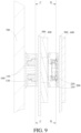
- the circuit board stack structure may include a third circuit board 700, a circuit board assembly, and a second circuit board 500 that are stacked in sequence.
- the third circuit board 700 may be a main board to be used as a mounting base of the circuit board stack structure of this application.
- the second circuit board 500 may be a flexible printed circuit (Flexible Printed Circuit, FPC), and the flexible printed circuit may be arranged in the circuit board assembly.
- FPC Flexible Printed Circuit
- circuit board stack structure Using the circuit board stack structure, independent current paths can be formed between the third circuit board 700 and the circuit board assembly, and between the third circuit board 700 and the second circuit board 500.
- the stack structure arrangement of this application more circuit boards can be laid out without changing a layout area, thereby improving the overall integration and utilization, and further meeting power supply needs of more functional devices.
- the circuit board assembly is first introduced.
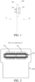
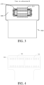
- the circuit board assembly of this application may include a first connector 120, a first circuit board 300, and a second connection base 210 that are stacked in sequence.
- the first circuit board 300 may be a structure such as a flexible printed circuit or a data line, and the first connector 120 and the second connection base 210 may be set as interfaces arranged on two sides of the first circuit board 300, for inputting and outputting of current.
- the first connector 120 may be provided with a second electrical connection portion 121 and a second connection portion 122.
- the second electrical connection portion 121 and the second connection portion 122 can both be set as interfaces to connect to different functional devices.
- the second connection base 210 is provided with a fourth connection portion 211, and the fourth connection portion 211 may also be set as an interface to connect to the second electrical connection portion 121.
- a surface of the first circuit board 300 that faces the first connector 120 may be provided with a third electrical connection portion 311 and a third connection portion 312, and a surface of the first circuit board 300 that faces the second connection base 210 may be provided with a fourth electrical connection portion 321.
- the third connection portion 312 and the second connection portion 122 correspond to each other in position, and are, for example, respectively set as pins and pads, so that the third connection portion 312 can be welded to the second connection portion 122, to establish an electrical connection between the third connection portion 312 and the second connection portion 122.
- a first conducting wire is arranged on the first circuit board 300.
- the first conducting wire can be etched on the first circuit board 300 in a printing manner, or arranged on the first circuit board 300.
- the first conducting wire is connected to the third connection portion 312.
- the first conducting wire is used as a transmission medium for electric energy and can realize electrical conduction to the third connection portion 312.
- the first conducting wire, the third connection portion 312, and the second connection portion 122 can be electrically connected in sequence to form a second path 20.
- a current from an external power supply can be introduced into the first circuit board 300 through the first conducting wire, and then output through the third connection portion 312 and the second connection portion 122 in sequence.
- the second connection portion 122 is a current output end of the second path 20, and the first conducting wire is a current input end of the second path 20.
- the fourth electrical connection portion 321 and the third electrical connection portion 311 correspond to each other in position
- the fourth connection portion 211 and the fourth electrical connection portion 321 correspond to each other in position
- the third electrical connection portion 311 and the second electrical connection portion 121 correspond to each other in position, which are, for example, set as pins or pads, so that the fourth connection portion 211, the fourth electrical connection portion 321, the third electrical connection portion 311, and the second electrical connection portion 121 are electrically connected in sequence to form the first path 10.
- the first conducting wire laid out on the first circuit board 300 does not pass through the fourth electrical connection portion 321 and the third electrical connection portion 311, so that the fourth connection portion 211 can be a current input end of the first path 10, and the second electrical connection portion 121 can be a current output end of the first path 10.
- the third connection portion 312 is set as a "self-use" part of the first circuit board 300, and the first conducting wire arranged on the first circuit board 300 is connected to the third connection portion 312, thereby realizing the conduction of the second path 20.
- the first conducting wire arranged on the first circuit board 300 is isolated from each of the third electrical connection portion 311 and the fourth electrical connection portion 321, that is, the third electrical connection portion 311 and the fourth electrical connection portion 321 are set as a "bridge" part of the first circuit board 300.
- the "bridge” part is used as a transitional link between the preceding and the following, and is not interfered by the first conducting wire arranged inside the first circuit board 300, and the whole formed by the third electrical connection portion 311 and the fourth electrical connection portion 321, that is, the "bridge” part, can connect the fourth connection portion 211 to the second electrical connection portion 121 to form the first path 10.
- the power supply (that is, the second path 20) connected to the first circuit board 300 itself can be conducted, to perform a function of the first circuit board 300 itself.
- other power supplies and functional devices that is, the first path 10.
- the circuit board assembly may further include a transition board 400.
- the transition board 400 can reinforce the first circuit board 300.
- the transition board 400 can be stacked between the first circuit board 300 and the second connection base 210. In this way, the strength of the first circuit board 300 is partially increased, that is, a part of the first circuit board 300 used to mount the transition board 400 is increased in strength. In this way, the circuit board 300 is less likely to undergo deformations such as warping and torsion, thereby preventing the second connection base 210 and the first connector 120 mounted on the circuit board from deviating from the mounting positions due to a deformation.
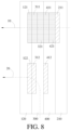
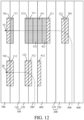
- the transition board 400 should not interfere with the conduction of the second path 20. Therefore, as shown in FIG. 6 and FIG. 7 , a surface of the transition board 400 that faces the second connection base 210 may be provided with a sixth electrical connection portion 421, and a surface of the transition board 400 that faces the first circuit board 300 may be provided with a fifth electrical connection portion 411.
- the sixth electrical connection portion 421, the fifth electrical connection portion 411, the fourth electrical connection portion 321, and the third electrical connection portion 311 may all be set as pads, and correspond to each other in position. In this way, the whole formed by the sixth electrical connection portion 421 and the fifth electrical connection portion 411 can play a role similar to that of the whole formed by the fourth electrical connection portion 321 and the third electrical connection portion 311, that is, the arrangement of the sixth electrical connection portion 421 and the fifth electrical connection portion 411 can be used as a "bridge" part of the transition board 400.
- the "bridge” part is used as a transitional link between the preceding and the following, and can cooperate with the "bridge” part formed by the fourth electrical connection portion 321 and the third electrical connection portion 311 to connect the fourth connection portion 211 to the second electrical connection portion 121.
- the fourth connection portion 211, the sixth electrical connection portion 421, the fifth electrical connection portion 411, the fourth electrical connection portion 321, the third electrical connection portion 311, and the second electrical connection portion 121 may be electrically connected in sequence to form the first path 10.
- the third electrical connection portion 311, the third connection portion 312, and the fourth electrical connection portion 321 are each provided with a plurality of pads.
- the pads of the third electrical connection portion 311 and the pads of the fourth electrical connection portion 321 correspond to each other respectively and are connected in sequence.
- the pads of the third electrical connection portion 311 and the pads of the fourth electrical connection portion 321 form a plurality of electrode pillars running through the first circuit board 300, or an electric wire is arranged between the pads of the third electrical connection portion 311 and the pads of the fourth electrical connection portion 321.
- the second electrical connection portion 121 and the second connection portion 122 may be each provided with a plurality of pins.
- the pins of the second electrical connection portion 121 and the pads of the third electrical connection portion 311 correspond to each other respectively and connected in sequence.
- the pins of the second connection portion 122 and the pads of the third connection portion 312 correspond to each other respectively and connected to each other.
- the first connector 120 is welded to the first circuit board 300 through the connection between the pads and the pins, such as using SMT patch or DIP insertion welding.
- the foregoing design of the pads and the pins can not only ensure a firm connection between the first connector 120, the first circuit board 300, the transition board 400, and the second connection base 210 through welding, but also ensure effective electrical conduction of the second path 20 and effective electrical conduction of the first path 10.
- the fifth electrical connection portion 411 and the sixth electrical connection portion 421 may also be each provided with a plurality of pads, and the pads of the fifth electrical connection portion 411 and the pads of the sixth electrical connection portion 421 correspond to each other respectively and connected in sequence.
- the pads of the fifth electrical connection portion 411 and the pads of the sixth electrical connection portion 421 form a plurality of electrode pillars running through the transition board 400, or an electric wire is arranged between the pads of the fifth electrical connection portion 411 and the pads of the sixth electrical connection portion 421.
- the fourth connection portion 211 may be provided with a plurality of pins, and the pads of the sixth electrical connection portion 421 and the pins of the fourth connection portion 211 correspond to each other respectively and are connected in sequence, so that the second connection base 210 and the transition board 400 are welded to each other.
- the pads of the fourth electrical connection portion 321 and the pads of the fifth electrical connection portion 411 correspond to each other respectively and are connected in sequence, so that the first circuit board 300 and the transition board 400 are welded to each other.
- the first connector 120, the first circuit board 300, the transition board 400, and the second connection base 210 are stacked in sequence through welding to form the circuit board assembly.
- the pins of the second electrical connection portion 121, the pads of the third electrical connection portion 311, the pads of the fourth electrical connection portion 321, the pads of the fifth electrical connection portion 411, the pads of the sixth electrical connection portion 421, and the pins of the fourth connection portion 211 correspond to each other respectively and connected in sequence to form the first path 10.
- the pins of the second connection portion 122 and the pads of the third connection portion 312 correspond to each other respectively and connected to each other to form the second path 20.
- the transition board 400 may further include a reserved connection portion 412.
- the reserved connection portion 412 may be an electrode pillar running through the transition board 400, to serve as a spare region in which the fifth electrical connection portion 411 and the sixth electrical connection portion 421 are located. If the fifth electrical connection portion 411 and the sixth electrical connection portion 421 are damaged, the transition board 400 can be mounted in a reverse direction to establish a connection relationship between the reserved connection portion 412 and the fourth electrical connection portion 321 and the fourth connection portion 211 to prevent the first path 10 from being disconnected.
- the third circuit board 700, the circuit board assembly, and the second circuit board 500 are stacked in sequence.
- a surface of the third circuit board 700 that faces the circuit board assembly is provided with a first connection base 110.
- the third circuit board 700 is connected to a first connector 120 through the first connection base 110.
- the first connection base 110 is welded to the first connector 120.
- a surface of the second circuit board 500 that faces the circuit board assembly is provided with a second connector 220, and the second circuit board 500 is connected to the second connection base 210 through the second connector 220.
- the second connector 220 is welded to the second connection base 210.
- the third circuit board 700 may be provided with a first receiving portion 701 and a second receiving portion 702.
- the first connection base 110 may be provided with a first electrical connection portion 111 and a first connection portion 112.
- the second connector 220 may be provided with a fifth connection portion 221.
- the second circuit board 500 may be provided with a sixth connection portion 501.
- the sixth connection portion 501, the fifth connection portion 221, the fourth connection portion 211, the sixth electrical connection portion 421, the fifth electrical connection portion 411, the fourth electrical connection portion 321, the third electrical connection portion 311, the second electrical connection portion 121, the first electrical connection portion 111, and the first receiving portion 701 are electrically connected in sequence.
- An electric wire connected to the sixth connection portion 501, such as a second conducting wire may be laid on the second circuit board 500.
- An electric wire connected to the first receiving portion 701, such as a third conducting wire may be laid on the third circuit board 700. In this way, when the second circuit board 500 is connected to the power supply through the second conducting wire, the electric energy can be transmitted to the first receiving portion 701 through the first path 10, and then transmitted to a corresponding functional device through the third conducting wire laid on the third circuit board 700.
- the first conducting wire on the first circuit board 300, the third connection portion 312, the second connection portion 122, the first connection portion 112, and the second receiving portion 702 are electrically connected in sequence.
- an electric wire connected to the second receiving portion 702, such as a fourth conducting wire is laid on the third circuit board 700.
- circuit board stack structure there are two different paths formed in the circuit board stack structure at the same time through stacking, such as the first path and the second path, thereby supplying power to different functional devices, for example, supplying power to a lens and a memory separately, or supplying power to different lenses.
- different functional devices for example, supplying power to a lens and a memory separately, or supplying power to different lenses.
- the first connector 120 is plugged into the first connection base 110.
- the first electrical connection portion 111 and the first connection portion 112 are each provided with a socket, and the second electrical connection portion 121 and the second connection portion 122 are each provided with a plug.
- the first electrical connection portion 111 and the second electrical connection portion 121 are plugged into each other, and the first connection portion 112 and the second connection portion 122 are plugged into each other.
- the first connection base 110 and the first connector 120 form a first board-to-board connector 100.
- the second connector 220 is plugged into the second connection base 210.
- the fourth connection portion 211 is provided with a socket
- the fifth connection portion 221 is provided with a plug
- the fourth connection portion 211 and the fifth connection portion 221 are plugged into each other.
- the second connector 220 and the second connection base 210 form a second board-to-board connector 200.
- matching electrical contacts are arranged between the socket of the first electrical connection portion 111 and the plug of the second electrical connection portion 121, between the socket of the first connection portion 112 and the plug of the second connection portion 122, and between the socket of the fourth connection portion 211 and the plug of the fifth connection portion 221.
- the first board-to-board connector 100 is formed through plugging
- the second board-to-board connector 200 is formed through plugging
- electrical conduction is completed between the matching plugs and sockets through contacting between the electrical contacts, that is, the first board-to-board connector 100 and the second board-to-board connector 200 form an electrical conductor after being formed through plugging, and the structural arrangement of the board-to-board connector is more suitable for the electrical connection of the apparatus of this application.
- the first connection base 110 is provided with a first socket, a first part of the first socket is located at the first electrical connection portion 111, and a second part of the first socket is located at the first connection portion 112.
- the first part of the first socket is in communication with the second part of the first socket.
- the first connector 120 is provided with a first plug, a first part of the first plug is located at the second electrical connection portion 121, and a second part of the first plug is located at the second connection portion 122.
- the first part of the first plug is in communication with the second part of the first plug.
- the first plug is plugged into the first socket, and the first socket and the first plug are provided with matching electrical contacts for the electrical conduction between the first connection base 110 and the first connector 120.
- first electrical connection portion 111 and the first connection portion 112 share the first socket, and the second electrical connection portion 121 and the second connection portion 122 share the first plug, a gap between the first electrical connection portion 111 and the first connection portion 112 and a gap between the second electrical connection portion 121 and the second connection portion 122 can be omitted, further reducing the layout space and improving the utilization of the circuit board stack structure.
- the first receiving portion 701 and the second receiving portion 702 may be each provided with a plurality of pads, and the first electrical connection portion 111 and the first connection portion 112 may be each provided with a plurality of pins.
- the pads of the first receiving portion 701 and the pins of the first electrical connection portion 111 correspond to each other respectively and are connected in sequence, for example, the pins and the pads are welded to each other through SMT patch or DIP insertion, so that the first connection base 110 is welded to the third circuit board 700.
- the sixth connection portion 501 is provided with a plurality of pads, and the fifth connection portion 221 is provided with a plurality of pins.
- the pins of the fifth connection portion 221 and the pads of the sixth connection portion 501 correspond to each other respectively and are connected in sequence, for example, the pins and the pads are welded to each other through SMT patch or DIP insertion, so that the second connector 220 is welded to the second circuit board 500.
- the pins of the first electrical connection portion 111 and the pins of the second electrical connection portion 121 correspond to each other respectively, and the pins of the first connection portion 112 and the pins of the second connection portion 122 correspond to each other respectively.
- the pins of the first electrical connection portion 111 and the pins of the second electrical connection portion 121 can be connected to each other to achieve electrical conduction, and the pins of the first connection portion 112 and the pins of the second connection portion 122 can be connected to each other to achieve electrical conduction.
- the third circuit board 700, the first board-to-board connector 100, the first circuit board 300, the transition board 400, the second board-to-board connector 200, and the second circuit board 500 are stacked in sequence through welding to form the circuit board stack structure.
- the pads of the first receiving portion 701, the pins of the first electrical connection portion 111, the pins of the second electrical connection portion 121, the pads of the third electrical connection portion 311, the pads of the fourth electrical connection portion 321, the pads of the fifth electrical connection portion 411, the pads of the sixth electrical connection portion 421, the pins of the fourth connection portion 211, the pins of the fifth connection portion 221, and the pads of the sixth connection portion 501 correspond to each other respectively and connected in sequence to form the first path 10.
- the pads of the second receiving portion 702, the pins of the first connection portion 112, the pins of the second connection portion 122, and the pads of the third connection portion 312 correspond to each other respectively and connected in sequence to form the second path 20.
- the foregoing design of the pads and the pins can not only ensure a firm connection between the third circuit board 700, the circuit board assembly, and the second circuit board through welding, but also ensure effective electrical conduction of the second path 20 and effective electrical conduction of the first path 10.
- the circuit board stack structure may include a reinforcement board 600.
- the reinforcement board 600 is stacked on a side of the second circuit board 500 that faces away from the second connector 220.
- the arrangement of the reinforcement board 600 can increase the overall strength of the second circuit board 500 and prevent abnormal deformations such as warping and torsion.
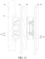
- the third circuit board 700 can be provided with an accommodating hole 710, and at least part of the first connection base 110 is arranged in the accommodating hole 710. This structure can realize at least partial overlapping between the first connection base 110 and the third circuit board 700 in a height direction of stacking, thereby thinning the circuit board stack structure.
- the pads of the first receiving portion 701 and the pads of the second receiving portion 702 may be arranged around the accommodating hole 710, and the pins of the first electrical connection portion 111 and the pins of the first connection portion 112 may be arranged peripherally around the first connection base 110 to achieve a better fit between the two.
- the electronic device disclosed in the embodiments of this application may be a smart phone, a tablet computer, an e-book reader, a wearable device (such as a smart watch, or smart glasses), or the like.
- the electronic device includes the circuit board assembly, and the embodiments of this application do not limit specific types of the electronic device.
Landscapes
- Engineering & Computer Science (AREA)
- Microelectronics & Electronic Packaging (AREA)
- Manufacturing & Machinery (AREA)
- Combinations Of Printed Boards (AREA)
Applications Claiming Priority (2)
| Application Number | Priority Date | Filing Date | Title |
|---|---|---|---|
| CN202110921182.6A CN113677093B (zh) | 2021-08-11 | 2021-08-11 | 电路板组件、电路板堆叠结构及电子设备 |
| PCT/CN2022/110556 WO2023016368A1 (fr) | 2021-08-11 | 2022-08-05 | Ensemble carte de circuit imprimé, structure d'empilement de carte de circuit imprimé et dispositif électronique |
Publications (2)
| Publication Number | Publication Date |
|---|---|
| EP4387401A1 true EP4387401A1 (fr) | 2024-06-19 |
| EP4387401A4 EP4387401A4 (fr) | 2024-11-27 |
Family
ID=78542373
Family Applications (1)
| Application Number | Title | Priority Date | Filing Date |
|---|---|---|---|
| EP22855349.1A Pending EP4387401A4 (fr) | 2021-08-11 | 2022-08-05 | Ensemble carte de circuit imprimé, structure d'empilement de carte de circuit imprimé et dispositif électronique |
Country Status (4)
| Country | Link |
|---|---|
| US (1) | US20240224425A1 (fr) |
| EP (1) | EP4387401A4 (fr) |
| CN (1) | CN113677093B (fr) |
| WO (1) | WO2023016368A1 (fr) |
Families Citing this family (2)
| Publication number | Priority date | Publication date | Assignee | Title |
|---|---|---|---|---|
| CN113677093B (zh) * | 2021-08-11 | 2022-07-22 | 维沃移动通信有限公司 | 电路板组件、电路板堆叠结构及电子设备 |
| CN115440136B (zh) * | 2022-09-28 | 2024-12-17 | 武汉天马微电子有限公司 | 显示模组和显示装置 |
Family Cites Families (16)
| Publication number | Priority date | Publication date | Assignee | Title |
|---|---|---|---|---|
| NL9200117A (nl) * | 1992-01-22 | 1993-08-16 | Du Pont Nederland | Stelsel en connectoren voor het onderling elektrisch verbinden van componentplaten. |
| JP2002252468A (ja) * | 2001-02-26 | 2002-09-06 | Kubota Corp | 多層基板 |
| JP4723178B2 (ja) * | 2003-10-28 | 2011-07-13 | エルピーダメモリ株式会社 | メモリシステム及びメモリモジュール |
| CN101453070B (zh) * | 2007-11-28 | 2012-07-04 | 深圳富泰宏精密工业有限公司 | 连接器及其与电路板的电连接结构 |
| WO2010042591A1 (fr) * | 2008-10-07 | 2010-04-15 | Molex Incorporated | Ensemble tableau de connexions amélioré s’utilisant avec des réseaux de données |
| US20100326704A1 (en) * | 2009-06-30 | 2010-12-30 | Wintek Corporation | Soldering pad layout for flexible printed circuit board |
| US20150208506A1 (en) * | 2012-08-10 | 2015-07-23 | Telefonaktiebolaget L M Ericsson (Publ) | A printed circuit board arrangement and a method for forming electrical connection at a printed circuit board |
| CN104039082B (zh) * | 2014-06-20 | 2018-03-09 | 昆山龙腾光电有限公司 | 一种印刷电路板及使用其的显示装置 |
| US11205867B2 (en) * | 2017-09-15 | 2021-12-21 | Molex, Llc | Grid array connector system |
| US10707600B1 (en) * | 2019-06-28 | 2020-07-07 | Arista Networks, Inc. | Systems with electrical isolation between signal and power domains |
| CN210405971U (zh) * | 2019-08-02 | 2020-04-24 | 维沃移动通信有限公司 | 电路板装置及电子设备 |
| CN113133198A (zh) * | 2019-12-30 | 2021-07-16 | 华为技术有限公司 | 电路板组件和电子设备 |
| CN211184426U (zh) * | 2020-02-24 | 2020-08-04 | 维沃移动通信有限公司 | 一种电路板堆叠结构及电子设备 |
| WO2021184189A1 (fr) * | 2020-03-17 | 2021-09-23 | 深圳市大疆创新科技有限公司 | Structure de carte de circuit imprimé, produit électronique et procédé de préparation pour structure de carte de circuit imprimé |
| CN112261775B (zh) * | 2020-10-09 | 2022-06-07 | Oppo广东移动通信有限公司 | 堆叠式电路板 |
| CN113677093B (zh) * | 2021-08-11 | 2022-07-22 | 维沃移动通信有限公司 | 电路板组件、电路板堆叠结构及电子设备 |
-
2021
- 2021-08-11 CN CN202110921182.6A patent/CN113677093B/zh active Active
-
2022
- 2022-08-05 WO PCT/CN2022/110556 patent/WO2023016368A1/fr not_active Ceased
- 2022-08-05 EP EP22855349.1A patent/EP4387401A4/fr active Pending
-
2024
- 2024-02-06 US US18/434,639 patent/US20240224425A1/en active Pending
Also Published As
| Publication number | Publication date |
|---|---|
| CN113677093A (zh) | 2021-11-19 |
| CN113677093B (zh) | 2022-07-22 |
| EP4387401A4 (fr) | 2024-11-27 |
| US20240224425A1 (en) | 2024-07-04 |
| WO2023016368A1 (fr) | 2023-02-16 |
Similar Documents
| Publication | Publication Date | Title |
|---|---|---|
| CN109599690B (zh) | 一种转接连接器及电连接器组件 | |
| US20240224425A1 (en) | Circuit board assembly, circuit board stack structure, and electronic device | |
| US11817646B2 (en) | Conductive terminal assembly and conductive terminal | |
| CN206962056U (zh) | 电连接器 | |
| CN105932447A (zh) | 金手指连接器、电路板和连接器组件 | |
| KR20120022624A (ko) | 전기 커넥터 및 회로 보드 어셈블리 | |
| CN101369693A (zh) | 电连接器 | |
| CN201667411U (zh) | 电连接器 | |
| KR20200041188A (ko) | 리셉터클 커넥터 | |
| CN204179284U (zh) | 电连接器母头 | |
| WO2008083166A2 (fr) | Connecteur électrique présentant une broche de mise à la terre | |
| CN101826667A (zh) | 双插接面的插座 | |
| CN208045773U (zh) | 具有不同间距的信号端子与接地端子且兼有肋条的连接器 | |
| CN202697021U (zh) | 金手指印制电路板 | |
| CN108512964A (zh) | 移动终端及移动终端的电路板装置 | |
| CN101465487A (zh) | 一种板对板连接器 | |
| US20210296830A1 (en) | Electrical connector | |
| CN210182625U (zh) | 一种用于led显示器的电连接器 | |
| CN219590561U (zh) | 一种光电模块、光电连接器组件及通信单元 | |
| CN203250909U (zh) | 电连接器组合 | |
| CN101465486A (zh) | 电子模块 | |
| CN204947277U (zh) | 组合型插卡式连接器 | |
| KR101321656B1 (ko) | 고속 메모리 카드 어댑터와 소켓용 커넥터 | |
| CN219718584U (zh) | 一种功能板卡及电子设备 | |
| CN218896836U (zh) | 一种插座保护结构及电子设备 |
Legal Events
| Date | Code | Title | Description |
|---|---|---|---|
| STAA | Information on the status of an ep patent application or granted ep patent |
Free format text: STATUS: THE INTERNATIONAL PUBLICATION HAS BEEN MADE |
|
| PUAI | Public reference made under article 153(3) epc to a published international application that has entered the european phase |
Free format text: ORIGINAL CODE: 0009012 |
|
| STAA | Information on the status of an ep patent application or granted ep patent |
Free format text: STATUS: REQUEST FOR EXAMINATION WAS MADE |
|
| 17P | Request for examination filed |
Effective date: 20240105 |
|
| AK | Designated contracting states |
Kind code of ref document: A1 Designated state(s): AL AT BE BG CH CY CZ DE DK EE ES FI FR GB GR HR HU IE IS IT LI LT LU LV MC MK MT NL NO PL PT RO RS SE SI SK SM TR |
|
| REG | Reference to a national code |
Ref country code: DE Ref legal event code: R079 Free format text: PREVIOUS MAIN CLASS: H05K0001140000 Ipc: H01R0012730000 |
|
| DAV | Request for validation of the european patent (deleted) | ||
| DAX | Request for extension of the european patent (deleted) | ||
| A4 | Supplementary search report drawn up and despatched |
Effective date: 20241028 |
|
| RIC1 | Information provided on ipc code assigned before grant |
Ipc: H05K 1/14 20060101ALI20241022BHEP Ipc: H01R 12/71 20110101ALI20241022BHEP Ipc: H01R 12/73 20110101AFI20241022BHEP |