EP4389692A1 - Dispositif et procédé de stockage d'hydrogène - Google Patents
Dispositif et procédé de stockage d'hydrogène Download PDFInfo
- Publication number
- EP4389692A1 EP4389692A1 EP22214665.6A EP22214665A EP4389692A1 EP 4389692 A1 EP4389692 A1 EP 4389692A1 EP 22214665 A EP22214665 A EP 22214665A EP 4389692 A1 EP4389692 A1 EP 4389692A1
- Authority
- EP
- European Patent Office
- Prior art keywords
- shell
- pillar
- core
- hydrogen
- gan
- Prior art date
- Legal status (The legal status is an assumption and is not a legal conclusion. Google has not performed a legal analysis and makes no representation as to the accuracy of the status listed.)
- Withdrawn
Links
Images

Classifications
-
- C—CHEMISTRY; METALLURGY
- C01—INORGANIC CHEMISTRY
- C01B—NON-METALLIC ELEMENTS; COMPOUNDS THEREOF; METALLOIDS OR COMPOUNDS THEREOF NOT COVERED BY SUBCLASS C01C
- C01B3/00—Hydrogen; Gaseous mixtures containing hydrogen; Separation of hydrogen from mixtures containing it; Purification of hydrogen; Reversible storage of hydrogen
- C01B3/0005—Reversible storage of hydrogen, e.g. by hydrogen getters or electrodes
- C01B3/001—Reversible storage of hydrogen, e.g. by hydrogen getters or electrodes characterised by the uptaking media; Treatment thereof
-
- C—CHEMISTRY; METALLURGY
- C01—INORGANIC CHEMISTRY
- C01B—NON-METALLIC ELEMENTS; COMPOUNDS THEREOF; METALLOIDS OR COMPOUNDS THEREOF NOT COVERED BY SUBCLASS C01C
- C01B3/00—Hydrogen; Gaseous mixtures containing hydrogen; Separation of hydrogen from mixtures containing it; Purification of hydrogen; Reversible storage of hydrogen
- C01B3/0005—Reversible storage of hydrogen, e.g. by hydrogen getters or electrodes
- C01B3/001—Reversible storage of hydrogen, e.g. by hydrogen getters or electrodes characterised by the uptaking media; Treatment thereof
- C01B3/0084—Solid storage media characterised by their shape, e.g. porous compacts or hollow particles
-
- C—CHEMISTRY; METALLURGY
- C30—CRYSTAL GROWTH
- C30B—SINGLE-CRYSTAL GROWTH; UNIDIRECTIONAL SOLIDIFICATION OF EUTECTIC MATERIAL OR UNIDIRECTIONAL DEMIXING OF EUTECTOID MATERIAL; REFINING BY ZONE-MELTING OF MATERIAL; PRODUCTION OF A HOMOGENEOUS POLYCRYSTALLINE MATERIAL WITH DEFINED STRUCTURE; SINGLE CRYSTALS OR HOMOGENEOUS POLYCRYSTALLINE MATERIAL WITH DEFINED STRUCTURE; AFTER-TREATMENT OF SINGLE CRYSTALS OR A HOMOGENEOUS POLYCRYSTALLINE MATERIAL WITH DEFINED STRUCTURE; APPARATUS THEREFOR
- C30B25/00—Single-crystal growth by chemical reaction of reactive gases, e.g. chemical vapour-deposition growth
- C30B25/02—Epitaxial-layer growth
- C30B25/18—Epitaxial-layer growth characterised by the substrate
-
- C—CHEMISTRY; METALLURGY
- C30—CRYSTAL GROWTH
- C30B—SINGLE-CRYSTAL GROWTH; UNIDIRECTIONAL SOLIDIFICATION OF EUTECTIC MATERIAL OR UNIDIRECTIONAL DEMIXING OF EUTECTOID MATERIAL; REFINING BY ZONE-MELTING OF MATERIAL; PRODUCTION OF A HOMOGENEOUS POLYCRYSTALLINE MATERIAL WITH DEFINED STRUCTURE; SINGLE CRYSTALS OR HOMOGENEOUS POLYCRYSTALLINE MATERIAL WITH DEFINED STRUCTURE; AFTER-TREATMENT OF SINGLE CRYSTALS OR A HOMOGENEOUS POLYCRYSTALLINE MATERIAL WITH DEFINED STRUCTURE; APPARATUS THEREFOR
- C30B29/00—Single crystals or homogeneous polycrystalline material with defined structure characterised by the material or by their shape
- C30B29/10—Inorganic compounds or compositions
- C30B29/38—Nitrides
-
- C—CHEMISTRY; METALLURGY
- C30—CRYSTAL GROWTH
- C30B—SINGLE-CRYSTAL GROWTH; UNIDIRECTIONAL SOLIDIFICATION OF EUTECTIC MATERIAL OR UNIDIRECTIONAL DEMIXING OF EUTECTOID MATERIAL; REFINING BY ZONE-MELTING OF MATERIAL; PRODUCTION OF A HOMOGENEOUS POLYCRYSTALLINE MATERIAL WITH DEFINED STRUCTURE; SINGLE CRYSTALS OR HOMOGENEOUS POLYCRYSTALLINE MATERIAL WITH DEFINED STRUCTURE; AFTER-TREATMENT OF SINGLE CRYSTALS OR A HOMOGENEOUS POLYCRYSTALLINE MATERIAL WITH DEFINED STRUCTURE; APPARATUS THEREFOR
- C30B29/00—Single crystals or homogeneous polycrystalline material with defined structure characterised by the material or by their shape
- C30B29/10—Inorganic compounds or compositions
- C30B29/40—AIIIBV compounds wherein A is B, Al, Ga, In or Tl and B is N, P, As, Sb or Bi
- C30B29/403—AIII-nitrides
- C30B29/406—Gallium nitride
-
- Y—GENERAL TAGGING OF NEW TECHNOLOGICAL DEVELOPMENTS; GENERAL TAGGING OF CROSS-SECTIONAL TECHNOLOGIES SPANNING OVER SEVERAL SECTIONS OF THE IPC; TECHNICAL SUBJECTS COVERED BY FORMER USPC CROSS-REFERENCE ART COLLECTIONS [XRACs] AND DIGESTS
- Y02—TECHNOLOGIES OR APPLICATIONS FOR MITIGATION OR ADAPTATION AGAINST CLIMATE CHANGE
- Y02E—REDUCTION OF GREENHOUSE GAS [GHG] EMISSIONS, RELATED TO ENERGY GENERATION, TRANSMISSION OR DISTRIBUTION
- Y02E60/00—Enabling technologies; Technologies with a potential or indirect contribution to GHG emissions mitigation
- Y02E60/30—Hydrogen technology
- Y02E60/32—Hydrogen storage
Definitions
- the present inventive concept relates, in general, to a device and a method for hydrogen storage.
- Hydrogen is considered to be a clean and sustainable energy source, and storing hydrogen under ambient conditions is a focus area for research and development. For example, a challenge to the widespread commercialization of fuel cell electric vehicles (FCEVs) and other hydrogen fuel cell applications is how to store the hydrogen in a compact, reliable and cost-effective way.
- FCEVs fuel cell electric vehicles
- One alternative for storing hydrogen includes large-volume systems that store hydrogen in gaseous form. Storage of gaseous hydrogen requires high-pressure tanks. Compressed hydrogen may for example be kept at a tank pressure of around 350-700 bar. Disadvantages of storing compressed gaseous hydrogen include a high energy penalty for compression, which can consume some of the total internal energy of the hydrogen. In addition, expensive carbon fiber wound cylinders may be needed to withstand pressure in the higher ranges.
- Other options for hydrogen storage may include liquefied hydrogen. The boiling point of hydrogen is -252.9°C and to liquefy hydrogen, the temperature needs to be reduced to cryogenic temperatures. The liquefaction process may consume a few tenths of the total internal energy of the hydrogen. It may further be difficult to prevent loss of hydrogen through boil-off when storing it as a liquid. Therefore, a potential loss of energy has to be taken into account when using liquid hydrogen as an energy source.
- hydrogen Compared to other fuels, hydrogen has a higher energy density per mass. However, its low density at ambient temperatures means a lower energy per unit volume. Therefore, the development of storage methods that have the potential for higher energy density is important in order to be able to use hydrogen as an energy source on a larger scale.
- a device for hydrogen storage comprising:
- the inventor has realized that hydrogen may be stored in a solid material.
- Metal or chemical hydrides show high storage capacity but do not satisfy the requirements for the fast kinetics and reversibility.
- Metal-organic frameworks (MOFs) could be used as storage materials owing to their porosity, fast kinetics and reversibility, but high pressure and cryogenics are necessary for the adsorption process because of the weak adsorption energy of hydrogen molecules, mainly via van der Waals interactions, as described in RSC Adv., 2017, 7, 33953 .
- hydrogen may be stored in Mg 3 N 2 or GaN particles.
- such materials may be seen as hydrogen storage materials.
- said hydrogen storage materials may be particularly effective in the form of a shell around the core of a pillar. Such an arrangement may enable hydrogen gas to diffuse into the shell and be stored in the shell or at the interface between the core and the shell. There may be several reasons why the device provides efficient hydrogen storage, as described below.
- the hydrogen storage material may have a large surface to volume ratio when arranged as a shell around the core of a pillar.
- a large surface to volume ratio may result in a large storage capacity.
- Hydrogen storage may be most efficient in the outermost part of the hydrogen storage material, i.e. close to the outer surface of the hydrogen storage material.
- the large surface to volume ratio may e.g. facilitate efficient hydrogen diffusion into the hydrogen storage material.
- the diffusion time may increase, e.g. increase exponentially, with distance into the hydrogen storage material.
- the device facilitates electrical control of the hydrogen storage.
- an electric field may be applied across the shell of the pillar by applying an electrical potential to the core of the pillar.
- Such electrical control may enable reversible hydrogen storage.
- An electric field may be utilized to facilitate the binding and releasing of hydrogen. The electric field may, for example, be applied such that binding of hydrogen is facilitated. The electric field may then be reversed such that the release of hydrogen is facilitated.
- the device facilitates transport of hydrogen.
- Hydrogen may be loaded into the shell in a loading step.
- the device may then be transported, in a transporting step, with the loaded hydrogen.
- Said transport may be safe as the risk of an explosion may be low when the hydrogen is loaded into the shell.
- Hydrogen may then be released from the device in a release step.
- the loading step may comprise:
- Hydrogen may then be adsorbed and/or absorbed by the shell.
- the adsorption or absorption may herein be aided or caused by the first electric field.
- Hydrogen absorbed by the shell may be held by the shell in a volume of the shell, e.g. homogeneously distributed in the shell.
- Hydrogen adsorbed by the shell may be held by the shell on a surface of the shell.
- Said surface of the shell may be an internal surface of the shell, e.g. a surface between two layers of the shell, such as a surface between two crystalline layers of the shell.
- said surface of the shell may be an inner surface of the shell, such as the interface surface between the shell and the core of the pillar.
- said surface of the shell may be an outer surface of the shell.
- the hydrogen may be attracted to the adsorption surface (e.g. internal surface of the shell and/or inner surface of the shell and/or outer surface of the shell) through London dispersion forces.
- the London dispersion forces may form from a sheet of electrons formed at the surface of the materials.
- An electron gas may be formed at the interface between the core of the pillar and the shell of the pillar.
- the electron gas may be a 2-dimensional electron gas.
- the inventor has realized that the 2-dimensional electron gas may provide a potential energy well that is able to bind hydrogen.
- a semiconductor substrate with at least one pillar facilitates the formation of potential energy wells.
- the increased surface and the formation of potential energy wells allows for increased storage capacity.
- the increased storage capacity according to the inventive concept, allows for greater volumetric efficiency and greater mass storage efficiency. Greater volumetric efficiency and greater mass storage efficiency may lead to that the inventive concept can be efficiently implemented in transportation applications.
- the device may be transported in the transporting step.
- the device may e.g. be transported with no electric field applied across the shell of the pillar.
- the hydrogen may still be held by the shell without leaking or only leaking slowly.
- the device may be transported with an electric field applied across the shell of the pillar.
- the release step may comprise: applying a second electric field across the shell of the pillar by applying an electrical potential to the core of the pillar.
- the second electric field may have a direction opposite to the first electric field. Hydrogen may then be released by the shell. The release may herein be aided or caused by the second electric field.
- the semiconductor substrate may comprise any semiconductor material, e.g. silicon, sapphire, silicon carbide, or GaN.
- the semiconductor substrate may be a semiconductor substrate suitable for epitaxial growth. It may be particularly useful with a silicon substrate. Silicon substrates are cheap and there are well developed processing methods for silicon in the semiconductor industry.
- the semiconductor substrate may be a silicon ⁇ 111> substrate or a silicon ⁇ 100> substrate. Such substrates may be particularly suitable for epitaxial growth.
- ⁇ 111> and ⁇ 100> refers to the Miller indices of the substrate surface.
- the semiconductor substrate may be of a different material than the semiconductor material of the core of the pillar.
- the semiconductor substrate material may be silicon, sapphire, or silicon carbide and the material of the core of the pillar may be GaN or AlGaN. Any combination of the above-mentioned semiconductor substrate materials and core materials is possible.
- the semiconductor substrate material and the material of the core of the pillar may be the same material, for example Si.
- the semiconductor substrate material and the material of the core of the pillar may be any other combination of semiconductor materials.
- the pillar may be arranged vertically on the substrate.
- the axis of the pillar may extend in a vertical direction.
- a vertical direction refers to a direction normal to the substrate surface.
- a lateral direction refers to a direction parallel with the substrate surface.
- the device may comprise more than one pillar.
- the device may comprise a plurality of pillars. Said plurality of pillars may be arranged vertically on the substrate.
- the plurality of pillars may be an array of pillars. The number of pillars per square mm may be at least 250 000.
- the pillar may, in principle, have any thickness. However, a diameter of the pillar may advantageously be below 1 micrometer, preferably below 100 nm. The diameter of the pillar herein includes the shell. Thus, the pillar may be thin.
- the surface area of the hydrogen storage material may be increased by increasing the number of pillars on the semiconductor substrate. An increased semiconductor substrate surface area allows for a greater capacity for storing hydrogen. The thinner the pillars are, the more pillars can be fitted on the same semiconductor substrate, leading to a better surface to volume ratio. It is therefore a realization that a thin pillar allows for more pillars and therefore facilitates an increased capacity for storing hydrogen.
- the pillar may, in principle, have any length. However, it may be advantageous with a length above 1 micrometer, such as above 3 micrometers. Such lengths may result in a good surface to volume ratio while being easy to fabricate.
- the core of the pillar may comprise a semiconductor material, e.g. silicon, GaN or AlGaN.
- the shell of the pillar comprises, as previously mentioned, Mg 3 N 2 and/or a plurality of GaN particles.
- the shell encloses the core.
- the shell may enclose the side walls of the pillar.
- the shell may encircle the circumference of the pillar.
- Mg 3 N 2 is also known as magnesium nitride.
- Magnesium nitride may be epitaxially grown both on ⁇ 100> and ⁇ 111 > crystal orientations, e.g. on ⁇ 100> or ⁇ 111> side facets of the core of the pillar.
- Magnesium nitride may, for example, be sputtered, grown by metalorganic vapor deposition, or grown by plasma-assisted molecular beam epitaxy (MBE), e.g. on silicon substrates, e.g. on a silicon pillar.
- MBE plasma-assisted molecular beam epitaxy
- the Mg 3 N 2 shell may be doped, e.g. silicon doped.
- a doped Mg 3 N 2 shell may be utilized as a reversible hydrogen storage material.
- the shell of the pillar may comprise graphitic Mg 3 N 2 .
- graphitic Mg 3 N 2 may intercalate the hydrogen to allow hydrogen storage.
- the Mg and N atoms form a crystalline structure corresponding to graphite.
- Graphitic Mg 3 N 2 may be seen as one or more layers wherein each individual layer has a hexagonal lattice, such as the hexagonal lattice of graphite, and wherein each hexagon of the hexagonal lattice comprises both Mg atoms and N atoms.
- the inventor has realized that the formation of a potential energy well facilitates the binding of hydrogen.
- London dispersion forces in intercalated materials may cause the hydrogen molecules to have a higher binding affinity than that of conventional adsorption by chemisorption or physisorption.
- Physisorption materials adsorb molecular hydrogen via van der Waals interaction, which is usually below 10 kJ. mol -1 .
- Adsorption of hydrogen is favored by London dispersion forces from the electron cloud of the crystal surface.
- the gas density is exp ⁇ V k B T larger inside the potential energy well than outside of the potential energy well, where V is the depth of the potential energy well, k B is Boltzmann's constant and T is the temperature as described in RSC Adv., 2017, 7, 33953, which is included by reference herein.
- the hydrogen storage gravimetric efficiency for graphitic Mg 3 N 2 may be as high as 15.2 weight percent.
- the shell of the pillar may, as an alternative, comprise other crystal structures of Mg 3 N 2 than graphitic Mg 3 N 2 .
- the shell of the pillar may comprise Mg 3 N 2 with a cubic crystal structure, i.e. cubic Mg 3 N 2 .
- Cubic Mg 3 N 2 has a lower in-plane lattice constant than silicon.
- the shell of the pillar may comprise Mg 3 N 2 in the form of a thin-film.
- a thin-film may be a monolayer of molecules. Alternatively, the thin-film may comprise several layers of molecules.
- the thin-film may, for example, be sputtered, grown by plasma-assisted MBE, or grown by metalorganic vapor deposition.
- a thin-film may have a thickness below e.g. 1 micrometer, such as below 100 nm, such as below 10 nm.
- the shell may comprise a second thin film, in addition to the Mg 3 N 2 thin-film.
- the second thin-film may e.g. comprise gallium nitride.
- the second-thin film may comprise Mg (x) Ga (1-x) N (y) , and/or Ga 12 N 12 , and/or Ga 24 N 24 , and/or MgGa 11 N 12 .
- a thin-film of gallium nitride and/or Mg (x) Ga (1-x) N (y) , and/or Ga 12 N 12 , and/or Ga 24 N 24 , and/or MgGa 11 N 12 may be used in a shell wherein the shell does not comprise Mg 3 N 2 or GaN particles.
- Such a shell may still have advantages similar to those discussed in conjunction with the first aspect of the invention.
- GaN particles may herein be construed as any kind of roughness or perturbation of GaN on a lateral surface of the pillars.
- the GaN particles may be nanocrystals.
- a GaN nanocrystal may be seen as a GaN crystalline particle fitting within a sphere with a diameter of 500 nm, or preferably within a sphere with a diameter of 100 nm.
- the GaN particles may be formed through epitaxial growth on the core.
- the GaN particles may be formed through Stranski-Krastanov or a Volmer-Weber growth on the core.
- the GaN particles may be formed through sputtering of GaN. Sputtering forms, at least under some conditions, small particles (e.g. nanoparticles, or nanocrystals), resulting in a rough surface.
- the GaN particles may be deposited as aerosols or colloids on the core of the pillar.
- the GaN particles may have a size below 50 nm, preferably below 5 nm.
- the GaN particles may be stacked on top of each other. Stacked GaN particles may be separated by grain boundaries and/or by free space. Stacked GaN particles may form a porous shell. In such a porous shell hydrogen may travel deep into the shell through pores between GaN particles and then be trapped in said GaN particles.
- the shell may comprise a plurality of GaN particles forming a rough surface of the shell, wherein the rough surface of the shell of the pillar has a root mean square roughness larger than 1 nm.
- the root mean square roughness is defined as the quadratic average, or root mean square average of profile height deviations from the mean line. Profile height deviations may be measured e.g. by an atomic force microscope.
- the plurality of GaN particles with the above mentioned surface roughness may form crystals or cage-like structures.
- the GaN particle structures may be formed similar to how quantum dots are formed.
- the binding affinity of the particle formations is high and the structures are arranged to bind hydrogen.
- the cage-effect of the crystal structures of the GaN particles allows for hydrogen storage capacities similar to the hydrogen storage capacity of a buckyball or fullerene. Thus, one or more hydrogen atoms may be stored in each GaN particle.
- the rough surface of the shell of the pillar has a root mean square roughness in the range of 1 nm to 10 nm, or in the range of 1 nm to 5 nm. In such a range the hydrogen storage gravimetric efficiency may be particularly high.
- a shell comprising GaN particles may have a thickness below e.g. 500 nm, such as below 100 nm, such as below 10 nm.
- the shell may have a thickness of less than 10 nm.
- a shell of a thickness less than 10 nm which in this text is referred to as a thin shell, may be advantageous for example when placing the semiconductor substrate and the at least one pillar in an electric field.
- a thin shell may facilitate a large field strength.
- a thin shell may be cost effective as hydrogen may be stored most effectively in the outermost parts of the shell. Thus, it may be unnecessary to use a thick shell if only the outermost part stores hydrogen.
- the semiconductor substrate may have a thickness of 1 mm or more.
- a semiconductor substrate with a thickness of 1 mm or more may advantageously withstand pressure, for example in the manufacturing process, or when using the device.
- the semiconductor substrate may be used as part of a wall in a pressurized container.
- the shell of the pillar may be epitaxially aligned with the core of the pillar.
- the core and the shell are epitaxially aligned they share a crystal periodicity in at least one direction, at least at the interface of the core and the shell.
- the shell of the pillar may, for example, comprise cubic and/or graphitic Mg 3 N 2 and/or GaN particles.
- the core and shell is epitaxially aligned, there may be a low defect density in the shell and/or a low defect density at the interface between the core and shell.
- Defects may be e.g. dislocations. Defects may provide deep states which may have an adverse effect on hydrogen storage. Thus, a low defect density may improve hydrogen storage, e.g. improve the hydrogen storage gravimetric efficiency.
- the core of the at least one pillar may comprise silicon and/or gallium nitride and/or aluminum nitride and/or aluminum gallium nitride.
- the crystal orientations of the material of the core of the at least one pillar may for example be ⁇ 100> or ⁇ 111>.
- the core of the pillar may be epitaxially aligned with the semiconductor substrate.
- the core of the pillar may comprise the same material as the substrate.
- the core of the pillar may be made of silicon while the substrate is also made of silicon. Such silicon cores may be etched out of the substrate.
- the core of the pillar may be made of another material than the substrate.
- the core of the pillar may be made of and/or gallium nitride and/or aluminum nitride and/or aluminum gallium nitride while the substrate is made of silicon.
- the at least one pillar may comprise a heterojunction, wherein the heterojunction is configured to form an electron gas.
- the heterojunction may be configured to form the electron gas by band bending.
- the electron gas may be formed at the interface between the core of the pillar and the shell of the pillar.
- the electron gas facilitates the formation of the potential energy well, previously mentioned, such that hydrogen is bound by London dispersion forces. Thus, hydrogen may be bound to the heterojunction.
- the heterojunction may be formed at the interface between the core and the shell.
- the heterojunction may be formed at the interface between the core and a Mg 3 N 2 shell or between the core and one or more GaN particles of the shell.
- the device may comprise a flow channel, the flow channel being configured to pass a flow of hydrogen gas, wherein the at least one pillar is arranged in the flow channel, the device further comprising at least two electrodes, the at least two electrodes being configured to apply an electric field between the core of the pillar and the hydrogen gas in the flow channel.
- the electric field may control the binding and release of hydrogen.
- the electric field may be used to lower the depth of the potential energy well to release the hydrogen gas, or increase the depth of the same potential energy well for binding hydrogen gas.
- a method for producing a device for hydrogen storage comprising:
- the layer of semiconductor material may be provided by epitaxial growth, e.g. by metalorganic vapor deposition, or by sputtering.
- the method may also include that the core of the pillar is lattice mismatched to GaN material and GaN particles are provided as the shell around the core of the at least one pillar by epitaxial growth in a Stranski-Krastanov or a Volmer-Weber growth mode.
- the GaN particles may be formed by strain driven self-assembly.
- the GaN particles may be quantum dots.
- Self-assembled GaN particles may provide a high particle density and/or small particles and/or a suitable surface roughness. This may be beneficial for providing efficient hydrogen storage.
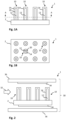
- Fig. 1 A and B illustrate cross sections of a device 1.
- Fig. 1A is a side view of a cross section of the device 1.
- Fig. 1B is a top view of a cross section of the same device 1, wherein the cross section is a cross section along line A-A in Fig. 1A .
- the illustrated device 1 comprises a semiconductor substrate 2 on which a plurality of pillars 10 are arranged.
- Each pillar 10 comprises a core 12 and a shell 14.
- the core 12 and shell 14 may have a circular cross section, as illustrated in Fig. 1B .
- the core 12 and shell 14 may have a cross section of another shape, e.g. hexagonal.
- the shell 14 encloses the core, e.g. by extending over the lateral surfaces of the core 12.
- the shell 14 may additionally, as illustrated, extend over a top surface of the core 12.
- the Mg 3 N 2 and/or the GaN particles 16 of the shell 14 may cover lateral surfaces of the core 12.
- the Mg 3 N 2 and/or the GaN particles 16 of the shell 14 may cover lateral surfaces of the core 12 fully or partially.
- the Mg 3 N 2 and/or the GaN particles 16 of the shell 14 may cover at least 30%, such as at least 70%, of the surface area of the lateral surfaces of the core 12.
- the core 12 and shell 14 may comprise different materials.
- the interface between the core 12 and shell 14 may form a heterojunction 20.
- Said heterojunction 20 may be configured to form an electron gas.
- the core 12 may be made of AlGaN while the shell 14 is made of GaN, or vice versa.
- an electron gas may form.
- Said electron gas may be seen as a two-dimensional electron gas wrapped around the core 12.
- the heterojunction 20 may be formed at the interface between the core 12 and a Mg 3 N 2 shell or between the core and one or more GaN particles of the shell 14.
- Fig. 2 illustrates a cross section of a device 1 comprising a flow channel 30, the flow channel 30 being configured to pass a flow 32 of hydrogen gas, wherein the at least one pillar 10 is arranged in the flow channel 30.
- the device 1 further comprises two electrodes 34 configured to apply an electric field between the core 12 of the pillar 10 and the hydrogen gas in the flow channel 30.
- the flow channel 30 may be any form of pipe, box, or container through which a hydrogen flow can pass.
- the flow channel 30 may comprise walls 36 configured to prevent hydrogen gas from escaping.
- One electrode 34 may be arranged on the substrate 2, e.g. on the back side of the substrate 2.
- Another electrode 34 may be arranged at a different location of the flow channel 30, e.g. on a wall 36 of the flow channel 30.
- an electric field may be applied across the shell 14 of each pillar 10.
- the substrate 2 and/or the core 12 may herein be doped such that a large part of the potential drop falls over the shell 14, whereby the electric field in the shell 14 becomes large.
- the flow channel 30 may be configured such that the substrate 2 with the pillars 10 may be removed.
- the shells 14 of the pillars 10 may be loaded with hydrogen in the flow channel 30, e.g. in the above mentioned loading step, by applying a first electric field.
- the substrate 2 with the pillars 10 may then be removed and transported elsewhere.
- the hydrogen stored in the shells 14 of the pillars 10 may then be released, e.g. in the above mentioned release step.
- the substrate 2 with pillars 10 may be placed in another flow channel 30 and a second electric field may be applied across the shells 14 of the pillars 10.
- the second electric field may have a direction opposite to the first electric field.
- they may stay in the same flow channel 30 for both the loading and release step.
- the substrate 2 may have a thickness of 1 mm or more. This may be advantageous if there is a pressure difference between the front side and the back side of the substrate 2. For example, if the substrate 2 forms part of a wall 36 of the flow channel 30.
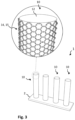
- Fig. 3 illustrates a device 1 in perspective view.
- the shell 14 of the pillars 10 of the illustrated device 1 comprises graphitic Mg 3 N 2 .
- the illustrated pillar 10 has a shell 14 comprising a single layer 17 of graphitic Mg 3 N 2 which is wrapped around the core 12 of the pillar 10.
- the pillar 10 may have a shell 14 comprising multi-layer graphitic Mg 3 N 2 .
- Each individual layer 17 of graphitic Mg 3 N 2 has a hexagonal lattice, similar to the hexagonal lattice of graphite.
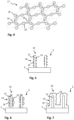
- a layer 17 of graphitic Mg 3 N 2 is illustrated in Fig. 4 , wherein magnesium atoms 18 are illustrated with a dotted texture and nitrogen atoms 19 are illustrated white.
- the dashed square lattice is a guide to the eye.
- the shell 14 may comprise other forms of Mg 3 N 2 , e.g. cubic Mg 3 N 2 .
- Figs 5-7 illustrates that the shell 14 may comprise GaN particles 16.
- Figs 5-7 illustrates cross sections of devices 1 seen in side-view.
- the GaN particles 16 may be scattered on the lateral surfaces of the core 12 and not cover the full surface area of the lateral surfaces of the core 12, as seen in Figs 5-6 .
- the GaN particles 16 may e.g. cover at least 30% or at least 70% of the surface area of the lateral surfaces of the core 12.
- the GaN particles 16 may cover the full surface area of the lateral surfaces of the core 12, as seen in Fig. 7 .
- the GaN particles 16 may be grown epitaxially on the lateral surfaces of the core 12.
- the GaN particles 16 may be grown epitaxially in the Stranski-Krastanov or the Volmer-Weber growth mode.
- Such GaN particles 16 may be lattice mismatched to the core 12 and form by strain driven self-assembly.
- Such GaN particles 16 may have the shape of pyramids, truncated pyramids, or domes.
- Fig. 5 illustrates how GaN particles 16 with a pyramidal shape may look in cross section.
- Fig. 8 illustrates that multiple shells 14 may be used.
- Fig. 8 a cross section of a device 1 in a side-view.
- the illustrated device 1 comprises a first 14' and a second 14" shell.
- the first shell 14' may be a Mg 3 N 2 shell.
- the second shell 14" may be a shell comprising GaN particles 16.
- Fig. 9 shows a flow chart of a method 100 for producing a device 1 according to the first aspect.
- a layer of semiconductor material is provided S102 on the semiconductor substrate 2.
- the layer of semiconductor material may be provided S102 by epitaxial growth.
- the core 12 of the at least one pillar 10 is then formed S104 by plasma etching the layer of semiconductor material with a chlorine plasma.
- the layer of semiconductor material may be patterned by lithographic means, e.g. by nanoimprint lithography or photolithography, and etched to form columns which later will become the cores 12 of the pillars 10.
- Mg 3 N 2 or GaN particles 16 are provided S106 as the shell 14 around the core 12 of the at least one pillar 10. This is done by sputtering or metalorganic vapor deposition.
- the core 12 of the pillar 10 may be lattice mismatched to GaN material.
- the core 12 of the pillar 10 may comprise another material than GaN.
- GaN particles 16 may then be provided S106 as the shell 14 around the core 12 of the at least one pillar 10 by epitaxial growth in a Stranski-Krastanov or a Volmer-Weber growth mode.
- said monolayers may rearrange in a self-assembly process to form quantum dots.
- Said quantum dots may be seen as GaN particles 16 forming a rough surface.
- the quantum dots of the shell 14 may be self-assembled quantum dots.
- the quantum dots may e.g. be Stranski-Krastanov quantum dots.
- the shell 14 may, in addition to the quantum dots, comprise a wetting layer.
- the quantum dots of the shell 14 may be Volmer-Weber quantum dots.
- Self-assembled quantum dots may provide a high quantum dot density and/or small quantum dots. This may be beneficial for enabling efficient hydrogen storage.
- GaN particles 16 are provided by means other than Stranski-Krastanov or a Volmer-Weber growth.
- GaN particles 16 may be provided as small droplets sputtered onto the lateral sides of the etched columns.
- GaN particles 16 may be provided as aerosols or colloids deposited onto the lateral sides of the etched columns.
Landscapes
- Chemical & Material Sciences (AREA)
- Organic Chemistry (AREA)
- Engineering & Computer Science (AREA)
- Inorganic Chemistry (AREA)
- Chemical Kinetics & Catalysis (AREA)
- Crystallography & Structural Chemistry (AREA)
- Materials Engineering (AREA)
- Metallurgy (AREA)
- Combustion & Propulsion (AREA)
- General Chemical & Material Sciences (AREA)
- Hydrogen, Water And Hydrids (AREA)
Priority Applications (8)
| Application Number | Priority Date | Filing Date | Title |
|---|---|---|---|
| EP22214665.6A EP4389692A1 (fr) | 2022-12-19 | 2022-12-19 | Dispositif et procédé de stockage d'hydrogène |
| TW114129632A TW202543723A (zh) | 2022-12-19 | 2023-12-06 | 儲氫裝置和儲氫方法 |
| TW112147548A TWI895869B (zh) | 2022-12-19 | 2023-12-06 | 儲氫裝置和儲氫方法 |
| KR1020257024008A KR20250127117A (ko) | 2022-12-19 | 2023-12-08 | 수소 저장을 위한 장치 및 방법 |
| JP2025535169A JP2025541389A (ja) | 2022-12-19 | 2023-12-08 | 水素貯蔵のための装置および方法 |
| EP23820939.9A EP4638345A1 (fr) | 2022-12-19 | 2023-12-08 | Dispositif et procédé de stockage d'hydrogène |
| CN202380085922.4A CN120379923A (zh) | 2022-12-19 | 2023-12-08 | 用于氢储存的装置和方法 |
| PCT/EP2023/084990 WO2024132603A1 (fr) | 2022-12-19 | 2023-12-08 | Dispositif et procédé de stockage d'hydrogène |
Applications Claiming Priority (1)
| Application Number | Priority Date | Filing Date | Title |
|---|---|---|---|
| EP22214665.6A EP4389692A1 (fr) | 2022-12-19 | 2022-12-19 | Dispositif et procédé de stockage d'hydrogène |
Publications (1)
| Publication Number | Publication Date |
|---|---|
| EP4389692A1 true EP4389692A1 (fr) | 2024-06-26 |
Family
ID=84541650
Family Applications (2)
| Application Number | Title | Priority Date | Filing Date |
|---|---|---|---|
| EP22214665.6A Withdrawn EP4389692A1 (fr) | 2022-12-19 | 2022-12-19 | Dispositif et procédé de stockage d'hydrogène |
| EP23820939.9A Pending EP4638345A1 (fr) | 2022-12-19 | 2023-12-08 | Dispositif et procédé de stockage d'hydrogène |
Family Applications After (1)
| Application Number | Title | Priority Date | Filing Date |
|---|---|---|---|
| EP23820939.9A Pending EP4638345A1 (fr) | 2022-12-19 | 2023-12-08 | Dispositif et procédé de stockage d'hydrogène |
Country Status (6)
| Country | Link |
|---|---|
| EP (2) | EP4389692A1 (fr) |
| JP (1) | JP2025541389A (fr) |
| KR (1) | KR20250127117A (fr) |
| CN (1) | CN120379923A (fr) |
| TW (2) | TWI895869B (fr) |
| WO (1) | WO2024132603A1 (fr) |
Citations (2)
| Publication number | Priority date | Publication date | Assignee | Title |
|---|---|---|---|---|
| US20060060866A1 (en) * | 2000-03-14 | 2006-03-23 | Toyoda Gosel Co., Ltd. | Group III nitride compound semiconductor devices and method for fabricating the same |
| EP4082037A1 (fr) * | 2019-12-26 | 2022-11-02 | Aledia | Dispositif pour traitement par laser et procédé de traitement au laser |
Family Cites Families (3)
| Publication number | Priority date | Publication date | Assignee | Title |
|---|---|---|---|---|
| US6672077B1 (en) * | 2001-12-11 | 2004-01-06 | Nanomix, Inc. | Hydrogen storage in nanostructure with physisorption |
| WO2008112650A2 (fr) * | 2007-03-15 | 2008-09-18 | Yazaki Corporation | Condensateurs comprenant des assemblages organisés de composés carbonés et non carbonés |
| WO2016183678A1 (fr) * | 2015-05-19 | 2016-11-24 | The Royal Institution For The Advancement Of Learning/Mcgill University | Procédés et systèmes de collecte d'énergie solaire et stockage réversible d'hydrogène |
-
2022
- 2022-12-19 EP EP22214665.6A patent/EP4389692A1/fr not_active Withdrawn
-
2023
- 2023-12-06 TW TW112147548A patent/TWI895869B/zh active
- 2023-12-06 TW TW114129632A patent/TW202543723A/zh unknown
- 2023-12-08 EP EP23820939.9A patent/EP4638345A1/fr active Pending
- 2023-12-08 CN CN202380085922.4A patent/CN120379923A/zh active Pending
- 2023-12-08 KR KR1020257024008A patent/KR20250127117A/ko active Pending
- 2023-12-08 WO PCT/EP2023/084990 patent/WO2024132603A1/fr not_active Ceased
- 2023-12-08 JP JP2025535169A patent/JP2025541389A/ja active Pending
Patent Citations (2)
| Publication number | Priority date | Publication date | Assignee | Title |
|---|---|---|---|---|
| US20060060866A1 (en) * | 2000-03-14 | 2006-03-23 | Toyoda Gosel Co., Ltd. | Group III nitride compound semiconductor devices and method for fabricating the same |
| EP4082037A1 (fr) * | 2019-12-26 | 2022-11-02 | Aledia | Dispositif pour traitement par laser et procédé de traitement au laser |
Non-Patent Citations (3)
| Title |
|---|
| MYERS S M ET AL: "Diffusion, release, and uptake of hydrogen in magnesium-doped gallium nitride: Theory and experiment", JOURNAL OF APPLIED PHYSICS, AMERICAN INSTITUTE OF PHYSICS, 2 HUNTINGTON QUADRANGLE, MELVILLE, NY 11747, vol. 89, no. 6, 15 March 2001 (2001-03-15), pages 3195 - 3202, XP012053108, ISSN: 0021-8979, DOI: 10.1063/1.1347410 * |
| NABI GHULAM: "Photoluminescence and hydrogen storage properties of gallium nitride hexagonal micro-bricks - ScienceDirect", MATERIALS LETTERS, vol. 79, 15 July 2012 (2012-07-15), pages 212 - 215, XP093048468 * |
| RSC ADV., vol. 7, 2017, pages 33953 |
Also Published As
| Publication number | Publication date |
|---|---|
| KR20250127117A (ko) | 2025-08-26 |
| EP4638345A1 (fr) | 2025-10-29 |
| JP2025541389A (ja) | 2025-12-18 |
| TWI895869B (zh) | 2025-09-01 |
| TW202426121A (zh) | 2024-07-01 |
| TW202543723A (zh) | 2025-11-16 |
| WO2024132603A1 (fr) | 2024-06-27 |
| CN120379923A (zh) | 2025-07-25 |
Similar Documents
| Publication | Publication Date | Title |
|---|---|---|
| mana Al-Anazy et al. | Study of alkaline metals hydrides RbXH3 (X= Mg/Ca/Sr/Ba) for green energy and hydrogen storage applications | |
| US6672077B1 (en) | Hydrogen storage in nanostructure with physisorption | |
| Ohtomo et al. | Structure and optical properties of ZnO/Mg 0.2 Zn 0.8 O superlattices | |
| Li et al. | Effects of the matrix on self-organization of InAs quantum nanostructures grown on InP substrates | |
| Kundu et al. | Novel permeable material “yttrium decorated zeolite templated carbon” for hydrogen storage: Perspectives from density functional theory | |
| Adelmann et al. | Nucleation and growth of GaN∕ AlN quantum dots | |
| Xu et al. | Atomic structures and mechanical properties of single-crystal GaN nanotubes | |
| EP4389692A1 (fr) | Dispositif et procédé de stockage d'hydrogène | |
| KR20080052321A (ko) | 가스 저장 매체, 가스 저장 장치 및 그 저장 방법 | |
| Kovalevski et al. | TEM study of structure of graphene layers in shungite carbon | |
| JP2004261739A (ja) | 水素吸蔵複合材料 | |
| Jacobsson et al. | Crystal structure tuning in GaAs nanowires using HCl | |
| WO2006104274A1 (fr) | Structure de stockage d’hydrogene | |
| Kesaria et al. | Spontaneous formation of GaN nanostructures by molecular beam epitaxy | |
| Nechaev | The high-density hydrogen carrier intercalation in graphane-like nanostructures, relevance to its on-board storage in fuel-cell-powered vehicles | |
| JP5005941B2 (ja) | 水素貯蔵体 | |
| Singh et al. | Absorption and adsorption-based storage of hydrogen as a fuel | |
| Thamm et al. | Morphology of GaN Surfaces and GaN/(Al, Ga) N Interfaces Grown on 6H‐SiC (0001) by Reactive Molecular Beam Epitaxy | |
| US8673436B2 (en) | Nanoengineered material for hydrogen storage | |
| Glas | Heterostructures and strain relaxation in semiconductor nanowires | |
| Matsumoto et al. | Decomposition of magnesium hydride fiber observed using TEM and in-situ AFM | |
| Tyagi | Interlayer effect on the hydrogen uptake in Vanadium films: Stress development, surface topography and optical behavior changes | |
| Hu | Stress evolution during growth on InAs on GaAs measured by an in-situ cantilever beam setup | |
| Adelung et al. | face phase transition at the SnrGe 111 63= 63R308-a interface Ž. 162–163 2000 48 | |
| Norman et al. | The nature and origin of lateral composition modulations in short-period strained-layer superlattices |
Legal Events
| Date | Code | Title | Description |
|---|---|---|---|
| PUAI | Public reference made under article 153(3) epc to a published international application that has entered the european phase |
Free format text: ORIGINAL CODE: 0009012 |
|
| STAA | Information on the status of an ep patent application or granted ep patent |
Free format text: STATUS: THE APPLICATION HAS BEEN PUBLISHED |
|
| AK | Designated contracting states |
Kind code of ref document: A1 Designated state(s): AL AT BE BG CH CY CZ DE DK EE ES FI FR GB GR HR HU IE IS IT LI LT LU LV MC ME MK MT NL NO PL PT RO RS SE SI SK SM TR |
|
| STAA | Information on the status of an ep patent application or granted ep patent |
Free format text: STATUS: THE APPLICATION IS DEEMED TO BE WITHDRAWN |
|
| 18D | Application deemed to be withdrawn |
Effective date: 20250103 |