EP4389945A1 - Procédé de fabrication d'un élément en nano ou microfeuilles à l'aide d'une couche de support à motifs - Google Patents
Procédé de fabrication d'un élément en nano ou microfeuilles à l'aide d'une couche de support à motifs Download PDFInfo
- Publication number
- EP4389945A1 EP4389945A1 EP22216615.9A EP22216615A EP4389945A1 EP 4389945 A1 EP4389945 A1 EP 4389945A1 EP 22216615 A EP22216615 A EP 22216615A EP 4389945 A1 EP4389945 A1 EP 4389945A1
- Authority
- EP
- European Patent Office
- Prior art keywords
- nano
- micro
- layer
- sheet
- sheet layer
- Prior art date
- Legal status (The legal status is an assumption and is not a legal conclusion. Google has not performed a legal analysis and makes no representation as to the accuracy of the status listed.)
- Withdrawn
Links
Images




Classifications
-
- C—CHEMISTRY; METALLURGY
- C01—INORGANIC CHEMISTRY
- C01B—NON-METALLIC ELEMENTS; COMPOUNDS THEREOF; METALLOIDS OR COMPOUNDS THEREOF NOT COVERED BY SUBCLASS C01C
- C01B32/00—Carbon; Compounds thereof
- C01B32/15—Nano-sized carbon materials
- C01B32/182—Graphene
- C01B32/184—Preparation
- C01B32/19—Preparation by exfoliation
-
- C—CHEMISTRY; METALLURGY
- C01—INORGANIC CHEMISTRY
- C01B—NON-METALLIC ELEMENTS; COMPOUNDS THEREOF; METALLOIDS OR COMPOUNDS THEREOF NOT COVERED BY SUBCLASS C01C
- C01B32/00—Carbon; Compounds thereof
- C01B32/15—Nano-sized carbon materials
- C01B32/182—Graphene
- C01B32/194—After-treatment
-
- C—CHEMISTRY; METALLURGY
- C25—ELECTROLYTIC OR ELECTROPHORETIC PROCESSES; APPARATUS THEREFOR
- C25D—PROCESSES FOR THE ELECTROLYTIC OR ELECTROPHORETIC PRODUCTION OF COATINGS; ELECTROFORMING; APPARATUS THEREFOR
- C25D1/00—Electroforming
- C25D1/006—Nanostructures, e.g. using aluminium anodic oxidation templates [AAO]
-
- C—CHEMISTRY; METALLURGY
- C25—ELECTROLYTIC OR ELECTROPHORETIC PROCESSES; APPARATUS THEREFOR
- C25D—PROCESSES FOR THE ELECTROLYTIC OR ELECTROPHORETIC PRODUCTION OF COATINGS; ELECTROFORMING; APPARATUS THEREFOR
- C25D1/00—Electroforming
- C25D1/20—Separation of the formed objects from the electrodes with no destruction of said electrodes
-
- C—CHEMISTRY; METALLURGY
- C25—ELECTROLYTIC OR ELECTROPHORETIC PROCESSES; APPARATUS THEREFOR
- C25D—PROCESSES FOR THE ELECTROLYTIC OR ELECTROPHORETIC PRODUCTION OF COATINGS; ELECTROFORMING; APPARATUS THEREFOR
- C25D17/00—Constructional parts, or assemblies thereof, of cells for electrolytic coating
- C25D17/002—Cell separation, e.g. membranes, diaphragms
-
- C—CHEMISTRY; METALLURGY
- C25—ELECTROLYTIC OR ELECTROPHORETIC PROCESSES; APPARATUS THEREFOR
- C25D—PROCESSES FOR THE ELECTROLYTIC OR ELECTROPHORETIC PRODUCTION OF COATINGS; ELECTROFORMING; APPARATUS THEREFOR
- C25D17/00—Constructional parts, or assemblies thereof, of cells for electrolytic coating
- C25D17/10—Electrodes, e.g. composition, counter electrode
- C25D17/12—Shape or form
Definitions
- Graphene is a material formed by only a single layer of carbon atoms that are covalently bonded together in a repeating pattern of hexagons.
- graphene is increasingly used in many electronic devices such as biosensors, transistors and integrated circuits, e.g. CMOS-based microchips.
- Applications for which such graphene devices can be used include for example consumer electronics, medical technology, automotive engineering, optics, telecommunications, batteries, space technology, and many more.
- the approach of growth substrate etching has disadvantages, because it leads to i) polymer contamination of the thin sheet materials, ii) dissolution & thereby the loss of the growth substrate, iii) influences the process reproducibility, and iv) generates toxic chemical byproducts.
- the etching process is time-consuming, meaning that it can take up-to 3 to 4 hours to etch a copper foil having a thickness of approx. ⁇ 25 ⁇ m (area ⁇ 4cm 2 ) using a 50 mM of ammonium persulphate-based copper etchant solution.
- a possible, but in practice not suitable way to delaminate the thin sheet material from the growth substrate is by means of a physical peel-off.
- a physical peel-off is not feasible, as it can lead to sample damage and the thin films can adhere to their growth substrates.
- a delamination method is disclosed which is based on a physical separation of the respective layer in combination with a water penetration effect.
- protons can diffuse through the thin sheet material or percolate from the sides to form hydrogen bubbles at the interface of the growth substrate and the thin sheet material of the electrolytic cell thereby providing a delaminating effect, which leads to the detachment of the thin sheet material from its growth substrate.
- electrochemical delamination via an electrolysis process is a viable technique to rapidly release thin sheet material films from their growth substrates within a few minutes only.
- delamination of the thin sheet material from the growth substrate by means of electrolysis is a particularly fast technique to transfer 2D thin materials from their growth substrates to the target device.
- the nano- or micro-sheet layer For transferring the nano- or micro-sheet layer, i.e. the thin sheet material or thin films, to the target substrate, the nano- or micro-sheet layer must be given some structural stability, which is usually achieved by the attachment of a support layer.
- the support layer is used for the transfer and removed after the attachment of the nano- or micro-sheet layer to the target substrate.
- the present invention thus provides a method for producing a nano- or micro-sheet element, the nano- or micro-sheet element particularly being made of graphene and/or other sheet-materials, such as metal thin films, nano-structures and insulating thin films, on the basis of a laminate comprising a growth substrate, a nano- or micro-sheet layer and a support layer, the nano- or micro-sheet layer being adapted to form the nano- or micro-sheet element, wherein the method comprises at least the step of electrochemical delamination of the laminate by means of electrolysis in such a way, that the growth substrate is separated from the nano- or micro-sheet layer and the support layer.
- the production process can be considerably facilitated and made faster.
- the nano- or micro-sheet layer and the nano- or micro-sheet element are preferably, but not necessarily made of graphene.
- the nano- or micro-sheet layer and the nano- or micro-sheet element could for example also be made of hexagonal boron nitride or from any other material.
- the nano- or micro-sheet layer and the nano- or micro-sheet element could also be made of other thin sheet materials, such as thin films, herein referred to fragile plastic films, polymer films, thermally evaporated or sputter deposited thin metal films, micro-stamps, micro-molds, micro-patterns (deposited via catalytic printing) of polymer films or plastic films, which also require delamination from their growth substrate.
- the nano- or micro-sheet layer and the support layer one or more additional layers are present in the laminate.
- the nano- or micro-sheet layer is preferably arranged between the growth substrate and the support layer. Prior to delamination, the layers of the laminate are usually bonded together over their entire surface.
- the nano- or micro-sheet layer is preferably attached, usually directly, to the growth substrate.
- the support layer is preferably attached, directly or indirectly, to the nano- or micro-sheet layer.
- the laminate preferably has the form of a wafer as it is often used in the semiconductor-industry.
- a patterning of the support layer is carried out prior to the step of electrochemical delamination.
- a lithographic patterning it can particularly be an ultra violet (UV)-lithographic patterning.
- UV-lithographic techniques allow for patterning of the support layer directly on the nano- or micro-sheet layer present on the growth substrate.
- the patterning can also be effected by means of laser ablation or laser cutting, or it can be due to a particular physical placement of one or several parts of the support layer on the nano- or micro-sheet layer.
- pre-patterned support layers can be adhered directly onto the nano- or micro-sheet layer on the growth substrate with the help of thermal heating.
- the target substrate can for example be made of glass, polyimide or plastic. It can be in the form of e.g. an integrated chip or a flexible substrate.
- the target substrate has one or more electrical contacts.
- the nano- or micro-sheet layer is attached such to the target substrate, that it connects these electrical contacts.
- the target substrate can have a pattern, which can, but does not need to correspond to the pattern of the substrate layer. If the target substrate has a pattern, it can form one or more depressions, which serve to suspend the nano- or micro-sheet layer. The one or more depressions can particularly serve to suspend the nano- or micro-sheet layer between two or more electrical contacts of the target substrate.
- the nano- or micro-sheet layer can have a uniform thickness over its entire surface or it can be structured to have local elevations and/or depressions.
- the depressions can be non-through-going or through-going, i.e. have the form of apertures in the latter case.
- the structure can particularly be provided, in order to distinguish or separate a plurality of nano- or micro-sheet elements that are formed by the nano- or micro-sheet layer.
- the structure can be provided to the nano- or micro-sheet layer for example by means of laser ablation or laser cutting or UV lithography or physical placement.
- the structure of the nano- or micro-sheet layer corresponds to the pattern of the support layer.
- the polymer layer can have a uniform thickness, i.e. no pattern, or it can have a different or the same pattern as the support layer.
- the pattern of the polymer layer is preferably formed by a plurality of local elevations and/or depressions, which can be non-through-going or through-going.
- the pattern of the polymer layer can be provided for example by means of laser ablation, laser cutting, UV lithography or by direct stamping.
- the polymer layer is preferably, but not necessarily, removed from nano- or micro-sheet layer after the transfer.
- the removal can be effected for example by a physical removal, e.g. a peel off, or by means of etching or by dissolution in solvents.
- an arbitrary number of further layers can be provided between the nano- or micro-sheet layer and the support layer.
- the further layer, as well as the polymer layer, are preferably transferred with the nano- or micro-sheet layer to the target substrate.
- the further layers and the polymer layer can be structured such as to correspond to the pattern of the support layer and/or to the structure of the nano- or micro-sheet layer.
- the polymer layer 4, which is arranged between the nano- or micro-sheet layer 2 and the support layer 3 provides rigidity to the overall structure, in particular after the delamination of the growth substrate 1 later on. It also increases the overall thickness of the laminate 14, which facilitates the handling of the laminate 14 especially after removal of the growth substrate 1.
- the polymer layer 4 can also serve to protect the nano- or micro-sheet layer 2 from external influences.
- the application of the polymer layer 4 onto the nano- or micro-sheet layer 2 can for example be carried out by means of spin-coating, spray-coating or by means of direct placement of such a polymer layer 4.
- marker elements, gaskets and/or magnetic pickup elements could also be provided on the front surface of the support layer 3.
- the marker elements, gaskets and/or magnetic pickup elements can have the same or different shapes as the spacer elements 5.
- the growth substrate 1 In order to remove the growth substrate 1 from the laminate 14, electrochemical delamination by means of electrolysis is applied. During the electrolysis process, hydrogen bubbles are formed between the growth substrate 1 and the nano- or micro-sheet layer 2, which causes a delaminating effect between these two layers. In this way, the growth substrate 1 is separated from the nano- or micro-sheet layer 2 in a particularly short time without destroying the growth substrate 1 and without leaving impurities on the nano- or micro-sheet layer 2. Since the growth substrate 1 remains intact, it can be re-used, e.g. for the growing of a further nano- or micro-sheet layer 2.
- the sample comprising the nano- or micro-sheet layer 2, the polymer layer 4, the support layer 3 and the spacer elements 5 is transferred to a target substrate 6, which is shown in figure 2a .
- the sample can easily be positioned and aligned with the target substrate 6 by means of an image recognition and alignment system 16 (see figure 21 ) without any further measures.
- the target substrate 6 with the sample attached to its front surface is shown in figure 2b .
- the nano- or micro sheet layer 2 is attached directly to the front surface of the target substrate 6.
- thermal annealing is preferably applied.
- the polymer layer 4 and the support layer 3 with the attached spacer elements 5 are removed from the nano- or micro-sheet layer 2. This can for example be achieved by means of rinsing with a suitable solvent or by thermal detachment.
- the final device with the nano- or micro-sheet layer 2 attached to the target substrate 6, but without the polymer layer 4, the support layer 3 and the spacer elements 5 is shown in figure 2c .
- Figures 3a-c and 4a-c show the transfer of the same sample as in figures 2a-c , but to different target substrates 6.
- the target substrate 6 comprises electrical contacts 61, which in each case form a local elevation on the front surface of the target substrate 6.
- the electrical contacts 61 are contacted and connected by a nano- or micro-sheet element, which is formed by the nano- or micro sheet layer 2.
- the nano- or micro-sheet layer 2 is such applied to the target substrate 6, that it follows the structured front surface of the target substrate 6.
- the nano- or micro-sheet layer 2 not only rests on the local elevations formed by the electrical contacts 61, but also on the bottom of the depression between the electrical contacts 61.
- the bottom of the depression formed between the raised electrical contacts 61 is depressed.
- the sample is placed such on the target substrate 6, that the nano- or micro-sheet layer 2 is spanned over the depression between the electrical contacts 61 ( figure 4b ).
- the nano- or micro-sheet layer 2 contacts only the electrical contacts 61 of the target substrate 6, but no other parts.
- the nano- or micro-sheet layer 2 is here suspended over the depression of the target substrate 6 formed between the electrical contacts 61.
- Figure 5 shows another variant of a laminate 14.
- the laminate 14 of figure 5 differs from the one of figure 1 by the structured configurations of the nano- or micro-sheet layer 2 and of the polymer layer 4. Both of these layers comprise a structure with local elevations and depressions.
- the depressions are through-going depressions in each case meaning that within the depressions, the front surface of the growth substrate 1 is exposed to the outside.
- the elevations formed by the nano- or micro-sheet layer 2 can, but do not need to be, connected.
- the support layer 3 is here patterned in such a way, that also parts of the front surface of the polymer layer 4 are exposed to the outside.
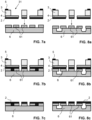
- the remaining sample comprising the nano- or micro-sheet layer 2, the polymer layer 4, the support layer 3 and the spacer elements 5 is transferred to the target substrate 6 ( figure 6a ) and attached to the target substrate 6 ( figure 6b ).
- the support layer 3 and the spacer elements 5 only the nano- or micro-sheet layer 2 remains and forms the final device together with the target substrate 6 ( figure 6c ).
- Figures 7a-c and 8a-c show the transfer of the same sample as in figures 6a-c , but to different target substrates 6.
- the target substrate 6 comprises electrical contacts 61, which in each case form a local elevation on the front surface of the target substrate 6.
- the electrical contacts 61 are contacted and connected by a nano- or micro-sheet element, which is formed by the nano- or micro sheet layer 2.
- the nano- or micro-sheet layer 2 is such applied to the target substrate 6, that it follows the structured front surface of the target substrate 6.
- the nano- or micro-sheet layer 2 not only rests on the local elevations formed by the electrical contacts 61, but also on the bottom of the depressions between the electrical contacts 61. Due to the structuring of the nano- or micro-sheet layer 2, however, some depressions of the target substrate 6 are not covered, meaning that each electrical contacts 61 does not necessarily need to be connected to all other electrical contacts 61.
- Figures 9-15 show other variants of a laminate 14 in addition to the ones of figures 1 and 5 .
- the laminate 14 of figure 9 differs from the one of figure 1 by having and additional insulator layer 7 between the nano- or micro-sheet layer 2 and the polymer layer 4.
- the insulator layer 7 provides electrical insulation.
- the variant of figure 10 differs from the one of figure 9 by the structuring of the polymer layer 4 corresponding to the pattern 31 of the support layer 3. As a consequence, the bottoms of the depressions 311 of the pattern 31 is formed by the insulator layer 7 in each case.
- the insulator layer 7 and the nano- or micro-sheet layer 2 are also structured.
- Figure 12 shows a variant with an insulator layer 7 being arranged between the nano- or micro-sheet layer 2 and the polymer layer 4.
- the insulator layer 7 here extends into the through-going apertures formed by the nano- or micro-sheet layer 2 in such a way that the apertures are completely filled out by the insulator layer 7.
- Figure 1 shows the same laminate 14 as figure 1 , but with an additional structuring of the nano- or micro-sheet layer 2 and of the polymer layer 4 in accordance with the pattern 31 of the support layer 3. Due to this structuring, the bottoms of the depressions 311 are formed by the exposed front surface of the growth substrate 1.
- the variant of figure 14 corresponds to the one of figure 13 with the exception that here the nano- or micro-sheet layer 2 has a uniform thickness, i.e. no structure with depressions or elevations.
- the variant of the laminate 14 shown in figure 15 differs from the one of figure 5 by having an additional insulator layer 7.
- the insulator layer 7 has the same structure with elevations and depressions as the nano- or micro-sheet layer 2 and the polymer layer 4.
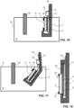
- Figures 16 and 17 show the electrochemical delamination process by means of electrolysis according to two variants.
- the laminate 14 is placed on edge and clamped in an essentially L-shaped sample holder 11 and immersed, together with the sample holder 11, in an electrolyte 9 contained in a beaker 8 (see figure 16 ).
- a clamp 12 attached to the sample holder 11 is used.
- the nano- or micro-sheet layer 2 and the further layers 3 and 4 are only present on some, but not all surface parts of the growth substrate 1.
- an anode 10 is additionally immersed in the electrolyte 9 and an electric voltage is applies between the anode 10 and the metallic growth substrate 1.
- the growth substrate 1 forms the cathode in the electrolysis.
- a connector line 13 serves to apply the electric voltage to the growth substrate 1.
- the sample holder 11 of figure 17 differs from the one of figure 16 by a bend in the holding part.
- the shape of the growth substrate 1 is adapted accordingly.
- the laminate 14 is held in an inclined position by the sample holder 11 during the electrolysis.
- the respective support layer 3 comprises a pattern 31, which is not shown, however, for illustrative reasons.
- Figure 18 shows a further possible design of a sample holder 11.
- the growth substrate 1 is here clamped in both regions above and below the support layer 3.
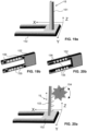
- Figure 19a shows a first version of a pickup element in the form of a forklift 15 used for transferring the nano- or micro-sheet layer 1 together with the support layer 3 and, if present, with the polymer layer 4 after delamination from the growth substrate 1 to the target substrate 6.
- the forklift 15 comprises a fork element 152, which is C-shaped and extends in a horizontal direction.
- a vertically extending support bar 151 is attached to the fork element 152, which serves to hold and move the fork element 152 along all three directions X, Y and Z in space.
- the support bar 151 is attached with its upper end to a respective handling device, such as e.g. a robot arm, not shown in the figure.
- the fork element 152 serves to contact, pick-up, transfer and place a sample comprising the nano- or micro-sheet layer 2 together with the support layer 3 and, if present, the polymer layer 4 after delamination.
- the fork element 152 can be moved underneath or on top of the sample and then lifted, in order to carry the sample on the upper side of the fork element 152.
- the air suction elements 155 and/or the electromagnetic elements 156 can be activated, in order to attract and hold the sample.
- the air suction elements 155 and/or the electromagnetic elements 156 are deactivated again.
- the sample comprises ferromagnetic parts, for example in the form of ferromagnetic pickup elements attached e.g. to the upper side of the support layer 3.
- a second version of a forklift 15 is shown in figures 20a and 20b .
- the fork element 152 is here attached to a vertically extending gear rack 153 that is engaged by a gearwheel 154.
- the gear wheel 154 By rotating the gear wheel 154, which can be a part of a respective motorized handling device, the forklift 15 can be moved along the vertically extending Z-direction.
- a plurality of air suction elements 155 as well as an electromagnetic element 156 in the form of a C-shaped magnetic strip are provided at the underside of the fork element 152.
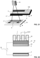
- Figure 21 shows the step of aligning the sample comprising the nano- or micro-sheet layer 2 correctly with the target substrate 6 by means of an image recognition and alignment system 16.
- the image recognition and alignment system 16 comprises a camera, e.g. a CCD-camera, that captures the top surface of the target substrate 6 as well as the position and orientation of the forklift element 152 with the nano- or micro-sheet layer 2 and the support layer 3.
- the fork element 152 is moved such by a controller that the nano- or micro-sheet layer 2 is aligned correctly and placed on the target substrate 6.
- the target substrate 6 can be positioned on a heat plate 18, which can be heated for this purpose.
- the heat plate 18 or another device holding the target substrate 6 can be moveable as well.
- the heat plate 18 can be rotatable about a vertical axis as it is shown with a double arrow in figure 21 .
- the heat plate 18 could for example be movable along the vertical Z-axis and/or along the X- and/or the Y-axis as well.
- Figure 22 shows a variant of the method step of the electrochemical delamination, which does not use an electrolyte in liquid form. Instead, a polymer electrolyte membrane 20 is used, which is attached to the front surface of the support layer 3.
- the pattern 31 of the support layer 3 is present, but not shown in figure 22 due to illustrative reasons. If the pattern 31 comprises depressions 311 in the form of through-going depressions, the polymer electrolyte membrane 20 can have respective depressions as well.
- an anodic gas diffusion electrode 21 is arranged on the front surface of the electrolyte membrane 20, a anodic gas diffusion electrode 21 is arranged. Towards its upper side, the anodic gas diffusion electrode 21 is attached to a holder 22.
- the holder 22 is made of a soft or rigid material, such as polydimethylsiloxane (PDMS) and has a certain porosity and/or permeability, such that water can pass through the holder 22.
- PDMS polydimethylsiloxane
- the holder 22 has a certain porosity and/or permeability, such that water can pass through the holder 22.
- the water can pass from the environment through the holder 22, and the hydrogen ions generated at the anodic gas diffusion electrode 21 pass through the electrolyte membrane 20.
- the support layer 3 and the nano- or micro sheet layer 2 are shown at a distance from each other in figure 22 . Before, during and after carrying out the actual electrochemical delamination, however, the support layer 3 and the nano- or micro sheet layer 2 are attached to each other.
- a water (H 2 O)-source is provided to the holder 22 and an electric voltage is applied by means of a power supply 19 between the anodic gas diffusion electrode 21 and the growth substrate 1, which is made of copper (Cu) and forms the cathode.
- the voltage difference between anode and cathode causes the water molecules (H 2 O) to split into hydrogen ions (H + ) and oxygen (O).
- oxygen gas is generated at the anode, i.e. at the anodic gas diffusion electrode 21.
- the hydrogen ions pass through the anodic gas diffusion electrode 21 and the polymer electrolyte membrane 20 and the support layer 3 and the nano- or micro sheet layer 2.
- the hydrogen gas is formed at the growth substrate 1 and in particular at the interface between the growth substrate 1 and the nano- or micro-sheet layer 2, the hydrogen gas is formed.
- the generation of such hydrogen gas bubbles causes the growth substrate 1 to separate from the nano- or micro-sheet layer 2, meaning that the laminate 14 is delaminated in a dry manner, wherein the laminate 14 remains under dry conditions and does not require to be immersed in an electrolyte.
- hydrogen gas (H 2 ) as a source at the holder 22 and connecting the anodic gas diffusion electrode 21 and the growth substrate 1 to an electrical load results in the generation of the hydrogen ions at the gas diffusion electrode 21, which diffuse through the polymer membrane 20 and the support layer 3 and the nano- or micro sheet layer 2.
- the hydrogen ions react with oxygen ions to form water, which results in the separation of the nano- or micro sheet layer 2.
- the invention is of course not limited to the preceding presented embodiments and a plurality of modifications is possible.
- the polymer layer 4 could well be omitted in all embodiments.
- Elements disclosed with respect to different embodiments can be exchanged, omitted or added.
- a plurality of further modifications is possible.
Landscapes
- Chemical & Material Sciences (AREA)
- Organic Chemistry (AREA)
- Engineering & Computer Science (AREA)
- Materials Engineering (AREA)
- Chemical Kinetics & Catalysis (AREA)
- Electrochemistry (AREA)
- Metallurgy (AREA)
- Nanotechnology (AREA)
- Inorganic Chemistry (AREA)
- Crystallography & Structural Chemistry (AREA)
- Laminated Bodies (AREA)
- Physical Or Chemical Processes And Apparatus (AREA)
Priority Applications (5)
| Application Number | Priority Date | Filing Date | Title |
|---|---|---|---|
| EP22216615.9A EP4389945A1 (fr) | 2022-12-23 | 2022-12-23 | Procédé de fabrication d'un élément en nano ou microfeuilles à l'aide d'une couche de support à motifs |
| PCT/EP2023/085242 WO2024132659A1 (fr) | 2022-12-23 | 2023-12-12 | Procédé de fabrication d'un élément de nano-feuille ou de micro-feuille à l'aide d'une couche de support à motifs |
| US19/134,840 US20260200741A1 (en) | 2022-12-23 | 2023-12-12 | Method for producing a nano-or micro-sheet element with the help of a patterned support layer |
| EP23820948.0A EP4638839A1 (fr) | 2022-12-23 | 2023-12-12 | Procédé de fabrication d'un élément de nano-feuille ou de micro-feuille à l'aide d'une couche de support à motifs |
| CN202380087659.2A CN120390834A (zh) | 2022-12-23 | 2023-12-12 | 借助图案化承载层制备纳米片元件或微米片元件的方法 |
Applications Claiming Priority (1)
| Application Number | Priority Date | Filing Date | Title |
|---|---|---|---|
| EP22216615.9A EP4389945A1 (fr) | 2022-12-23 | 2022-12-23 | Procédé de fabrication d'un élément en nano ou microfeuilles à l'aide d'une couche de support à motifs |
Publications (1)
| Publication Number | Publication Date |
|---|---|
| EP4389945A1 true EP4389945A1 (fr) | 2024-06-26 |
Family
ID=84602108
Family Applications (2)
| Application Number | Title | Priority Date | Filing Date |
|---|---|---|---|
| EP22216615.9A Withdrawn EP4389945A1 (fr) | 2022-12-23 | 2022-12-23 | Procédé de fabrication d'un élément en nano ou microfeuilles à l'aide d'une couche de support à motifs |
| EP23820948.0A Pending EP4638839A1 (fr) | 2022-12-23 | 2023-12-12 | Procédé de fabrication d'un élément de nano-feuille ou de micro-feuille à l'aide d'une couche de support à motifs |
Family Applications After (1)
| Application Number | Title | Priority Date | Filing Date |
|---|---|---|---|
| EP23820948.0A Pending EP4638839A1 (fr) | 2022-12-23 | 2023-12-12 | Procédé de fabrication d'un élément de nano-feuille ou de micro-feuille à l'aide d'une couche de support à motifs |
Country Status (4)
| Country | Link |
|---|---|
| US (1) | US20260200741A1 (fr) |
| EP (2) | EP4389945A1 (fr) |
| CN (1) | CN120390834A (fr) |
| WO (1) | WO2024132659A1 (fr) |
Citations (17)
| Publication number | Priority date | Publication date | Assignee | Title |
|---|---|---|---|---|
| EP2679540A1 (fr) | 2012-06-29 | 2014-01-01 | Graphenea, S.A. | Procédé de fabrication d'une monocouche de graphène sur substrats isolants |
| US20140130972A1 (en) | 2011-06-09 | 2014-05-15 | Institute Of Metal Research Chinese Academy Of Sciences | Method for Transferring Graphene Nondestructively with Low Cost |
| US20140238873A1 (en) | 2013-02-27 | 2014-08-28 | Xuesong Li | Modified bubbling transfer method for graphene delamination |
| US20150068684A1 (en) | 2009-10-16 | 2015-03-12 | Graphene Square Inc. | Roll-to-roll transfer method of graphene, graphene roll produced by the method, and roll-to-roll transfer equipment for graphene |
| US20150240038A1 (en) * | 2014-02-26 | 2015-08-27 | National University Of Singapore | Method and apparatus for transferring graphene to a polymeric substrate |
| EP2937313A1 (fr) | 2014-04-24 | 2015-10-28 | Graphenea, S.A. | Équipement et procédé pour transférer automatiquement un graphène mono-couche à un substrat |
| US20160304352A1 (en) * | 2013-12-05 | 2016-10-20 | National University Of Singapore | Graphene tape |
| EP3135631A1 (fr) | 2015-08-24 | 2017-03-01 | Graphenea, S.A. | Procédé de transfert de graphène |
| WO2017158235A1 (fr) * | 2016-03-15 | 2017-09-21 | Aalto University Foundation | Film composite comprenant une couche électroconductrice |
| US20170365477A1 (en) | 2016-06-15 | 2017-12-21 | Nanomedical Diagnostics, Inc. | Providing a temporary protective layer on a graphene sheet |
| US20170361599A1 (en) | 2016-06-15 | 2017-12-21 | Nanomedical Diagnostics, Inc. | Systems and methods for transferring graphene |
| EP2690198B1 (fr) * | 2012-07-27 | 2018-10-03 | Samsung Electronics Co., Ltd | Appareil et procédé de fabrication d'un dispositif de graphène utilisant l'appareil |
| CN110581063A (zh) | 2019-10-22 | 2019-12-17 | 北京石墨烯研究院 | 一种石墨烯晶圆的转移方法 |
| CN111232964A (zh) | 2020-01-19 | 2020-06-05 | 北京石墨烯研究院 | 一种石墨烯晶圆的转移方法、石墨烯晶圆及鼓泡体系 |
| US20200235212A1 (en) | 2018-08-30 | 2020-07-23 | The Institute of Microelectronics of Chinese Academy of Sciences | Graphene electrochemical transfer method assisted by multiple supporting films |
| US20200387073A1 (en) | 2019-06-07 | 2020-12-10 | Korea Advanced Institute Of Science And Technology | Method for Selective Delamination and Transfer of Thin Film Using Liquid Platform |
| WO2022096640A1 (fr) | 2020-11-05 | 2022-05-12 | Graphenea S.A | Capteur comprenant des transistors à base de graphène |
-
2022
- 2022-12-23 EP EP22216615.9A patent/EP4389945A1/fr not_active Withdrawn
-
2023
- 2023-12-12 EP EP23820948.0A patent/EP4638839A1/fr active Pending
- 2023-12-12 CN CN202380087659.2A patent/CN120390834A/zh active Pending
- 2023-12-12 US US19/134,840 patent/US20260200741A1/en active Pending
- 2023-12-12 WO PCT/EP2023/085242 patent/WO2024132659A1/fr not_active Ceased
Patent Citations (17)
| Publication number | Priority date | Publication date | Assignee | Title |
|---|---|---|---|---|
| US20150068684A1 (en) | 2009-10-16 | 2015-03-12 | Graphene Square Inc. | Roll-to-roll transfer method of graphene, graphene roll produced by the method, and roll-to-roll transfer equipment for graphene |
| US20140130972A1 (en) | 2011-06-09 | 2014-05-15 | Institute Of Metal Research Chinese Academy Of Sciences | Method for Transferring Graphene Nondestructively with Low Cost |
| EP2679540A1 (fr) | 2012-06-29 | 2014-01-01 | Graphenea, S.A. | Procédé de fabrication d'une monocouche de graphène sur substrats isolants |
| EP2690198B1 (fr) * | 2012-07-27 | 2018-10-03 | Samsung Electronics Co., Ltd | Appareil et procédé de fabrication d'un dispositif de graphène utilisant l'appareil |
| US20140238873A1 (en) | 2013-02-27 | 2014-08-28 | Xuesong Li | Modified bubbling transfer method for graphene delamination |
| US20160304352A1 (en) * | 2013-12-05 | 2016-10-20 | National University Of Singapore | Graphene tape |
| US20150240038A1 (en) * | 2014-02-26 | 2015-08-27 | National University Of Singapore | Method and apparatus for transferring graphene to a polymeric substrate |
| EP2937313A1 (fr) | 2014-04-24 | 2015-10-28 | Graphenea, S.A. | Équipement et procédé pour transférer automatiquement un graphène mono-couche à un substrat |
| EP3135631A1 (fr) | 2015-08-24 | 2017-03-01 | Graphenea, S.A. | Procédé de transfert de graphène |
| WO2017158235A1 (fr) * | 2016-03-15 | 2017-09-21 | Aalto University Foundation | Film composite comprenant une couche électroconductrice |
| US20170361599A1 (en) | 2016-06-15 | 2017-12-21 | Nanomedical Diagnostics, Inc. | Systems and methods for transferring graphene |
| US20170365477A1 (en) | 2016-06-15 | 2017-12-21 | Nanomedical Diagnostics, Inc. | Providing a temporary protective layer on a graphene sheet |
| US20200235212A1 (en) | 2018-08-30 | 2020-07-23 | The Institute of Microelectronics of Chinese Academy of Sciences | Graphene electrochemical transfer method assisted by multiple supporting films |
| US20200387073A1 (en) | 2019-06-07 | 2020-12-10 | Korea Advanced Institute Of Science And Technology | Method for Selective Delamination and Transfer of Thin Film Using Liquid Platform |
| CN110581063A (zh) | 2019-10-22 | 2019-12-17 | 北京石墨烯研究院 | 一种石墨烯晶圆的转移方法 |
| CN111232964A (zh) | 2020-01-19 | 2020-06-05 | 北京石墨烯研究院 | 一种石墨烯晶圆的转移方法、石墨烯晶圆及鼓泡体系 |
| WO2022096640A1 (fr) | 2020-11-05 | 2022-05-12 | Graphenea S.A | Capteur comprenant des transistors à base de graphène |
Non-Patent Citations (3)
| Title |
|---|
| MA LAI-PENG ET AL: "Breaking the Rate-Integrity Dilemma in Large-Area Bubbling Transfer of Graphene by Strain Engineering", ADVANCED FUNCTIONAL MATERIALS, vol. 31, no. 36, 23 June 2021 (2021-06-23), DE, pages 2104228, XP093056734, ISSN: 1616-301X, Retrieved from the Internet <URL:https://onlinelibrary.wiley.com/doi/full-xml/10.1002/adfm.202104228> DOI: 10.1002/adfm.202104228 * |
| MA LAI-PENG ET AL: "Supporting Information Breaking the Rate-Integrity Dilemma in Large-Area Bubbling Transfer of Graphene by Strain Engineering", ADVANCED FUNCTIONAL MATERIALS, vol. 31, no. 36, 23 June 2021 (2021-06-23), DE, pages 2104228, XP093057310, ISSN: 1616-301X, Retrieved from the Internet <URL:https://onlinelibrary.wiley.com/doi/full-xml/10.1002/adfm.202104228> DOI: 10.1002/adfm.202104228 * |
| ROHIT N. KARNIK: "Breakthrough for protons", NATURE, vol. 516, 26 November 2014 (2014-11-26), pages 173 - 175, XP093057302, Retrieved from the Internet <URL:https://www.nature.com/articles/nature14074> DOI: 10.1038/nature14074 * |
Also Published As
| Publication number | Publication date |
|---|---|
| WO2024132659A1 (fr) | 2024-06-27 |
| US20260200741A1 (en) | 2026-07-16 |
| CN120390834A (zh) | 2025-07-29 |
| EP4638839A1 (fr) | 2025-10-29 |
Similar Documents
| Publication | Publication Date | Title |
|---|---|---|
| CN109314099B (zh) | 用于转移石墨烯的系统和方法 | |
| KR102391844B1 (ko) | 그래핀의 제조 및 전사 방법 | |
| EP2715778B1 (fr) | Procédé de transfert de films minces | |
| CN102719877B (zh) | 一种低成本无损转移石墨烯的方法 | |
| Kim et al. | A review on transfer process of two-dimensional materials | |
| US9624597B2 (en) | Methods and apparatuses for delaminating process pieces | |
| US8815707B2 (en) | Environmentally-assisted technique for transferring devices onto non-conventional substrates | |
| TW201039297A (en) | Method for isolating a flexible substrate from a carrier and method for fabricating an electric device | |
| CN105377755A (zh) | 转移石墨烯的电化学方法 | |
| US12119138B2 (en) | Method for manufacturing transparent electrode with low surface roughness | |
| CN116040578B (zh) | 一种乐高式范德华异质结及其制备方法 | |
| KR20230118899A (ko) | 중간 폴리머 전사층 상의 2차원 재료 및 이종 구조및 이의 제조 | |
| CN114180562B (zh) | 一种石墨烯转移方法 | |
| TWI740521B (zh) | 脫層方法及藉以製造薄膜裝置之方法 | |
| CN114486960A (zh) | 一种将二维材料转移至透射电子显微镜格栅的方法 | |
| EP4389944A1 (fr) | Procédé électrochimique de fabrication d'un élément en nano ou microfeuilles à l'aide d'une membrane électrolytique | |
| EP4638839A1 (fr) | Procédé de fabrication d'un élément de nano-feuille ou de micro-feuille à l'aide d'une couche de support à motifs | |
| KR101804819B1 (ko) | 박리 조력층의 전사 과정을 포함하는 플렉시블 정보 표시 소자의 제조 방법 | |
| KR101403254B1 (ko) | 나노 구조체를 구비한 소자의 제조방법 | |
| CN107512714A (zh) | 一种基于电化学自分离的大面积低损伤的石墨烯转移方法 | |
| WO2012116324A9 (fr) | Système et procédé de formation de dispositifs semi-conducteurs | |
| NL2035299B1 (en) | Carrier stack for transferring a two-dimensional, 2D, material to a target substrate, and method for transferring the 2D material to a target substrate | |
| CN112176388B (zh) | 一种电镀夹持装置及利用其制备图案化纳米线的方法 | |
| KR20130107174A (ko) | 나노 구조체를 구비한 소자의 제조방법 |
Legal Events
| Date | Code | Title | Description |
|---|---|---|---|
| PUAI | Public reference made under article 153(3) epc to a published international application that has entered the european phase |
Free format text: ORIGINAL CODE: 0009012 |
|
| STAA | Information on the status of an ep patent application or granted ep patent |
Free format text: STATUS: THE APPLICATION HAS BEEN PUBLISHED |
|
| AK | Designated contracting states |
Kind code of ref document: A1 Designated state(s): AL AT BE BG CH CY CZ DE DK EE ES FI FR GB GR HR HU IE IS IT LI LT LU LV MC ME MK MT NL NO PL PT RO RS SE SI SK SM TR |
|
| STAA | Information on the status of an ep patent application or granted ep patent |
Free format text: STATUS: THE APPLICATION IS DEEMED TO BE WITHDRAWN |
|
| 18D | Application deemed to be withdrawn |
Effective date: 20250103 |