EP4390541A1 - Objekttisch - Google Patents
Objekttisch Download PDFInfo
- Publication number
- EP4390541A1 EP4390541A1 EP22216399.0A EP22216399A EP4390541A1 EP 4390541 A1 EP4390541 A1 EP 4390541A1 EP 22216399 A EP22216399 A EP 22216399A EP 4390541 A1 EP4390541 A1 EP 4390541A1
- Authority
- EP
- European Patent Office
- Prior art keywords
- substrate
- clamp
- burls
- object table
- electrically conductive
- Prior art date
- Legal status (The legal status is an assumption and is not a legal conclusion. Google has not performed a legal analysis and makes no representation as to the accuracy of the status listed.)
- Withdrawn
Links
Images


Classifications
-
- G—PHYSICS
- G03—PHOTOGRAPHY; CINEMATOGRAPHY; ANALOGOUS TECHNIQUES USING WAVES OTHER THAN OPTICAL WAVES; ELECTROGRAPHY; HOLOGRAPHY
- G03F—PHOTOMECHANICAL PRODUCTION OF TEXTURED OR PATTERNED SURFACES, e.g. FOR PRINTING, FOR PROCESSING OF SEMICONDUCTOR DEVICES; MATERIALS THEREFOR; ORIGINALS THEREFOR; APPARATUS SPECIALLY ADAPTED THEREFOR
- G03F7/00—Photomechanical, e.g. photolithographic, production of textured or patterned surfaces, e.g. printing surfaces; Materials therefor, e.g. comprising photoresists; Apparatus specially adapted therefor
- G03F7/70—Microphotolithographic exposure; Apparatus therefor
- G03F7/70691—Handling of masks or workpieces
- G03F7/707—Chucks, e.g. chucking or un-chucking operations or structural details
- G03F7/70708—Chucks, e.g. chucking or un-chucking operations or structural details being electrostatic; Electrostatically deformable vacuum chucks
-
- H—ELECTRICITY
- H10—SEMICONDUCTOR DEVICES; ELECTRIC SOLID-STATE DEVICES NOT OTHERWISE PROVIDED FOR
- H10P—GENERIC PROCESSES OR APPARATUS FOR THE MANUFACTURE OR TREATMENT OF DEVICES COVERED BY CLASS H10
- H10P72/00—Handling or holding of wafers, substrates or devices during manufacture or treatment thereof
- H10P72/70—Handling or holding of wafers, substrates or devices during manufacture or treatment thereof for supporting or gripping
- H10P72/72—Handling or holding of wafers, substrates or devices during manufacture or treatment thereof for supporting or gripping using electrostatic chucks
- H10P72/722—Details of electrostatic chucks
-
- H—ELECTRICITY
- H10—SEMICONDUCTOR DEVICES; ELECTRIC SOLID-STATE DEVICES NOT OTHERWISE PROVIDED FOR
- H10P—GENERIC PROCESSES OR APPARATUS FOR THE MANUFACTURE OR TREATMENT OF DEVICES COVERED BY CLASS H10
- H10P72/00—Handling or holding of wafers, substrates or devices during manufacture or treatment thereof
- H10P72/70—Handling or holding of wafers, substrates or devices during manufacture or treatment thereof for supporting or gripping
- H10P72/76—Handling or holding of wafers, substrates or devices during manufacture or treatment thereof for supporting or gripping using mechanical means, e.g. clamps or pinches
- H10P72/7604—Handling or holding of wafers, substrates or devices during manufacture or treatment thereof for supporting or gripping using mechanical means, e.g. clamps or pinches the wafers being placed on a susceptor, stage or support
- H10P72/7614—Handling or holding of wafers, substrates or devices during manufacture or treatment thereof for supporting or gripping using mechanical means, e.g. clamps or pinches the wafers being placed on a susceptor, stage or support characterised by a plurality of individual support members, e.g. support posts or protrusions
-
- H—ELECTRICITY
- H10—SEMICONDUCTOR DEVICES; ELECTRIC SOLID-STATE DEVICES NOT OTHERWISE PROVIDED FOR
- H10P—GENERIC PROCESSES OR APPARATUS FOR THE MANUFACTURE OR TREATMENT OF DEVICES COVERED BY CLASS H10
- H10P72/00—Handling or holding of wafers, substrates or devices during manufacture or treatment thereof
- H10P72/70—Handling or holding of wafers, substrates or devices during manufacture or treatment thereof for supporting or gripping
- H10P72/76—Handling or holding of wafers, substrates or devices during manufacture or treatment thereof for supporting or gripping using mechanical means, e.g. clamps or pinches
- H10P72/7604—Handling or holding of wafers, substrates or devices during manufacture or treatment thereof for supporting or gripping using mechanical means, e.g. clamps or pinches the wafers being placed on a susceptor, stage or support
- H10P72/7616—Handling or holding of wafers, substrates or devices during manufacture or treatment thereof for supporting or gripping using mechanical means, e.g. clamps or pinches the wafers being placed on a susceptor, stage or support characterised by a coating, a hardness or a material
Definitions
- the present invention relates to an object table for clamping a an object such as a lithographic substrate.
- the object table may form part of a lithographic apparatus or lithographic tool.
- a lithographic apparatus is a machine constructed to apply a desired pattern onto a substrate.
- a lithographic apparatus can be used, for example, in the manufacture of integrated circuits (ICs).
- a lithographic apparatus may, for example, project a pattern at a patterning device (e.g., a mask) onto a layer of radiation-sensitive material (resist) provided on a substrate.
- a patterning device e.g., a mask
- resist radiation-sensitive material
- a lithographic apparatus may use electromagnetic radiation.
- the wavelength of this radiation determines the minimum size of features which can be formed on the substrate.
- a lithographic apparatus which uses extreme ultraviolet (EUV) radiation, having a wavelength within the range 4-20 nm, for example 6.7 nm or 13.5 nm, may be used to form smaller features on a substrate than a lithographic apparatus which uses, for example, radiation with a wavelength of 193 nm.
- EUV extreme ultraviolet
- a substrate which is being patterned by a lithographic apparatus is held on a substrate table.
- the substrate table includes a substrate clamp which is configured to securely hold the substrate on the substrate table whilst the substrate is being patterned, and then to allow the substrate to be removed from the substrate table once patterning has been completed.
- the substrate clamp is an electrical clamp (conventional vacuum clamps cannot be used because the EUV lithographic apparatus uses a vacuum environment).
- a problem which may arise in connection with electrical substrate clamps is that it may be difficult to ensure that the substrate is clamped sufficiently strongly to avoid slipping of the substrate during lithographic patterning, whilst at the same time avoiding excessive friction between the substrate table and the substrate.
- the substrate when the substrate is loaded onto the substrate table, with the clamp is switched off, the substrate should be able to settle on the substrate table and release any stress.
- the substrate table is provided with an array of burls, and the friction between the substrate and the burls should be sufficiently low to allow the substrate to relax to a stress-free state. If the substrate does not relax to a stress-free state, but instead remains stressed, then this may correspond with distortion of the substrate. This distortion may lead to poor quality patterns being formed on the substrate. Thus, low friction when the substrate clamp is switched off is desirable.
- the substrate clamp pulls the substrate onto the burls thereby generating friction between the burls and the substrate.
- This friction should be sufficient that localized heating of the substrate, occurring during exposure of a pattern on the substrate, does not generate an expansive force which is sufficiently large to overcome the friction. In other words, when the substrate is heated during lithographic exposure, slippage of the substrate over the burls should not occur.
- an object table comprising an electrostatic clamp which comprises at least one electrode provided between insulating layers, and a second clamp which comprises an array of electrically connected burls, the burls comprising a layer of resistive material at an object receiving surface of the burls.
- the electrostatic clamp provides initial clamping force which is sufficient to avoid slipping of an object on the object table, and the second clamp provides additional clamping force after the initial clamping force.
- the second clamp may be a Johnsen-Rahbek type clamp.
- the resistive material may be doped diamond.
- the resistive material may be diamond doped with Boron.
- the layer of resistive material may have a resistivity of at least 10 6 Ohm cm.
- the layer of resistive material may have a thickness of at least 100nm.
- the electrostatic clamp may be provided with an array of openings.
- the burls may be formed from electrically conductive material which extends through the openings.
- the burls may be integrally formed with an electrically conductive body, and wherein the electrostatic clamp is fixed to the electrically conductive body.
- the electrically conductive body may be provided with annular recesses which surround the burls.
- the electrically conductive body may comprise flat portions located between the burls, the flat portions receiving the electrostatic clamp.
- Electrically conductive material may be provided on top of the electrostatic clamp, the electrically conductive material extending over the burls and electrically connecting the burls.
- the electrostatic clamp may comprise two electrodes provided between insulating layers, the electrodes being electrically isolated from each other.
- the Johnsen-Rahbek clamp may comprise two electrically conductive parts, the electrically conductive parts being electrically isolated from each other.
- a lithographic apparatus comprising an illumination system and a projection system, and further comprising an object table according to the first aspect of the invention.
- the lithographic apparatus may be a dual stage lithographic apparatus with two (or more) object tables.
- the two object (or more) object tables may be according to the first aspect of the invention.
- a lithographic tool wherein the lithographic tool further comprises an object table according to the first aspect of the invention.
- an object table comprising a first clamp configured to clamp an object using a first clamping mechanism and a second clamp configured to clamp an object using a second clamping mechanism.
- the two different clamping mechanisms may be provide different clamping forces which may be applied at different times (e.g. one clamping force may be applied initially and one clamping force may be provided subsequently - such that both clamping forces are applied after a period of time).
- a lithographic method performed using a dual stage lithographic apparatus comprising placing a substrate on a substrate table comprising an electrostatic clamp and a Johnsen-Rahbek clamp, supplying electrical power to the electrostatic clamp and the Johnsen-Rahbek clamp, moving the substrate table to a measurement system of a dual stage lithographic apparatus then measuring properties of the substrate whilst charge accumulates on the Johnsen-Rahbek clamp, and moving the substrate table to a projection system of the dual stage lithographic apparatus, and using the projection system to project a pattern onto the substrate.
- the electrostatic clamp provides initial clamping force which is sufficient to avoid slipping of the substrate on the substrate table during measurement of the substrate, and the Johnsen-Rahbek clamp provides additional force after the initial clamping force.
- the additional force applied by the Johnsen-Rahbek clamp may inhibit slippage of the substrate during lithographic exposure.
- Figure 1 shows a lithographic system comprising a radiation source SO and a lithographic apparatus LA.
- the radiation source SO is configured to generate an EUV radiation beam B and to supply the EUV radiation beam B to the lithographic apparatus LA.
- the lithographic apparatus LA comprises an illumination system IL, a support structure MT configured to support a patterning device MA (e.g., a mask), a projection system PS, a measurement system MS, and a substrate loading system SL.
- the lithographic system further comprises two substrate tables WT1, WT2 which are configured to support a substrate W. Each substrate table WT1, WT2 may be according to an embodiment of the invention.
- the support structure MT may be according to an embodiment of the invention.
- the substrate clamp may comprise an electrostatic clamp and a Johnsen-Rahbek clamp.
- the illumination system IL is configured to condition the EUV radiation beam B before the EUV radiation beam B is incident upon the patterning device MA.
- the illumination system IL may include a facetted field mirror device 10 and a facetted pupil mirror device 11.
- the faceted field mirror device 10 and faceted pupil mirror device 11 together provide the EUV radiation beam B with a desired cross-sectional shape and a desired intensity distribution.
- the illumination system IL may include other mirrors or devices in addition to, or instead of, the faceted field mirror device 10 and faceted pupil mirror device 11.
- the EUV radiation beam B interacts with the patterning device MA. As a result of this interaction, a patterned EUV radiation beam B' is generated.
- the projection system PS is configured to project the patterned EUV radiation beam B' onto the substrate W.
- the projection system PS may comprise a plurality of mirrors 13, 14 which are configured to project the patterned EUV radiation beam B' onto the substrate W held by the substrate table WT2.
- the projection system PS may apply a reduction factor to the patterned EUV radiation beam B', thus forming an image with features that are smaller than corresponding features on the patterning device MA. For example, a reduction factor of 4 or 8 may be applied.
- the projection system PS is illustrated as having only two mirrors 13, 14 in Figure 1 , the projection system PS may include a different number of mirrors (e.g., six or eight mirrors).
- the substrate W may include previously formed patterns. Where this is the case, the lithographic apparatus LA aligns the image, formed by the patterned EUV radiation beam B', with a pattern previously formed on the substrate W.
- a relative vacuum i.e. a small amount of gas (e.g. hydrogen) at a pressure well below atmospheric pressure, may be provided in the radiation source SO, in the illumination system IL, and/or in the environment of the projection system PS (which may also contain the measurement system MS).
- gas e.g. hydrogen
- the radiation source SO shown in Figure 1 is, for example, of a type which may be referred to as a laser produced plasma (LPP) source.
- a laser system 1 which may, for example, include a CO 2 laser, is arranged to deposit energy via a laser beam 2 into a fuel, such as tin (Sn) which is provided from, e.g., a fuel emitter 3.
- tin is referred to in the following description, any suitable fuel may be used.
- the fuel may, for example, be in liquid form, and may, for example, be a metal or alloy.
- the fuel emitter 3 may comprise a nozzle configured to direct tin, e.g. in the form of droplets, along a trajectory towards a plasma formation region 4.
- the laser beam 2 is incident upon the tin at the plasma formation region 4.
- the deposition of laser energy into the tin creates a tin plasma 7 at the plasma formation region 4.
- Radiation, including EUV radiation, is emitted from the plasma 7 during de-excitation and recombination of electrons with ions of the plasma.
- Collector 5 comprises, for example, a near-normal incidence radiation collector 5 (sometimes referred to more generally as a normal-incidence radiation collector).
- the collector 5 may have a multilayer mirror structure which is arranged to reflect EUV radiation (e.g., EUV radiation having a desired wavelength such as 13.5 nm).
- EUV radiation e.g., EUV radiation having a desired wavelength such as 13.5 nm.
- the collector 5 may have an ellipsoidal configuration, having two focal points. A first one of the focal points may be at the plasma formation region 4, and a second one of the focal points may be at an intermediate focus 6, as discussed below.
- the laser system 1 may be spatially separated from the radiation source SO. Where this is the case, the laser beam 2 may be passed from the laser system 1 to the radiation source SO with the aid of a beam delivery system (not shown) comprising, for example, suitable directing mirrors and/or a beam expander, and/or other optics.
- a beam delivery system (not shown) comprising, for example, suitable directing mirrors and/or a beam expander, and/or other optics.
- the laser system 1, the radiation source SO and the beam delivery system may together be considered to be a radiation system.
- the EUV radiation beam B Radiation that is reflected by the collector 5 forms the EUV radiation beam B.
- the EUV radiation beam B is focused at intermediate focus 6 to form an image at the intermediate focus 6 of the plasma present at the plasma formation region 4.
- the image at the intermediate focus 6 acts as a virtual radiation source for the illumination system IL.
- the radiation source SO is arranged such that the intermediate focus 6 is located at or near to an opening 8 in an enclosing structure 9 of the radiation source SO.
- the measurement system MS of the lithographic apparatus is configured to perform measurements of properties of a substrate W held on a substrate table WT1.
- the measurement system MS comprises an alignment system, which is configured to measure the positions of alignment marks on the substrate with reference to alignment marks on the substrate table WT1.
- the measurement system further comprises a level sensor which is configured to measure the topology of the substrate W. These measured properties are used to ensure accuracy when a pattern is subsequently projected onto the substrate W.
- the lithographic apparatus LA is a dual-stage lithographic apparatus. That is, the lithographic apparatus includes two substrate tables WT1, WT2 and is configured such that a substrate W held on one of the substrate tables WT1 is measured by the measurement system MS simultaneously with a pattern being applied to a substrate W held on the other substrate table WT2.
- the substrate tables WT1 may be referred to as a first substrate table
- the other substrate table WT2 may be referred to as a second substrate table.
- Dual-stage lithographic apparatus advantageously provide higher throughput (i.e. exposure of substrates per hour) than single stage lithographic apparatus (which generally perform measurements simultaneously with exposure of a substrate).
- the substrate table WT1 supporting the measured substrate W is moved to be beneath the projection system PS.
- the exposed substrate W supported by the second substrate table WT2 is moved to the substrate loading system SL.
- the substrate loading system SL includes a substrate handler (not depicted) which is configured to remove the patterned substrate W from the second substrate table WT2, and then load a new substrate to be patterned onto the second substrate table. Once the substrate has been loaded onto the second substrate table WT2, the measurement system MS is used to measure alignment mark positions and the topology of the substrate. Simultaneously, the substrate W held on the first substrate table WT1 is exposed by the lithographic apparatus.
- the above method is repeated many times in order to expose many substrates using the lithographic apparatus.
- Each substrate table WT1, WT2 comprises a substrate clamp according to an embodiment of the invention.
- the substrate clamp is switched off before an exposed substrate is to be removed from the substrate table, thereby allowing a substrate handler of the substrate loading system to easily remove the substrate from the substrate table.
- An unexposed substrate is then placed on the substrate table WT1 (or WT2), following which the substrate clamp is switched on.
- FIG 2 schematically depicts in cross section part of one of the substrate tables WT1 of Figure 1 .
- the other substrate table WT2 may have the same construction.
- the substrate table WT1 comprises a base 20 with a flat lowermost surface 22.
- An array of burls 24 project upwardly from the base 20 (only some are labelled to avoid over-complicating Figure 2 ).
- the base 20 In between the burls 24 the base 20 has a flat upper surface 26 (only one flat area is labelled to avoid over-complicating Figure 2 ).
- An annular recess 28 surrounds each burl 24, thereby providing separation between the burls and the flat upper surface area 26. This separation decreases the stiffness of the burls, making the burls more flexible. This in turn reduces a likelihood of thermal slip of a substrate on the burls (the burls can bend to accommodate some expansion of the substrate during exposure of the substrate).
- the base 20 and burls 24 may be integrally formed from the same material.
- the material used to form the base 20 and the burls 24 is an electrical conductor, and may be silicon carbide, or some other conductive ceramic.
- the burls 24 are electrically connected via the base 20.
- a layer of resistive material 30 is provided on the tip of each burl 24.
- the resistive material may for example be diamond which has been doped with Boron. Other dopants may be used.
- the dopant should increase the conductivity of the diamond (or other resistive material 30).
- the dopant may be provided at a concentration which provides the diamond (or other resistive material) with a resistivity between 10 13 Ohm cm and 10 6 Ohm cm.
- the dopant may be provided at a concentration which provides the diamond (or other resistive material) with a resistivity of around 10 8 Ohm cm.
- the base 20 of the substrate table WT1 is connected to a source of electrical current (not depicted).
- the source of electrical current is controlled by a controller (not depicted) which is configured to connect and disconnect the current source from the base 20 (and may apply a desired voltage to the base).
- the current source may be connected to the base 20 on such that current is supplied to the base (and a voltage is applied to the base).
- the base 20 is a conductor, charge may flow through the base easily. Due to a voltage difference between the substrate W and the base 20, some current will flow through the resistive layer 30 on each burl 24. As a result, charge may accumulate on the upper surface of each resistive layer 30. This charge will give rise to the Johnsen-Rahbek clamping effect, thereby clamping the substrate to the substrate table WT1.
- the base 20, burls 24 and resistive layers 30 form a Johnsen-Rahbek clamp 32.
- the substrate table WT1 further comprises an electrostatic clamp 40.
- the electrostatic clamp comprises an electrode 41 which is sandwiched between two layers of dielectric 42.
- the electrode 41 and dielectric 42 include openings 44 through which the burls 24 project.
- the dielectric may for example be glass, sapphire or silica.
- the electrode may for example be formed from chromium, aluminium or any coated metal layer.
- the electrostatic clamp 40 may be secured to the base 20 by adhesive 46.
- the substrate table WT1 thus comprises a Johnsen-Rahbek clamp 32 and an electrostatic clamp 40.
- the substrate table WT1 may include further layers, such as a support layer (not depicted).
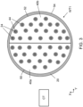
- Figure 3 schematically depicts the substrate table WT1 viewed from above.
- the substrate table WT1 comprises the base 20 and first and second parts 40a,b of the electrostatic clamp.
- a first half 40a of the electrostatic clamp is generally semi-circular.
- Openings 44 through which burls 24 project may be seen.
- the openings and the burls are schematically depicted, and in practice there may be many more burls than depicted, with the burls (and openings) being significantly smaller than schematically depicted.
- the burls may have a diameter at an upper end of around 200 microns.
- the openings may have a diameter of around 600 microns.
- the burls may be separated by around 1.5mm.
- the substrate table WT1 may have a diameter of around 300 mm. These are merely example dimensions, and other dimensions may be used.
- a voltage source 50 is connected to the first half 40a of the electrostatic clamp 40, and is configured to apply a voltage to the first half of the electrostatic clamp.
- the second half of the electrostatic clamp 40b is also semi-circular, and is located adjacent to, but not in electrical contact with, the first half of the electrostatic clamp.
- a voltage source 52 is connected to the second half of the electrostatic clamp 40b and is configured to apply a voltage to the electrostatic clamp.
- the voltage sources 50, 52 may be configured to apply voltages of opposite polarities to the two halves 40a, 40b of the electrostatic clamp. This is desirable because it may avoid or reduce a general build-up of electrostatic charge on a substrate which is being supported by the substrate table WT1.
- a source of electrical current 54 is connected to the base 20.
- the current source 54 may be an amplifier that controls both current and voltage.
- the voltage and current sources 50, 52, 54 may all be controlled by a controller CT. Although the electrical sources 50, 52, 54 and the controller CT are depicted as being separate from the substrate table WT1, in practice they may all be located within the substrate table.
- the Johnsen-Rahbek clamp 21 and the electrostatic clamp 40 are electrically isolated from each other. Specifically, the electrode 41 of the electrostatic clamp 40 does not contact the base 20 or the burls 24 (as may be seen from Figure 2 ). This allows the electrostatic clamp 40 and the Johnsen-Rahbek clamp 32 to be operated independently of each other.
- a substrate W is loaded onto the first substrate table WT1.
- the electrostatic clamp 40 is switched on and clamps the substrate to the first substrate table WT1. Clamping force is applied by the electrostatic clamp 40 instantaneously.
- the Johnsen-Rahbek clamp 32 is also switched on. However, unlike the electrostatic clamp 40, the Johnsen-Rahbek clamp 32 takes a significant time to establish a clamping force which is applied to the substrate.
- the voltage which is applied to the first and second parts 40a, 40b is applied effectively instantaneously and thus clamps the substrate immediately when voltage sources 50, 52 are connected to the electrodes 40a, 40b.
- the significant time before clamping force is applied by the Johnsen-Rahbek clamp is not problematic, because the substrate W supported by the first substrate table WT1 is not exposed immediately after the substrate is placed on the substrate table. Instead, as explained further above, properties of the substrate W are measured by the measurement system MS. This measurement by the measurement system MS takes some time, typically several seconds, and this provides sufficient time for the Johnsen-Rahbek clamping force to be fully established. In an example, the Johnsen-Rahbek force may be fully established within around 1 second.
- the electrostatic clamp provides initial clamping force which is sufficient to avoid slipping of the substrate W on the first substrate table WT1 during measurement of the substrate.
- the first substrate table WT1 is moved to be beneath the projection system PS.
- the second substrate table WT2 is moved to the substrate loading system SL.
- Lithographic exposure of the substrate W on the first substrate table WT1 commences.
- the Johnsen-Rahbek force has been fully established by the Johnsen-Rahbek clamp 32.
- the first substrate table WT1 passes back from beneath the projection system PS to the substrate loading system SL.
- the Johnsen-Rahbek clamp 32 may be switched off (i.e. the current source 54, which may be an amplifier that controls current and voltage, may be set to 0V), as a result of which charge will migrate back through the resistive layers 30 and dissipate within the base 20.
- the electrostatic clamp 40 may be switched off (e.g. set to 0V) when the substrate table WT1 has arrived at the substrate loading system SL.
- the charge at the upper surfaces of the resistive layers 30 may have dissipated sufficiently once the substrate table has arrived at the substrate loading system SL such that the substrate W may be lifted from the substrate table WT1 by a substrate handler. That is, the substrate W is no longer clamped to the substrate table WT1.
- the voltage sources 50, 52 and the current source 54 may all be set to 0V.
- doped diamond as the resistive layer 30 is particularly advantageous. This is because diamond has material properties (which may be referred to as tribology) which are desirable for a substrate table WT1. In particular, diamond is extremely hard wearing, and thus is not abraded over time by substrates. This is advantageous because abrasion of a surface will generate particulate contamination, and particulate contamination is not desirable in a lithographic apparatus.
- the resistivity of the doped diamond resistive layer 30 may be selected as desired via the amount of doping which is provided in the diamond.
- the dopant may be Boron.
- Using a dopant to obtain a desired resistance advantageously does not have a significant effect upon the tribology of the diamond (the tribology is determined by the diamond). This is because the percentage of the dopants is very small compared to the carbon atoms percentage. The tribology is determined by the crystal structure of the diamond, and the dopant does not have a significant effect on this.
- the resistive layer 30 It may be desirable to have a resistance which is sufficiently high that a high leakage current through the resistive layer 30 is avoided. This is because a high leakage current could undesirably cause significant heating of the substrate and/or could damage the substrate (e.g. if the substrate had a conductive lowermost surface). Conversely, since the Johnsen-Rahbek clamping force arises from charge accumulation at the upper surface of the resistive layer 30, it may be desirable that the resistance of the resistive layer is not so high that it takes too long for current to accumulate on the upper surface of the resistive layer and provide clamping force.
- the doped resistive layer 30 may for example have a resistivity between 10 13 Ohm cm and 10 6 Ohm cm.
- the doped resistive layer 30 may for example have a resistivity of around 10 8 Ohm cm.
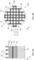
- Figure 4 schematically depicts a substrate table WT1 comprising a substrate clamp according to an alternative embodiment of the invention.
- Figure 4A schematically depicts part of the substrate clamp in cross-section
- Figure 4B schematically depicts the substrate clamp viewed from above.
- the substrate clamp comprises a layer of ceramic such as SiSiC 60.
- a layer of dielectric 62 is provided on top of the ceramic layer 60 .
- the dielectric may for example be glass, or any other insulator.
- An electrode 64 is located on top of the dielectric layer 62.
- a further dielectric layer 66 which may also be glass or any other insulator, is provided on top of the electrode 64.
- the dielectric layer 66 includes burls 68 provided in an array (as with the embodiment depicted in Figures 2 and 3 ).
- two electrodes 64a,b are labelled, separated by a dashed line, although the electrodes are beneath the further dielectric layer 66 and so are not visible.
- Electrically conductive material 70 e.g. CrN is deposited onto the further dielectric layer 66 (which may be referred to as the upper dielectric layer 66) in a grid-like arrangement.
- the electrically conductive material 70 extends between the burls 68 and passes over tops of the burls. The burls are thus electrically connected by the electrically conductive material 70.
- the electrically conductive material may for example have a thickness of between 100nm and 10 microns.
- a resistive layer 72 is provided on top of the electrically conductive material 70 on each burl 68.
- the resistive layer 72 may be formed for example from diamond which has been doped, e.g. with Boron.
- the resistive layer 72 may for example have a thickness of between 100nm and 10 microns.
- the concentration of the dopant may be selected to provide the resistive layers 72 with a desired resistance.
- the resistive layer 72 may for example have a resistivity between 10 13 Ohm cm and 10 6 Ohm cm.
- the resistive layer 72 may for example have a resistivity of around 10 8 Ohm cm.
- the substrate clamp may include additional layers beneath the ceramic layer 60.
- the structure depicted in Figure 4 may be made two times, one of the structures being inverted and then bonded to the other structure.
- the lowermost resistive material which provides Johnsen-Rahbek clamping may be omitted from the lowermost structure.
- the lowermost electrically conductive material may be retained.
- the substrate table WT1 may include further layers, such as a support layer (not depicted).
- Two voltage sources 84, 86 are connected to the first and second electrodes 64a,b.
- a current source 88 is connected to the electrically conductive material 70.
- the current source 88 may be an amplifier that controls both current and voltage.
- a controller CT controls operation of the voltage and current sources 84, 86, 88. These may be located within the substrate table WT1.
- the first and second electrodes 64a,b form an electrostatic clamp.
- the electrically conductive material 70 and resistive layers 72 form a Johnsen-Rahbek clamp.
- the substrate table WT1 thus comprises a Johnsen-Rahbek clamp and an electrostatic clamp.
- the base of the Johnsen-Rahbek clamp has been described and depicted in Figure 3 as being a single entity to which a single current is applied.
- the electrically conductive material 70 is interconnected to form a single conductor to which a single current is applied.
- the Johnsen-Rahbek clamp may be provided as two or more electrically isolated entities.
- the two or more electrically isolated parts of the base may be structurally connected to form a rigid support for the substrate.
- the arrangement of the parts of the Johnsen-Rahbek clamp may for example be two semicircles, in a manner which corresponds with that depicted in Figure 3 for the electrostatic clamp. Other configurations of two parts of the Johnsen-Rahbek clamp may be provided.
- gaps may be provided between the conductive material along a central line of the clamp.
- gaps may be provided where the dashed line is shown in Figure 4B .
- Other configurations of two or more parts of the Johnsen-Rahbek clamp may be provided.
- the number of burls in each half of the Johnsen-Rahbek clamp are the same.
- the Johnsen-Rahbek clamp and the electrostatic clamp may have different arrangements. For example, a separation between two halves of the electrostatic clamp may extend in the Y-direction and separation between two halves of the Johnsen-Rahbek clamp may extend in the X-direction (Cartesian coordinates are included in the Figures for ease of description and understanding).
- the Johnsen-Rahbek clamp is provided in two parts, these parts may be provided with opposite polarities in order to minimise charge accumulation over time. Where this is the case, it may be desirable to provide the resistive layer 30, 72 with sufficient resistance to avoid substantial current flow between oppositely charged parts of the Johnsen-Rahbek clamp (i.e. via the substrate).
- the resistivity of the resistive layers 30, 72 may be at least 10 6 Ohm cm.
- the resistivity of the resistive layers 30, 72 may be up to 10 13 Ohm cm.
- the resistivity of the resistive layers 30, 72 may for example be around 10 8 Ohm cm.
- the voltage source may be disconnected from the Johnsen-Rahbek clamp before exposure of the substrate W has been completed. This may be done if sufficient time is not available after exposure of the substrate has been completed to allow the Johnsen-Rahbek force to be sufficiently reduced such that the substrate can be removed from the substrate table.
- a substrate may be removed from a substrate table WT1, WT2 as soon as the substrate table has arrived at the substrate loading system, and once the substrate has been removed a new substrate for exposure may be immediately placed upon the substrate table.
- measurement of properties of the newly loaded substrate may be completed before exposure of a substrate is completed. As a result, there may be a pause during which the measured substrate is no longer being measured but instead is merely waiting until exposure of the substrate being exposed has been completed, so that the measured substrate can at that time be moved to be beneath the projection system PS of the lithographic apparatus.
- this pause may be instead imposed at the point in time when the substrate table arrives at the substrate loading system SL for unloading. That is, available time which would otherwise not be used during measurement of the substrate may be used to allow further discharge of the Johnsen-Rahbek clamp before the substrate is removed from the substrate table.
- the pause may for example be 1 second or less.
- Embodiments of the invention may provide clamping force at the burls arising from the Johnsen-Rahbek effect and may in addition provide electrostatic clamping at areas which are between the burls.
- clamping force may be applied across substantially an entire substrate which is held on the substrate table WT1, WT2.
- embodiments of the invention have been described in connection with a substrate and substrate tables, in other embodiments the invention may be used to clamp a mask MA (or other patterning device) to a support structure MT of a lithographic apparatus (see Figure 1 ), or to clamp some other object. In general, embodiments of the invention may be used to clamp an object.
- the table of embodiments of the invention may be referred to as an object table.
- a voltage of around 3kV may be applied to the conductor(s) of the electrostatic clamp.
- a voltage of less than 250V may be applied to the Johnsen-Rahbek clamp.
- the voltage applied to the Johnsen-Rahbek clamp may be less than 10V, e.g. as little as 3V.
- Embodiments of the invention generally relate to a combination of an electrostatic clamp, and a clamp with an array of electrically connected burls, the burls comprising a layer of resistive material at an object receiving surface of the burls.
- embodiments of the invention relate to an object table comprising two clamps which use different clamping mechanisms.
- the first clamping mechanism may be electrostatic with the second clamping mechanism being Johnsen-Rahbek type clamping.
- the first clamping mechanism may be vacuum with the second clamping mechanism being electrostatic.
- Other combinations of clamping mechanism may be used.
- lithographic apparatus in the manufacture of ICs, it should be understood that the lithographic apparatus described herein may have other applications. Possible other applications include the manufacture of integrated optical systems, guidance and detection patterns for magnetic domain memories, flat-panel displays, liquid-crystal displays (LCDs), thin-film magnetic heads, etc.
- Embodiments of the invention may form part of a mask inspection apparatus, a metrology apparatus, or any apparatus that measures or processes an object such as a wafer (or other substrate) or mask (or other patterning device). These apparatuses may be generally referred to as lithographic tools. Such a lithographic tool may use vacuum conditions or ambient (non-vacuum) conditions.
- a substrate clamp according to an embodiment of the invention may form part of a lithographic tool.
Landscapes
- Physics & Mathematics (AREA)
- General Physics & Mathematics (AREA)
- Exposure And Positioning Against Photoresist Photosensitive Materials (AREA)
- Container, Conveyance, Adherence, Positioning, Of Wafer (AREA)
- Electron Beam Exposure (AREA)
Priority Applications (4)
| Application Number | Priority Date | Filing Date | Title |
|---|---|---|---|
| EP22216399.0A EP4390541A1 (de) | 2022-12-23 | 2022-12-23 | Objekttisch |
| CN202380087703.XA CN120390982A (zh) | 2022-12-23 | 2023-11-16 | 载物台 |
| PCT/EP2023/082029 WO2024132310A1 (en) | 2022-12-23 | 2023-11-16 | Object table |
| TW112148054A TW202441288A (zh) | 2022-12-23 | 2023-12-11 | 物件台 |
Applications Claiming Priority (1)
| Application Number | Priority Date | Filing Date | Title |
|---|---|---|---|
| EP22216399.0A EP4390541A1 (de) | 2022-12-23 | 2022-12-23 | Objekttisch |
Publications (1)
| Publication Number | Publication Date |
|---|---|
| EP4390541A1 true EP4390541A1 (de) | 2024-06-26 |
Family
ID=84602102
Family Applications (1)
| Application Number | Title | Priority Date | Filing Date |
|---|---|---|---|
| EP22216399.0A Withdrawn EP4390541A1 (de) | 2022-12-23 | 2022-12-23 | Objekttisch |
Country Status (4)
| Country | Link |
|---|---|
| EP (1) | EP4390541A1 (de) |
| CN (1) | CN120390982A (de) |
| TW (1) | TW202441288A (de) |
| WO (1) | WO2024132310A1 (de) |
Citations (4)
| Publication number | Priority date | Publication date | Assignee | Title |
|---|---|---|---|---|
| US20040114124A1 (en) * | 2002-08-23 | 2004-06-17 | Asml Netherlands B.V. | Chuck, lithographic apparatus and device manufacturing method |
| US20110164343A1 (en) * | 2010-01-05 | 2011-07-07 | Michael Sogard | Hybrid electrostatic chuck |
| JP2013251353A (ja) * | 2012-05-31 | 2013-12-12 | Kyocera Corp | 静電チャック、吸着方法及び吸着装置 |
| WO2021250074A1 (en) * | 2020-06-11 | 2021-12-16 | Asml Netherlands B.V. | Object holder, electrostatic sheet and method for making an electrostatic sheet |
-
2022
- 2022-12-23 EP EP22216399.0A patent/EP4390541A1/de not_active Withdrawn
-
2023
- 2023-11-16 WO PCT/EP2023/082029 patent/WO2024132310A1/en not_active Ceased
- 2023-11-16 CN CN202380087703.XA patent/CN120390982A/zh active Pending
- 2023-12-11 TW TW112148054A patent/TW202441288A/zh unknown
Patent Citations (4)
| Publication number | Priority date | Publication date | Assignee | Title |
|---|---|---|---|---|
| US20040114124A1 (en) * | 2002-08-23 | 2004-06-17 | Asml Netherlands B.V. | Chuck, lithographic apparatus and device manufacturing method |
| US20110164343A1 (en) * | 2010-01-05 | 2011-07-07 | Michael Sogard | Hybrid electrostatic chuck |
| JP2013251353A (ja) * | 2012-05-31 | 2013-12-12 | Kyocera Corp | 静電チャック、吸着方法及び吸着装置 |
| WO2021250074A1 (en) * | 2020-06-11 | 2021-12-16 | Asml Netherlands B.V. | Object holder, electrostatic sheet and method for making an electrostatic sheet |
Also Published As
| Publication number | Publication date |
|---|---|
| CN120390982A (zh) | 2025-07-29 |
| WO2024132310A1 (en) | 2024-06-27 |
| TW202441288A (zh) | 2024-10-16 |
Similar Documents
| Publication | Publication Date | Title |
|---|---|---|
| TWI446482B (zh) | 靜電鉗微影裝置及製造靜電鉗之方法 | |
| CN105103052B (zh) | 物体保持装置及制造物体保持装置的方法 | |
| US12235592B2 (en) | Object holder, electrostatic sheet and method for making an electrostatic sheet | |
| US12197139B2 (en) | Object holder, tool and method of manufacturing an object holder | |
| JP5920223B2 (ja) | ハイブリッド静電チャック | |
| CN118511129A (zh) | 物体保持器、包括这种物体保持器的光刻设备、以及用于物体保持器的方法 | |
| JP3930038B2 (ja) | マスクをアースに電気的に接続するためのシステム、マスク | |
| EP4390541A1 (de) | Objekttisch | |
| KR20250133333A (ko) | 물체 홀더 | |
| EP4488761A1 (de) | Elektrostatische klemmvorrichtung | |
| EP4379783A1 (de) | Elektrostatische klemme, greiferanordnung mit dieser klemme, lithographisches system mit einer elektrostatischen klemme und verfahren zur herstellung einer elektrostatischen klemme | |
| WO2025008135A1 (en) | Electrostatic clamp arrangement | |
| WO2025201980A1 (en) | Electrostatic clamp |
Legal Events
| Date | Code | Title | Description |
|---|---|---|---|
| PUAI | Public reference made under article 153(3) epc to a published international application that has entered the european phase |
Free format text: ORIGINAL CODE: 0009012 |
|
| STAA | Information on the status of an ep patent application or granted ep patent |
Free format text: STATUS: THE APPLICATION HAS BEEN PUBLISHED |
|
| AK | Designated contracting states |
Kind code of ref document: A1 Designated state(s): AL AT BE BG CH CY CZ DE DK EE ES FI FR GB GR HR HU IE IS IT LI LT LU LV MC ME MK MT NL NO PL PT RO RS SE SI SK SM TR |
|
| STAA | Information on the status of an ep patent application or granted ep patent |
Free format text: STATUS: THE APPLICATION IS DEEMED TO BE WITHDRAWN |
|
| 18D | Application deemed to be withdrawn |
Effective date: 20250103 |