EP4390575A1 - System zur einstellung einer beleuchtungsfunktion einer uhr - Google Patents
System zur einstellung einer beleuchtungsfunktion einer uhr Download PDFInfo
- Publication number
- EP4390575A1 EP4390575A1 EP22215940.2A EP22215940A EP4390575A1 EP 4390575 A1 EP4390575 A1 EP 4390575A1 EP 22215940 A EP22215940 A EP 22215940A EP 4390575 A1 EP4390575 A1 EP 4390575A1
- Authority
- EP
- European Patent Office
- Prior art keywords
- covering element
- illumination
- light source
- layer
- une
- Prior art date
- Legal status (The legal status is an assumption and is not a legal conclusion. Google has not performed a legal analysis and makes no representation as to the accuracy of the status listed.)
- Pending
Links
Images


Classifications
-
- G—PHYSICS
- G04—HOROLOGY
- G04B—MECHANICALLY-DRIVEN CLOCKS OR WATCHES; MECHANICAL PARTS OF CLOCKS OR WATCHES IN GENERAL; TIME PIECES USING THE POSITION OF THE SUN, MOON OR STARS
- G04B19/00—Indicating the time by visual means
- G04B19/30—Illumination of dials or hands
-
- G—PHYSICS
- G04—HOROLOGY
- G04B—MECHANICALLY-DRIVEN CLOCKS OR WATCHES; MECHANICAL PARTS OF CLOCKS OR WATCHES IN GENERAL; TIME PIECES USING THE POSITION OF THE SUN, MOON OR STARS
- G04B45/00—Time pieces of which the indicating means or cases provoke special effects, e.g. aesthetic effects
- G04B45/0015—Light-, colour-, line- or spot-effects caused by or on stationary parts
-
- G—PHYSICS
- G04—HOROLOGY
- G04G—ELECTRONIC TIME-PIECES
- G04G17/00—Structural details; Housings
- G04G17/02—Component assemblies
-
- G—PHYSICS
- G04—HOROLOGY
- G04G—ELECTRONIC TIME-PIECES
- G04G19/00—Electric power supply circuits specially adapted for use in electronic time-pieces
-
- G—PHYSICS
- G04—HOROLOGY
- G04G—ELECTRONIC TIME-PIECES
- G04G19/00—Electric power supply circuits specially adapted for use in electronic time-pieces
- G04G19/10—Arrangements for supplying back-up power
-
- G—PHYSICS
- G04—HOROLOGY
- G04G—ELECTRONIC TIME-PIECES
- G04G21/00—Input or output devices integrated in time-pieces
- G04G21/04—Input or output devices integrated in time-pieces using radio waves
-
- G—PHYSICS
- G04—HOROLOGY
- G04G—ELECTRONIC TIME-PIECES
- G04G21/00—Input or output devices integrated in time-pieces
- G04G21/08—Touch switches specially adapted for time-pieces
-
- G—PHYSICS
- G04—HOROLOGY
- G04G—ELECTRONIC TIME-PIECES
- G04G9/00—Visual time or date indication means
- G04G9/0023—Visual time or date indication means by light valves in general
- G04G9/0029—Details
- G04G9/0035—Details constructional
- G04G9/0041—Illumination devices
Definitions
- the invention relates to a system for controlling/adjusting an illumination function of a watch comprising at least one trim element provided with an autonomous lighting device.
- Such systems generally include a push button which is associated with this light source. Activation of the push button to turn the light source on or off on demand
- the invention aims to overcome these drawbacks by proposing a system for controlling/adjusting an illumination function of a watch which is easy to use, robust and reliable.
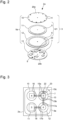
- FIG. 1 On the figure 1 is illustrated a system 100 for controlling/adjusting an illumination/lighting function of a watch comprising at least one trim element provided with an autonomous lighting device.
- Such an illumination function of this watch can be configured in particular from a portable electronic device 110 or mobile of this system 100.
- Such an electronic device 110 makes it possible to ensure the adjustment of this function by transmitting , as we will see in the following, suitable instructions for a control unit of the autonomous lighting device arranged in said at least one covering element of this watch.
- Such an adjustment of this function makes it possible to vary the characteristics of this illumination of the trim element of the watch according to the will/wish of the user of this watch in order to create functional, aesthetic and /or surprising playful, in contrast with unlit parts of this covering element.
- illumination of this covering element can have a more or less diffuse, discreet, soft and pleasant appearance, these characteristics being able to be varied practically infinitely depending on the desired aesthetic rendering, which increases the aesthetic quality. final of the watch.
- Such a system 100 therefore comprises the portable electronic device as well as said watch, the two being capable of carrying out data exchanges between them by implementing for example near field communication technology.
- the watch may for example be an electronic, electromechanical and/or mechanical watch, and in particular a sports watch or a so-called “luxury” watch.
- the covering elements 2a, 2b correspond to all of the constituent parts of the watch surrounding a movement, contributing in particular to its external presentation, to its protection, to its fixing, to its control.
- These trim elements also give this watch its aesthetic and style, and also allow all of its functions to be indicated. More precisely and with reference to figures 1 And 2 , these constituent parts considered here include in a non-exhaustive and non-limiting manner: a back, a middle part 31, a dial 2a, 2b, a bezel 32, a push button, a winding crown and/or a crown cap, etc. ...
- the watch therefore comprises the middle part 31 delimiting with the back and the dial 2a, 2b, an interior volume of a box 30 of this watch. Box 30 is closed on top with a mirror.
- at least one trim element 2a, 2b of this watch 1 comprises an autonomous lighting device 3 provided with at least one light source 4. The light produced by this said at least one light source 4 illuminates in whole or in part the covering element 2a, 2b to be illuminated, namely the dial 2a, 2b in the particular embodiment illustrated on the figures 1 to 5 .
- the watch movement is a mechanical movement.
- this movement can be an electronic movement or even an electromechanical movement.
- the watch movement drives, in a manner known to those skilled in the art, a display comprising an hour hand, a minute hand and possibly a second hand.
- the dial 2a, 2b has a through hole receiving the axis of the hands.
- the covering element here a dial, therefore includes the autonomous lighting device.
- This lighting device 3 includes its own electrical power supply means as we will see later.
- Such a lighting device 3 is said to be autonomous in particular with respect to the movement of the watch 1 and in particular the energy source driving this movement.
- this energy source is generally an electrical power supply as in an electromechanical movement or even an electronic movement. Under these conditions, we understand that the energy used by this lighting device 3 does not come at the expense of the autonomy of such a movement.
- Such a lighting device 3 comprises functional elements such as: said at least one light source 4 also called light source, an independent electrical power supply unit 21, a communication module 22 and a control unit 7.
- the electrical power unit 21 comprises an electrical energy accumulator 6 and a photovoltaic module 5 comprising at least one photovoltaic cell also called solar cell.
- This photovoltaic module 5 is connected to the electrical energy accumulator 6 via connection elements referenced 17b and 18 on the figures 3 And 5 .
- This photovoltaic module 5 may comprise one or more elementary cells of the heterojunction or multijunction type, connected in parallel or in series.
- Each photovoltaic cell of the module can be produced, in a manner known to those skilled in the art, from semiconductor materials based on copper, indium, gallium and selenium, based on cadmium telluride, based on monocrystalline gallium arsenide or based on monocrystalline or polycrystalline silicon, or with perovskites. It should be noted that these examples are non-limiting and that those skilled in the art will be able to find the type of photovoltaic cell suitable for the invention.
- control unit 7 also called microcontroller, comprises an electronic circuit 8 comprising hardware resources in particular at least one processor cooperating with memory elements as well as address, data and control.
- This control unit 7 includes in its memory elements an algorithm for managing the illumination of said at least one light source 4. Such an algorithm is executed by the processor of this control unit 7 taking into account instructions for illuminations received from the portable electronic device and/or data from sensors event included in the lighting device 3 and/or the electronic device 110 in order to ensure management of the operation of said at least one light source 4.
- Such data can for example provide information relating to events detected by these sensors, said events being likely to contribute to the switching on/off of said at least one light source 4.
- These events may include, in a non-limiting manner, and non-exhaustive: the detection of a particular level of brightness in the environment of the watch, the detection of a particular sound element or a particular sound level, the detection of a particular visual object, the detection of a movement carried out by a part of the user's body on which the watch and/or the electronic device is included, the detection of a geographical location of the user of the watch and therefore of the watch, the detection of a notification relating to a function of the electronic device, the detection of a notification relating to an application executed by the electronic device, the detection of reception of a message by the electronic device, etc.
- this control unit 7 is capable of managing/controlling the operation of the light sources 4 simultaneously and/or in sequence.
- each light source 4 is managed/controlled by this control unit separately.
- the management of the operation of each light source 4 can consist in a non-limiting and non-exhaustive manner of switching on and off operations of this source 4.
- Such a control unit 7 can also include in its memory elements an algorithm for managing the electrical energy accumulator 6, in particular the management of its recharging by the photovoltaic module 5 and the management of the electrical consumption by said light source. 4.
- the communication module 22 is preferably wireless, it may be a near field communication module of the NFC type (acronym for “Near Field Communication”) which therefore implements for example short-range and high-frequency wireless communication technologies.
- This communication module 22 can for example operate in the frequency bands relating to high HF frequencies, for example at 13.56 MHz.
- a wireless communication module 22 can be a Bluetooth TM type communication module.
- Such distances can be between approximately 0 and 10 cm, and preferably between 0 and 5 cm.
- the communication module 22 can be of the passive type with energy supplied to it by the radio frequencies emitted by the communication device of the electronic device 110.
- the communication module 7 of the watch 1 can be of the passive type. active type with energy supplied to it by the power supply unit 21 of the lighting device.
- the communication module 22 comprises an electronic chip, at least one antenna and a connector 23 making it possible to connect said module 22 to the control unit 7.
- the chip which is connected to said at least one antenna comprises material elements and software.
- the hardware and/or software elements of the chip comprise at least one microprocessor cooperating with memory elements.
- the portable electronic device 110 also called a user terminal, is a device capable of being worn and transported by a user. This is the case, for example, of a smartphone, a phablet or even a tablet. Naturally, devices requiring mains power, for example desktop computers, are excluded from this definition. Devices 110, such as for example a laptop computer to which a sensor is connected by wireless or wire, are also excluded from this definition.
- This electronic device 110 comprises a housing 27 in which an electronic circuit 26 is arranged.
- This electronic circuit 26 comprises a controller 24 and a communication unit 25, in particular an NFC type near field communication unit 25, both powered by a battery.
- This controller 24 is able to execute instructions to implement a computer program configured to, for example, process requests/instructions/data coming from/to the watch 1, in particular its control unit 7.
- the electronic device 110 may also include a camera and an input interface such as a touch screen or even buttons.
- controller 24 is in particular capable of executing instructions for implementing a computer program which is configured to process, for example, requests/instructions/data received/sent to/from the unit control 7 of the lighting device 3.
- the autonomous lighting device 3 is therefore included in the covering element 2a, 2b.
- the functional elements of this lighting device 3, namely the light source 4, the electrical energy accumulator 6, the photovoltaic module 5, the communication module 22 and the control unit 7, are included in one or more layers 10, 11, 12, 13, 14 forming the covering element 2a, 2b.
- the body of this covering element 2a, 2b is formed by an assembly 9a, 9b of a plurality of superimposed layers 10, 11, 12, 13, 14 connected together and each comprising one or more functional elements of the lighting device 3.
- the layers 10, 11, 12, 13, 14 are connected together by a connecting element such as an adhesive substance so as to unify them in order to obtain a monolithic assembly 9a, 9b thus forming an element one-piece covering 2a, 2b.
- This connecting element can also be a clip or even a screw.
- Such layers 10, 11, 12, 13, 14 are superimposed in the assembly 9a, 9b, being arranged one above the other in a defined order.
- a one-piece covering element 2a, 2b (e.g.: dial, bezel), also has the advantage of being able to be mounted in such a manner. removable in a timepiece box 1 in addition to facilitating its integration in or on such a box.
- this assembly 9a, 9b comprises a first layer 10 forming/constituting a visible face 20a of the covering element 2a, 2b.
- a first layer 10 is formed by a transparent or translucent or at least partially transparent or at least partially translucent substrate which is rigid or semi-rigid.
- a substrate is made of a material having a transmittance to solar radiation, in particular to ultraviolet radiation, also called UVT (for “Ultra-Violet Transmission”), which is between 65 and 95 percent. This transmittance is preferably 85 percent.
- UVT ultraviolet radiation
- Such a material can be transparent or translucent. This material can be, in a non-limiting and non-exhaustive manner, a polymer, glass or even ceramic.
- this transparent or translucent substrate is configured to be crossed by light radiation such as solar radiation capable of powering the photovoltaic module 5 so that the latter can convert the solar energy coming from this radiation into electrical energy.
- light radiation such as solar radiation capable of powering the photovoltaic module 5 so that the latter can convert the solar energy coming from this radiation into electrical energy.
- Such a first layer 10 therefore comprises said at least one light source 4 of the lighting device 3 of the covering element 2a, 2b.
- This lighting can be backlighting or semi-direct type lighting when the light source 4 is arranged in a cavity defined in the substrate. More precisely, this cavity can be a blind opening made in the lower surface of this substrate.
- this cavity can be a blind opening made in the lower surface of this substrate.
- the light radiation, or the light, produced by this light source 4 can escape towards the outside of the covering element 2a, 2b via the face visible 20a of this element 2a, 2b, thus allowing the visualization of at least one graphic representation in the dark.
- the light radiation thus escaping from the visible face 20a, draws the outline of this graphic representation.
- this graphic representation included in or on the upper surface or even on the lower surface of the substrate forming the first layer 10 is preferably opaque or non-translucent or non-transparent.
- This lighting can be direct lighting when the light source 4 is arranged in a cavity defined in the substrate.
- This cavity can be a blind opening made in the lower surface of this substrate and the bottom of which is devoid of any graphic representation.
- the light radiation, or light, produced by this light source 4 can escape through the bottom of this cavity towards the outside of the dial 2a and therefore through the visible face 20a of this dial 2a.
- This lighting can also be direct lighting when the light source 4 is arranged in a through opening made in the substrate.
- this opening then extends into the thickness of the substrate of this first layer 10, opening at its two ends respectively into the upper and lower surfaces of this substrate.
- all or part of the light source 4 can do projection of the upper surface of this substrate and therefore of the visible face 20a of this covering element 2a, 2a.
- Such lighting can also be indirect lighting when said at least one light source 4 is coupled to at least one waveguide.
- This wave guide also called a light guide, makes it possible to bring the light from the point where it is injected into the guide into the substrate or to a zone of the substrate (e.g.: cavity, through opening) near of the upper surface of this substrate.
- a light guide can be an optical fiber which makes it possible to bypass any obstacles which may arise in the substrate, for example between the electroluminescent element and the zone of the substrate close to the upper surface of this substrate, through which the light goes. escape. In this alternative embodiment, it is therefore the light which is brought, via the waveguide, from the electroluminescent element to this zone of the substrate to be illuminated.
- the light source 4 is applied/fixed on the lower surface of this substrate, in said cavity or on an internal wall of the through opening mentioned above, by printing or evaporation.
- this first layer 10 can be self-adhesive in order to participate in its assembly with the second layer 11.
- the second layer 11 comprises a substrate comprising the photovoltaic module 5.
- This substrate is preferably flexible or flexible.
- Such a substrate can be a film on which this photovoltaic module 5 is placed.
- this substrate can be made of a material belonging to the polymer family.
- Such a photovoltaic module 5 preferably extends over the entire so-called active zone of an upper surface of this substrate of the second layer 11. This active zone is a portion of this upper surface of the substrate which is capable of receiving the light coming from the lower surface of the first layer 10 of the covering element 2a, 2b.
- the first layer 10 can be configured to appear visually opaque, in particular to the human eye, while being able to be penetrated by such solar radiation.
- the photovoltaic module 5 is applied to the upper surface of this substrate using inkjet printing processes or even by screen printing or using a thermal evaporation printing process.
- a second layer 11 comprising a printed photovoltaic module.
- a layer of a self-adhesive substance can be deposited on all or part of the upper surface and/or the lower surface of this substrate.
- the second layer 11 can be a self-adhesive layer which helps to facilitate its assembly/mounting/gluing with the other layers 10, 12, in particular with the first layer 10 and/or a third layer 12 of this assembly 9a, 9b.
- the assembly 9a comprises this third layer 12 also comprising a preferably flexible or flexible substrate, comprising the electrical energy accumulator 6 of the autonomous lighting device 3.
- This substrate can be a film on which is including this accumulator 6.
- Such a substrate can be made of a material belonging to the polymer family.
- a third layer 12 comprising a printed electrical energy accumulator 6.
- an electrical energy accumulator 6 printed on the substrate of the third layer 12.
- a layer of a self-adhesive substance can be deposited on all or part of the upper surface and/or the lower surface of this substrate.
- the third layer 12 can be a self-adhesive layer which helps to facilitate its assembly/mounting/gluing with the other layers 11, 13 in particular with the second layer 11 and/or a fourth layer 13 of this assembly 9a.
- this accumulator 6 serves to store the electrical energy produced by the photovoltaic module 5 and to restore it on demand to power said at least one light source 4.
- this assembly 9a comprises this fourth layer 13 forming the hidden face of the covering element 2a.
- This fourth layer 13 is formed by a preferably flexible or flexible substrate, comprising the control unit 7 and the communication module 22.
- a substrate can be for example a flexible PCB on which this control unit 7 and the module communication 22 in particular on the upper surface of this PCB and therefore of the substrate.
- the construction of the communication module 22 and the control unit 7 on this upper surface of the substrate can be carried out using three-dimensional printing processes or even polymer printing processes.
- this assembly 9b forming the covering element 2b comprises three layers 10, 11, 14, connected together. It will be noted that this second variant differs from the first variant in that it therefore comprises three layers 10, 11, 14 instead of four as in the first variant.
- the electrical energy accumulator 6 of the autonomous lighting device 3 is now included in the third and last layer 14 of this assembly 9b with the control unit 7 and the communication module 22.
- Such a third layer 14 forming the hidden face of the covering element 2b is made up of a preferably flexible or flexible substrate, on which are preferably built on the upper surface of this substrate, the accumulator 6, the communication module 22 and the electronic circuit 8 constituting the control unit 7.
- a preferably flexible or flexible substrate on which are preferably built on the upper surface of this substrate, the accumulator 6, the communication module 22 and the electronic circuit 8 constituting the control unit 7.
- Such construction of the accumulator 6, the communication module 22 and the control unit 7 on this upper surface of the substrate can be carried out from three-dimensional printing processes or even polymer printing processes. It will be noted that such a substrate can be, for example, a flexible PCB.
- first and second layers 10, 11 are similar to those of the first variant of the assembly 9a.
- the electronic circuit 8 of the control unit 7 comprises first connection elements 15a which are connected to connection elements 16 of said at least one light source 4 for managing the operation of this light source 4.
- This electronic circuit 8 also comprises second connection elements 15b connected to first connection elements 17a of the accumulator 6.
- This accumulator 6 also comprises second connection elements 17b connected to connection elements 18 of the photovoltaic module 5.
- the electronic circuit 8 of the control unit 7 also comprises third connection elements 15c connected to connection elements 23 of the communication module 22.
- the event sensors of the lighting device 3 are preferably arranged in the first layer 10 and/or the last layer 13, 14 of the assembly 9a, 9b by being connected to the the control unit 7 of this device 3.
- the assembly forming the covering element comprises two layers connected together. It will be noted that this third variant differs from the second variant in that it therefore comprises two layers instead of three layers 10, 11, 14, as in this second variant.
- the photovoltaic module 5 of the autonomous lighting device 3 is now included in the first layer and in particular on the lower surface of the substrate forming this first layer. This photovoltaic module 5 can be applied to this lower surface of the substrate of this first layer from inkjet printing processes or even by screen printing or from thermal evaporation printing processes. It will therefore be noted that this first layer is then similar to the first layers 11 of the first and second variants, with the exception of the fact that in this third variant, the first layer additionally comprises the photovoltaic module.
- the electrical energy accumulator 6 of the autonomous lighting device 3 is included in the second and last layer of this assembly with the control unit 7.
- a second layer forming the hidden face of the covering element is made up of a preferably flexible or flexible substrate, on which the accumulator 6 and the circuit are built, preferably on the upper surface of this substrate.
- electronic 8 constituting the control unit 7.
- This construction of the accumulator 6 and the control unit 7 on the upper surface of the substrate can be carried out using three-dimensional printing processes or even printing processes on polymer. It will be noted that such a substrate can be, for example, a flexible PCB.
Landscapes
- Physics & Mathematics (AREA)
- General Physics & Mathematics (AREA)
- Engineering & Computer Science (AREA)
- Power Engineering (AREA)
- Electric Clocks (AREA)
Priority Applications (6)
| Application Number | Priority Date | Filing Date | Title |
|---|---|---|---|
| EP22215940.2A EP4390575A1 (de) | 2022-12-22 | 2022-12-22 | System zur einstellung einer beleuchtungsfunktion einer uhr |
| US18/503,257 US12607964B2 (en) | 2022-12-22 | 2023-11-07 | System for adjusting an illumination function of a watch |
| JP2023191686A JP7848170B2 (ja) | 2022-12-22 | 2023-11-09 | 腕時計の照明機能を調整するシステム |
| KR1020230182190A KR20240100250A (ko) | 2022-12-22 | 2023-12-14 | 시계의 조명 기능을 조정하는 시스템 |
| CN202323525058.1U CN223377614U (zh) | 2022-12-22 | 2023-12-22 | 用于调节表的照明功能的系统 |
| CN202311785333.5A CN118244601A (zh) | 2022-12-22 | 2023-12-22 | 用于调节表的照明功能的系统 |
Applications Claiming Priority (1)
| Application Number | Priority Date | Filing Date | Title |
|---|---|---|---|
| EP22215940.2A EP4390575A1 (de) | 2022-12-22 | 2022-12-22 | System zur einstellung einer beleuchtungsfunktion einer uhr |
Publications (1)
| Publication Number | Publication Date |
|---|---|
| EP4390575A1 true EP4390575A1 (de) | 2024-06-26 |
Family
ID=84568968
Family Applications (1)
| Application Number | Title | Priority Date | Filing Date |
|---|---|---|---|
| EP22215940.2A Pending EP4390575A1 (de) | 2022-12-22 | 2022-12-22 | System zur einstellung einer beleuchtungsfunktion einer uhr |
Country Status (5)
| Country | Link |
|---|---|
| US (1) | US12607964B2 (de) |
| EP (1) | EP4390575A1 (de) |
| JP (1) | JP7848170B2 (de) |
| KR (1) | KR20240100250A (de) |
| CN (2) | CN223377614U (de) |
Citations (4)
| Publication number | Priority date | Publication date | Assignee | Title |
|---|---|---|---|---|
| EP2290478A1 (de) * | 2009-09-01 | 2011-03-02 | ETA SA Manufacture Horlogère Suisse | Verkleidungselement für eine Armbanduhr |
| CN105068413A (zh) * | 2015-08-26 | 2015-11-18 | 广东欧珀移动通信有限公司 | 一种智能手表的控制方法及智能手表 |
| US20170185048A1 (en) * | 2015-12-29 | 2017-06-29 | Michael M. Yuen | Smartwatch assemblies having analog dials with specific functionalities |
| US20190094384A1 (en) * | 2017-09-26 | 2019-03-28 | Seiko Epson Corporation | Electronic Timepiece |
Family Cites Families (7)
| Publication number | Priority date | Publication date | Assignee | Title |
|---|---|---|---|---|
| US3757511A (en) * | 1971-05-17 | 1973-09-11 | Motorola Inc | Light emitting diode display for electronic timepiece |
| JPS5386258A (en) | 1976-12-14 | 1978-07-29 | Citizen Watch Co Ltd | Electronic display type wrist watch |
| JPH0822755A (ja) | 1994-07-07 | 1996-01-23 | Casio Comput Co Ltd | スイッチ装置及びスイッチ装置を備えた電子機器 |
| KR20100009707U (ko) | 2009-03-25 | 2010-10-05 | 최회식 | 조명 기능이 구비된 시계 |
| JP6278450B2 (ja) | 2014-02-13 | 2018-02-14 | 株式会社ヴェルト | 携帯時計 |
| JP6554407B2 (ja) | 2015-02-02 | 2019-07-31 | セイコーインスツル株式会社 | 携帯情報機器 |
| KR102396291B1 (ko) | 2015-04-06 | 2022-05-10 | 삼성전자주식회사 | 데이터 처리 방법 및 그 전자 장치 |
-
2022
- 2022-12-22 EP EP22215940.2A patent/EP4390575A1/de active Pending
-
2023
- 2023-11-07 US US18/503,257 patent/US12607964B2/en active Active
- 2023-11-09 JP JP2023191686A patent/JP7848170B2/ja active Active
- 2023-12-14 KR KR1020230182190A patent/KR20240100250A/ko not_active Ceased
- 2023-12-22 CN CN202323525058.1U patent/CN223377614U/zh active Active
- 2023-12-22 CN CN202311785333.5A patent/CN118244601A/zh active Pending
Patent Citations (4)
| Publication number | Priority date | Publication date | Assignee | Title |
|---|---|---|---|---|
| EP2290478A1 (de) * | 2009-09-01 | 2011-03-02 | ETA SA Manufacture Horlogère Suisse | Verkleidungselement für eine Armbanduhr |
| CN105068413A (zh) * | 2015-08-26 | 2015-11-18 | 广东欧珀移动通信有限公司 | 一种智能手表的控制方法及智能手表 |
| US20170185048A1 (en) * | 2015-12-29 | 2017-06-29 | Michael M. Yuen | Smartwatch assemblies having analog dials with specific functionalities |
| US20190094384A1 (en) * | 2017-09-26 | 2019-03-28 | Seiko Epson Corporation | Electronic Timepiece |
Also Published As
| Publication number | Publication date |
|---|---|
| JP2024091448A (ja) | 2024-07-04 |
| KR20240100250A (ko) | 2024-07-01 |
| US12607964B2 (en) | 2026-04-21 |
| CN118244601A (zh) | 2024-06-25 |
| JP7848170B2 (ja) | 2026-04-20 |
| CN223377614U (zh) | 2025-09-23 |
| US20240210881A1 (en) | 2024-06-27 |
Similar Documents
| Publication | Publication Date | Title |
|---|---|---|
| EP2473884B1 (de) | Verzierungselement für eine armbanduhr | |
| EP2217972B1 (de) | Tragbares objekt wie etwa eine uhr mit vorrichtung zur auslösung einer elektronischen steuerungsfunktion | |
| EP2884353A2 (de) | Tragbares elektronisches berührungsempfindliches Objekt | |
| EP4390575A1 (de) | System zur einstellung einer beleuchtungsfunktion einer uhr | |
| CH720376A2 (fr) | Système de réglage d'une fonction d'illumination d'une montre | |
| EP1134630A1 (de) | Vorrichtung um Informationen mit einem tragbaren Objekt, insbesondere einer Armbanduhr, auszutauschen | |
| EP4390560A1 (de) | Uhrzifferblatt mit beleuchtungsvorrichtung | |
| CN222719802U (zh) | 包括外部元件的时计 | |
| CH720369A2 (fr) | Cadran de montre comprenant un dispositif d'éclairage | |
| EP4390561A1 (de) | Uhr mit lokalisierter beleuchtung | |
| EP4390570A1 (de) | Dewarsystem für uhren, das ein kontrasteinstellungssystem für eine anzeigevorrichtung aufweist | |
| HK40113548A (zh) | 用於调节表的照明功能的系统 | |
| CH720387A2 (fr) | Système de réglage du contraste pour un dispositif d'affichage | |
| CH708730B1 (fr) | Object électronique portable tactile. | |
| HK40113080A (zh) | 包括外部元件的时计 | |
| CH719993B1 (fr) | Dispositif de mise à l'heure pour pièce d'horlogerie, notamment sous la forme d'un écrin. | |
| CH701750A2 (fr) | Elément d'habillage pour une montre-bracelet. | |
| CH713592B1 (fr) | Procédé de réglage d'une montre à quartz. | |
| CH709720A2 (fr) | Jeu d'aiguilles d'affichage lumineuses pour objet portable tel qu'une montre ou un instrument de mesure. |
Legal Events
| Date | Code | Title | Description |
|---|---|---|---|
| PUAI | Public reference made under article 153(3) epc to a published international application that has entered the european phase |
Free format text: ORIGINAL CODE: 0009012 |
|
| STAA | Information on the status of an ep patent application or granted ep patent |
Free format text: STATUS: THE APPLICATION HAS BEEN PUBLISHED |
|
| AK | Designated contracting states |
Kind code of ref document: A1 Designated state(s): AL AT BE BG CH CY CZ DE DK EE ES FI FR GB GR HR HU IE IS IT LI LT LU LV MC ME MK MT NL NO PL PT RO RS SE SI SK SM TR |
|
| P01 | Opt-out of the competence of the unified patent court (upc) registered |
Free format text: CASE NUMBER: APP_50349/2024 Effective date: 20240905 |
|
| STAA | Information on the status of an ep patent application or granted ep patent |
Free format text: STATUS: REQUEST FOR EXAMINATION WAS MADE |
|
| 17P | Request for examination filed |
Effective date: 20241217 |
|
| STAA | Information on the status of an ep patent application or granted ep patent |
Free format text: STATUS: EXAMINATION IS IN PROGRESS |
|
| 17Q | First examination report despatched |
Effective date: 20260109 |