EP4390930A1 - Sram mit puf-different-sektor-aufrechterhaltung - Google Patents
Sram mit puf-different-sektor-aufrechterhaltung Download PDFInfo
- Publication number
- EP4390930A1 EP4390930A1 EP23218362.4A EP23218362A EP4390930A1 EP 4390930 A1 EP4390930 A1 EP 4390930A1 EP 23218362 A EP23218362 A EP 23218362A EP 4390930 A1 EP4390930 A1 EP 4390930A1
- Authority
- EP
- European Patent Office
- Prior art keywords
- cells
- state
- matrix
- memory device
- access
- Prior art date
- Legal status (The legal status is an assumption and is not a legal conclusion. Google has not performed a legal analysis and makes no representation as to the accuracy of the status listed.)
- Pending
Links
Images



Classifications
-
- G—PHYSICS
- G11—INFORMATION STORAGE
- G11C—STATIC STORES
- G11C7/00—Arrangements for writing information into, or reading information out from, a digital store
- G11C7/24—Memory cell safety or protection circuits, e.g. arrangements for preventing inadvertent reading or writing; Status cells; Test cells
-
- G—PHYSICS
- G11—INFORMATION STORAGE
- G11C—STATIC STORES
- G11C11/00—Digital stores characterised by the use of particular electric or magnetic storage elements; Storage elements therefor
- G11C11/21—Digital stores characterised by the use of particular electric or magnetic storage elements; Storage elements therefor using electric elements
- G11C11/34—Digital stores characterised by the use of particular electric or magnetic storage elements; Storage elements therefor using electric elements using semiconductor devices
- G11C11/40—Digital stores characterised by the use of particular electric or magnetic storage elements; Storage elements therefor using electric elements using semiconductor devices using transistors
- G11C11/41—Digital stores characterised by the use of particular electric or magnetic storage elements; Storage elements therefor using electric elements using semiconductor devices using transistors forming static cells with positive feedback, i.e. cells not needing refreshing or charge regeneration, e.g. bistable multivibrator or Schmitt trigger
- G11C11/412—Digital stores characterised by the use of particular electric or magnetic storage elements; Storage elements therefor using electric elements using semiconductor devices using transistors forming static cells with positive feedback, i.e. cells not needing refreshing or charge regeneration, e.g. bistable multivibrator or Schmitt trigger using field-effect transistors only
- G11C11/4125—Cells incorporating circuit means for protecting against loss of information
-
- G—PHYSICS
- G06—COMPUTING OR CALCULATING; COUNTING
- G06F—ELECTRIC DIGITAL DATA PROCESSING
- G06F21/00—Security arrangements for protecting computers, components thereof, programs or data against unauthorised activity
- G06F21/70—Protecting specific internal or peripheral components, in which the protection of a component leads to protection of the entire computer
- G06F21/78—Protecting specific internal or peripheral components, in which the protection of a component leads to protection of the entire computer to assure secure storage of data
- G06F21/79—Protecting specific internal or peripheral components, in which the protection of a component leads to protection of the entire computer to assure secure storage of data in semiconductor storage media, e.g. directly-addressable memories
-
- G—PHYSICS
- G11—INFORMATION STORAGE
- G11C—STATIC STORES
- G11C11/00—Digital stores characterised by the use of particular electric or magnetic storage elements; Storage elements therefor
- G11C11/21—Digital stores characterised by the use of particular electric or magnetic storage elements; Storage elements therefor using electric elements
- G11C11/34—Digital stores characterised by the use of particular electric or magnetic storage elements; Storage elements therefor using electric elements using semiconductor devices
- G11C11/40—Digital stores characterised by the use of particular electric or magnetic storage elements; Storage elements therefor using electric elements using semiconductor devices using transistors
- G11C11/41—Digital stores characterised by the use of particular electric or magnetic storage elements; Storage elements therefor using electric elements using semiconductor devices using transistors forming static cells with positive feedback, i.e. cells not needing refreshing or charge regeneration, e.g. bistable multivibrator or Schmitt trigger
- G11C11/413—Auxiliary circuits, e.g. for addressing, decoding, driving, writing, sensing, timing or power reduction
- G11C11/417—Auxiliary circuits, e.g. for addressing, decoding, driving, writing, sensing, timing or power reduction for memory cells of the field-effect type
- G11C11/419—Read-write [R-W] circuits
-
- G—PHYSICS
- G11—INFORMATION STORAGE
- G11C—STATIC STORES
- G11C7/00—Arrangements for writing information into, or reading information out from, a digital store
- G11C7/20—Memory cell initialisation circuits, e.g. when powering up or down, memory clear, latent image memory
-
- G—PHYSICS
- G11—INFORMATION STORAGE
- G11C—STATIC STORES
- G11C29/00—Checking stores for correct operation ; Subsequent repair; Testing stores during standby or offline operation
- G11C29/04—Detection or location of defective memory elements, e.g. cell constructio details, timing of test signals
- G11C29/08—Functional testing, e.g. testing during refresh, power-on self testing [POST] or distributed testing
- G11C29/12—Built-in arrangements for testing, e.g. built-in self testing [BIST] or interconnection details
- G11C2029/4402—Internal storage of test result, quality data, chip identification, repair information
-
- G—PHYSICS
- G11—INFORMATION STORAGE
- G11C—STATIC STORES
- G11C29/00—Checking stores for correct operation ; Subsequent repair; Testing stores during standby or offline operation
- G11C29/04—Detection or location of defective memory elements, e.g. cell constructio details, timing of test signals
- G11C29/08—Functional testing, e.g. testing during refresh, power-on self testing [POST] or distributed testing
- G11C29/12—Built-in arrangements for testing, e.g. built-in self testing [BIST] or interconnection details
- G11C29/18—Address generation devices; Devices for accessing memories, e.g. details of addressing circuits
- G11C29/24—Accessing extra cells, e.g. dummy cells or redundant cells
-
- G—PHYSICS
- G11—INFORMATION STORAGE
- G11C—STATIC STORES
- G11C5/00—Details of stores covered by group G11C11/00
- G11C5/02—Disposition of storage elements, e.g. in the form of a matrix array
- G11C5/025—Geometric lay-out considerations of storage- and peripheral-blocks in a semiconductor storage device
-
- G—PHYSICS
- G11—INFORMATION STORAGE
- G11C—STATIC STORES
- G11C7/00—Arrangements for writing information into, or reading information out from, a digital store
- G11C7/10—Input/output [I/O] data interface arrangements, e.g. I/O data control circuits, I/O data buffers
- G11C7/1051—Data output circuits, e.g. read-out amplifiers, data output buffers, data output registers, data output level conversion circuits
- G11C7/1069—I/O lines read out arrangements
-
- G—PHYSICS
- G11—INFORMATION STORAGE
- G11C—STATIC STORES
- G11C7/00—Arrangements for writing information into, or reading information out from, a digital store
- G11C7/18—Bit line organisation; Bit line lay-out
-
- G—PHYSICS
- G11—INFORMATION STORAGE
- G11C—STATIC STORES
- G11C8/00—Arrangements for selecting an address in a digital store
- G11C8/08—Word line control circuits, e.g. drivers, boosters, pull-up circuits, pull-down circuits, precharging circuits, for word lines
Definitions
- the present invention relates to the field of memories, and in particular of the SRAM type (SRAM for “ Static Random Access Memory ” or static random access memory), and introduces means for controlling a memory to place at least one sector given number of cells of this memory in a particular operating mode while in other sectors, the cells are freely accessible for reading.
- SRAM Static Random Access Memory
- static random access memory introduces means for controlling a memory to place at least one sector given number of cells of this memory in a particular operating mode while in other sectors, the cells are freely accessible for reading.
- Transistors in PMOS technology undergo a physical phenomenon called NBTI (in English “ Negative-Bias Temperature Instability”, i.e. “Temperature instability in negative polarization ”), which has the effect of increasing their threshold voltage, this even more so when their dimensions are reduced. This phenomenon is also accelerated when the temperature and/or the negative voltage VGS applied between the gate and the source of the transistor increases.
- NBTI in English “ Negative-Bias Temperature Instability”, i.e. “Temperature instability in negative polarization ”
- An SRAM memory cell is commonly equipped with two inverters connected in a head-to-tail crossed manner, each being formed in particular by a first P-type transistor and a second N-type transistor.
- the value stored in an SRAM memory cell will influence the PMOS transistors of a memory cell differently and the VTP1/VTP2 ratio of the respective threshold voltages of the two PMOS will evolve over time in one direction or the other depending on the memorized value.
- the NBTI phenomenon influences the probability of an SRAM cell to spontaneously initialize when powered on at logic level '1' or at its opposite level '0', given that the initialization logic level is linked to the VTP1/VTP2 ratio.
- memory data resulting from the initialization of SRAM cells can be used to generate encryption keys or a hardware identifier or a unique digital fingerprint. They can be used to constitute an unclonable physical function (PUF for “Physical Unclonable Function”).
- Certain cells presenting a high VTP1/VTP2 ratio can in particular be identified as cells sufficiently stable to be used to constitute a PUF function during a so-called enrollment phase (“enrollment” according to Anglo-Saxon terminology).
- the VTP1/VTP2 ratio may over time be modified, which makes the cells less suitable for their use to constitute a PUF, one of the prerequisites of which is temporal stability over long term.
- one technique consists of inverting the contents of horizontal rows of memory cells in a regular manner. Such a technique induces an increase in consumption and proves to be penalizing in terms of time over which the system can have access to the memory cells.
- Bit reversal techniques are presented in the document “Impact of NBTI on SRAM Read Stability and Design for Reliability", by S. Kumar et al., ISQED 2006 or in the document “A Secure Data-Toggling SRAM for Confidential Data Protection ", of W.-G. Ho et al., IEEE TCAS-I 2019 .
- the solution proposed has the disadvantage of modifying the cell structure by adding additional transistors. In all cases, the periodic inversion of bits results in a loss of time and energy to the memory user circuit.
- One embodiment of the present invention provides a static random access memory device comprising a memory array provided with SRAM memory cells each of said cells of said set comprising a first storage node and a second storage node, the device being further provided of a control circuit for said cells configured to, after powering up the matrix, put the matrix in a first operating mode in which a first set of cells located in a first zone of the matrix is in an indeterminate state called “metastable” for which their respective first storage node and their second storage node are set to equal or substantially equal potentials while a second set of cells located in a second zone of the matrix distinct from the first zone are in a determined state in which, following an initialization or write operation, their respective first node and second node are at different respective potentials between a low state, corresponding in particular to a given logical state '0', and a state high, corresponding to a complementary logic state '1', allowing in particular the memorization of a value by the cells of this second zone.
- Such a mode of operation is particularly advantageous when the first set of cells contains an unclonable physical function (PUF).
- PUF physical function
- At least one gate or conductive line is placed at a supply potential.
- the control circuit may be provided with at least one switch element capable, alternatively, of connecting or disconnecting a cell supply line of said first assembly to said grid or conductive line, and the cells are placed in the metastable state in disconnecting the power line from said grid or conductive line.
- the cells of the first set can be put into said “metastable” state by connecting their respective first storage node and second storage node to each other.
- the cells of the first set can be initialized beforehand by deactivating their first access transistor and second access transistor while turning on the power line high to the power supply potential in order to power their first inverter and their second inverter.
- control circuit can be configured so that when the cells of said first set of cells are in a state of read accessibility, following detection of a fraudulent access signal, put the first set of cells located in a first zone of the matrix in said “metastable” state.
- a memory plan is represented schematically on the figure 1 and comprises a matrix M of memory cells.
- the matrix is typically formed of a plurality of rows and columns of SRAM cells (not shown in this figure).
- the memory comprises in particular a first set E1 of cells located in a first zone Z1 of the matrix and which we particularly wish to protect from the NBTI phenomena mentioned above.
- the first zone Z1 contains cells intended to carry out a non-clonable physical function (PUF) and whose logical state, in particular the initialization logical state, is capable of being used to form a digital signature or digital fingerprint of memory.
- PAF non-clonable physical function
- the memory device is equipped with a control circuit 10 configured for, after powering up the matrix or while the matrix is powered up and connected to a so-called “general” power supply. (represented schematically by a block 3), place the first set E1 of the first zone of the matrix M1 in a particular state called “metastable” in which the respective logical state of the cells of this set cannot be distinguished.
- the memory also includes a second set E2 located in a second zone Z2 of the matrix which, when the first set E1 of the first zone of the matrix M1 is put in a metastable state, can be put in an operating mode where cells are freely accessible for reading and writing.
- the second set E2 occupies a second zone Z2 of the matrix typically larger in terms of size than the first zone Z1.
- the second set E2 can be formed of several subsets E21, E22 and advantageously include a subset E22 of cells capable of storing sensitive CSP data (for “Critical Security Parameters”).
- One way of placing a memory cell in said metastable state consists for example of connecting its internal nodes N T , N F together.
- this technique uses the addition of a transistor T 1 at the level of the memory cell which alternately allows the internal nodes N T , N F to be connected to each other or disconnected from each other depending on the state of a signal S MET .
- transistor T 1 When the internal nodes N T , N F are equalized (transistor T 1 turned on), the equivalent of an operation of erasing the memory cell is carried out. If we were to carry out a reading operation with the nodes thus connected, we would have approximately 50% probability of reading a value "1" and 50% probability of reading a value "0", and in any case the value read no longer corresponds at all to that which could have been memorized prior to the equalization operation.
- the transistor T 1 will be made non-conductive after "erasing" the nodes N T , N F to be able to "reset” the cell and put it back in a configuration allowing it to be accessible again in "normal” write and read mode. reading.
- the “metastable” state can be achieved by other means as specified below.
- a cell of conventional SRAM structure C ij is represented with its two storage nodes N T and NF , designed to store a first logical information, and a logical information complementary to the first information. Maintaining logical information in the nodes is ensured by transistors forming inverters INV1, INV2 looped on themselves.
- the two inverters INV1, INV2 are typically made by two load transistors and two conduction transistors.
- the inverters INV1, INV2 are connected to a first power line, in particular a so-called “high” VirVDD power line, and to a second LGND power line, in particular a so-called “low” power line.
- the cell C ij receives a power supply via the high power supply line VirVDD when it is connected to a general power supply of the memory plane, for example set to a potential VDD.
- Access to the storage nodes N T and N F is achieved via two access transistors TA T and TA F connected respectively to bit lines BL T and BL F generally shared by the SRAM cells of the same column of cells of the matrix plane. This access to the storage nodes N T and N F is controlled by a word line WL generally shared by the SRAM cells of the same cell line of the matrix plan.
- the access transistors TA T and TA F are thus designed to allow, when they are activated (ie turned on), to access the first node N T and the second node N F , and when they are deactivated, to block access to the first node N T and the second node N F from the bit lines BL T and BL F.
- a switch element 160 typically in the form of a transistor, in this example of the PMOS type, is arranged between the high power supply line VirVDD and the general power supply of the memory plane, for example conveyed by a gate or a line 170 power supply set to a potential VDD.
- the switch element 160 is configured to connect or disconnect the high power line virVDD from the power supply 170. Disconnection is carried out here when the transistor 160 is made blocked.
- the first inverter INV1 and the second inverter INV2 are then not powered.
- the internal nodes N T and N F of the cells Ci n-1 ,...C i0 are then typically established at the same potential or substantially at the same potential, here typically corresponding to mass. By substantially at the same potential we mean which differs by less than 10 mV.
- the cells are in a metastable state so that we cannot distinguish any logical state by accessing the cell nodes.
- Another way to place cells in a metastable state is to equalize the internal nodes N F , N T of the memory cells.
- the equalization of the nodes N F , N T of the cells of the i-th column is carried out by connecting together the bit lines BLTi and BLFi and by coupling the bit lines BLTi and BLFi to these nodes N F , N T through the access transistors TA T and TA F.
- the access transistors are thus in this example activated (ie turned on) via the word lines WL 0 ...WL n-1 to allow the equalization of the nodes NF, NT.
- a switch element 180 formed for example of a transistor 180, here of type N, can be provided between the bit lines BLTi and BLFi.
- these BLTi and BLFi bit lines can also be isolated from polarization lines 193, 194 placed for example at the potential VDD of a circuit peripheral to the memory plane and which can be located at one end of the column of cells, generally at the bottom of the column.
- a switch element 191 is thus provided to alternatively ensure coupling or decoupling between the first bit line BLTi and a first polarization line 193.
- a switch element 192 is provided to alternatively ensure coupling or the decoupling between the second bit line BLF and the second polarization line 194.
- these switch elements are in the form of coupling transistors 191, 192, for example of the PMOS type.
- the switch element switches 191 and 192 can be used and possibly activated during an initialization operation
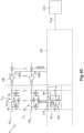
- FIG. 4C A preferred embodiment for placing cells in a metastable state while limiting matrix consumption is illustrated in Figure Figure 4C .
- a control circuit 120 producing in particular the control signals for the switches 160, 180 and for activating the transistors applied to the word lines WL 0 ,..., WL n-1 is represented schematically on the figures 4A-4C . It may be formed from a set of logic gates and may also include one or more flip-flops, and/or multiplexer(s), and/or delay stage(s).
- the circuit 120 is intended in particular to receive as input one or more signals coming from a PUF controller module 210.
- the PUF controller module 210 can be in the form of a dedicated digital circuit or in the form of a digital function produced by a processor.
- the transition from an operating mode in which the cells are in a metastable state to an operating mode in which the cells can be accessed for reading, and possibly for other operations, can be triggered in particular by a signal S PUF of request for access to the first set E1 of cells.
- the PUF controller module 210 transmits to the control circuit the signal S PUF .
- This signal S PUF makes it possible to trigger the performance of various operations including in particular at least one free initialization operation of the internal nodes of the cells of the first set E1 and possibly a biased initialization as described below.
- the internal nodes N T , N F of the cells are established at distinct respective potentials, from which it results that values are stored in memory in the PUF zone and that it is possible to read them.
- An initialization phase therefore consists of moving a memory cell from an “indeterminate” (and indeterminable by reading) or “metastable” state to a state with a “determined” stored value (and therefore determinable by reading).
- An initialization phase can be carried out when the memory device is powered on or following an erasure operation having for example been triggered following detection of fraudulent access to memory.
- a so-called “free” initialization mode consists of letting each memory cell initialize itself to its own value during the progressive energization of the elements constituting the memory cell, in particular the two looped inverters (see above in connection with the figures 2 and 3 ), without trying to impose a value “0” or “1” on the internal nodes N T and N F of the cell.
- the access transistors TA T and TA F are first not conducting, and the high power supply line VirVdd is set to the power supply potential Vdd in order to power the first inverter and the second inverter.
- a so-called deterministic initialization mode consists of imposing or forcing a value to be memorized by the cell when it passes from an indeterminate state to a determined state.
- the memory device comprises at the bottom of the column means for imposing a value on the internal nodes of the cells being initialized, via the bit lines and by making the access transistors of of the cells concerned.
- the initialization value that we wish to impose may be “0” or “1”.
- the deterministic initialization means described in this second application, in particular in connection with the Figure 4 allow all memory cells to be written either to “0” or to “1”.
- the device plans to control, for each column, one of the bit lines BL T or BL F by connecting it to a supply voltage by switching on a bit line selection transistor.
- the selected and powered bit line thus tends to impose a value “1” on one of the nodes of each memory cell connected to this bit line.
- a biased initialization mode is also described in connection with its figure 6.
- this biased initialization mode as for a deterministic initialization, a different polarization is ensured between the first bit line BLT and the second bit line BLF while activating the access transistors TA T and TA F of the initialized cells.
- a voltage Vdd or Gnd to the bit lines BL T and BL F to “force” an initialization value
- a voltage Gnd can be applied to one of the bit lines and Gnd+ ⁇ V to the other bit line.
- the biased initialization mode we only seek to “unbalance” the memory cells by favoring the switching of each memory cell towards a predefined stored value (“1” or “0”), but without necessarily forcing the switching of memory cells to this predefined state.
- the advantage of this biased initialization mode is that it makes it possible to quickly detect cells which are naturally initialized (during free initialization) to “1” or “0” with a high probability.
- a cell has, for example, a high probability of initializing at “1” during a free initialization, it can still be initialized at “1” during a biased initialization favoring writing to “0”, by “resisting” the imbalance more than another memory cell which would have a lower probability of initializing to “1” during a free initialization.
- FIG. 5 gives an example of an operating timing diagram for a memory device as described above.
- the time scale on this chronogram is not represented in a linear manner, the ratio of durations respectively between instants t1 and t2 and between instants t2 and 3 being typically much greater than in this schematic representation.
- the cells of the first set E1 are preferably maintained in a metastable state.
- their high power supply line VirVdd is disconnected from this gate or conductive line 170 and/or their internal nodes N T and N F are connected to each other, for example by activating their access transistors.
- TA T and TA F and connecting between they the bit lines BLTi, ..., BLFi via the switching element 180.
- the internal nodes N T and N F of the cells of the first set are then maintained at equal or substantially equal potentials (ie at values which differ by less than 10 mV).
- a reading circuit for example equipped with a detection amplifier at the bottom of the column, is then not capable of detecting the difference in potentials between the internal nodes N T and N F of the cells of the first set.
- initialization of the cells making it possible to maintain a metastable state of the cells during power-up requires providing a device for controlling the memory device ensuring the equivalent of a short circuit between the internal nodes NT and NF of each cell.
- the control circuit of the memory device can use all or part of the “short-circuit” or “erasure” means described in relation to the figures 2 to 4 .
- the memory cells of the set E1 initialize freely, as is conventionally done. It is also possible, according to another variant, for the memory cells of the assembly E1 to be initialized, during this power-up phase (between t0 and t1), according to a deterministic initialization mode, for example to put all cells at “0” or “1”.
- the cells of the second set E2 are powered, therefore with their upper power line connected to the grid or conductive line 170.
- the cells of this set E2 will initialize according to the initialization mode provided for power-up .
- the initialization of the cells of the set E2 are initialized to predefined values using a deterministic initialization device for example such as that described in the second aforementioned application.
- the device is in a so-called “normal” operating mode, which corresponds to a majority of the overall operating time of the matrix when it is powered, for example at minus 99% and in this example 99.9% of the time when the power supply conductive grid is powered and thus set to the supply voltage VDD.
- the cells of the first set E1 are maintained in their metastable state while the cells of the second set E2 are kept accessible for reading/writing, in particular as long as no fraudulent access is detected.
- phase t2 another phase called “PUF access” is triggered.
- the triggering of this phase can be initiated by the PUF controller module 210 which, via the signal S PUF which changes state, makes it possible to trigger the transition into a second operating mode of the cells of the first set E1.
- This second mode of operation may in particular be a mode of operation in which one wishes to access the cells of the first set in order to carry out an enrollment procedure to determine the cells which one wishes to use to create a digital signature and/or a encryption key (PUF), or in order to read a digital signature and/or an encryption key contained in certain cells of this first set E1 (the enrollment procedure having already been carried out).
- PAF digital signature and/or a encryption key
- an enrollment procedure for PUF search typically requires carrying out a large number of free initializations of the PUF zone E1 in order to establish statistics for each cell establishing a free initialization probability at “1” or “0”. Following the completion of this statistic, a choice of cells is made to form the PUF by retaining the cells presenting the highest probabilities of freely initializing to “1” or “0”.
- phase ⁇ 1 For this access to the PUF, we initialize (phase ⁇ 1) the cells of the first set E1, for example by carrying out a “free” initialization. For this, the access transistors are then non-conducting and the bit lines BLTi, ..., BLFi are disconnected from each other by means of the switching element 180 made blocked.
- the switch element 160 is made so as to connect the high power supply line VirVdd to the power grid.
- a fraudulent access detection module can then be provided to transmit to the control circuit a fraudulent access detection signal making it possible to once again trigger the passage of the cells into a metastable state.
- Such a fraudulent access detection module can be equipped with functions similar to those of a TAMP module present in an STM32GO microcontroller marketed by the company STMicroelectronics and described in the notice “STM32GO - TAMP, tamper and back-up registers, revision 1.0”.
- STM32GO - TAMP, tamper and back-up registers, revision 1.0 the cells of the first set E1 can be placed again in a metastable state by equalization of its internal nodes and/or extinction of their power supply.
- the search process is resumed including initialization and erasing operations of the cells of the first set E1 (phase ⁇ 3)
- a new change of state of the signal transmitted S PUF by the PUF controller module 210 can, from a time t3, make it possible to return to a “normal” operating mode in which the cells of the first set are put back into the metastable state.
- This change of state of the S PUF signal occurs in particular at the end of an enrollment operation or at the end of an “interrogation” or “challenge” operation of the PUF zone.
- the cells of the PUF memory are therefore maintained in a metastable state in the present invention.
- the advantage of maintaining the cells in a metastable state is to eliminate, or at least very significantly reduce, the NBTI phenomenon described previously.
- the PUF zone is protected against the effects of aging and its reliability is much greater and maintained over time.
Landscapes
- Engineering & Computer Science (AREA)
- Computer Hardware Design (AREA)
- Microelectronics & Electronic Packaging (AREA)
- Computer Security & Cryptography (AREA)
- Theoretical Computer Science (AREA)
- Software Systems (AREA)
- Physics & Mathematics (AREA)
- General Engineering & Computer Science (AREA)
- General Physics & Mathematics (AREA)
- Static Random-Access Memory (AREA)
Applications Claiming Priority (1)
| Application Number | Priority Date | Filing Date | Title |
|---|---|---|---|
| FR2214117A FR3144403B1 (fr) | 2022-12-21 | 2022-12-21 | Sram avec mise en veille de secteur dedie au puf |
Publications (1)
| Publication Number | Publication Date |
|---|---|
| EP4390930A1 true EP4390930A1 (de) | 2024-06-26 |
Family
ID=86272563
Family Applications (1)
| Application Number | Title | Priority Date | Filing Date |
|---|---|---|---|
| EP23218362.4A Pending EP4390930A1 (de) | 2022-12-21 | 2023-12-19 | Sram mit puf-different-sektor-aufrechterhaltung |
Country Status (3)
| Country | Link |
|---|---|
| US (1) | US12597464B2 (de) |
| EP (1) | EP4390930A1 (de) |
| FR (1) | FR3144403B1 (de) |
Families Citing this family (1)
| Publication number | Priority date | Publication date | Assignee | Title |
|---|---|---|---|---|
| US20240413100A1 (en) * | 2023-06-09 | 2024-12-12 | Taiwan Semiconductor Manufacturing Company, Ltd. | Stacked transistor physically unclonable function |
Citations (4)
| Publication number | Priority date | Publication date | Assignee | Title |
|---|---|---|---|---|
| FR2111286A5 (de) | 1970-10-15 | 1972-06-02 | Unitecta Oberflaechenschutz | |
| US20060023521A1 (en) * | 2004-07-29 | 2006-02-02 | International Business Machines Corporation | Method and apparatus for initializing sram device during power-up |
| US9608827B1 (en) * | 2016-01-18 | 2017-03-28 | Xilinx, Inc. | Memory cell with de-initialization circuitry |
| US20200014547A1 (en) * | 2018-07-03 | 2020-01-09 | Taiwan Semiconductor Manufacturing Co., Ltd. | Method and apparatus for noise injection for puf generator characterization |
Family Cites Families (3)
| Publication number | Priority date | Publication date | Assignee | Title |
|---|---|---|---|---|
| US8767445B2 (en) * | 2011-03-08 | 2014-07-01 | Arizona Board of Regents for and on behalf of Arizone State University | SRAM circuits for circuit identification using a digital fingerprint |
| FR3074604B1 (fr) | 2017-12-06 | 2020-01-03 | Commissariat A L'energie Atomique Et Aux Energies Alternatives | Memoire sram a effacement rapide |
| FR3128570B1 (fr) | 2021-10-25 | 2023-10-27 | Commissariat Energie Atomique | Sram a initialisation reconfigurable |
-
2022
- 2022-12-21 FR FR2214117A patent/FR3144403B1/fr active Active
-
2023
- 2023-12-19 EP EP23218362.4A patent/EP4390930A1/de active Pending
- 2023-12-19 US US18/544,789 patent/US12597464B2/en active Active
Patent Citations (4)
| Publication number | Priority date | Publication date | Assignee | Title |
|---|---|---|---|---|
| FR2111286A5 (de) | 1970-10-15 | 1972-06-02 | Unitecta Oberflaechenschutz | |
| US20060023521A1 (en) * | 2004-07-29 | 2006-02-02 | International Business Machines Corporation | Method and apparatus for initializing sram device during power-up |
| US9608827B1 (en) * | 2016-01-18 | 2017-03-28 | Xilinx, Inc. | Memory cell with de-initialization circuitry |
| US20200014547A1 (en) * | 2018-07-03 | 2020-01-09 | Taiwan Semiconductor Manufacturing Co., Ltd. | Method and apparatus for noise injection for puf generator characterization |
Non-Patent Citations (3)
| Title |
|---|
| J. MCMAHAN ET AL.: "Challenging On-Chip SRAMSecurity with Boot-State Statistics", HOST, 2017 |
| S. KUMAR ET AL.: "Impact of NBTI on SRAM Read Stability and Design for Reliability", ISQED, 2006 |
| W.-G. HO ET AL.: "A Secure Data-Toggling SRAM for Confidential Data Protection", IEEE TCAS-I, 2019 |
Also Published As
| Publication number | Publication date |
|---|---|
| US20240203485A1 (en) | 2024-06-20 |
| FR3144403A1 (fr) | 2024-06-28 |
| US12597464B2 (en) | 2026-04-07 |
| FR3144403B1 (fr) | 2025-07-25 |
Similar Documents
| Publication | Publication Date | Title |
|---|---|---|
| JP7724898B2 (ja) | フラッシュメモリデバイスのためのハッキング防止メカニズム | |
| US20180191512A1 (en) | Physically unclonable function generation with direct twin cell activation | |
| US20180287793A1 (en) | Random number generation with unstable bit states of non-volatile memory | |
| CN110678925A (zh) | 用于检测存储器的刷新不足的设备及方法 | |
| US10073989B2 (en) | Systems and methods for preventing data remanence in memory systems | |
| TW201814696A (zh) | 基於靜態隨機存取記憶體的認證電路 | |
| EP4170655A1 (de) | Sram mit rekonfigurierbarer initialisierung | |
| EP3496101A1 (de) | Sram-speicher mit schneller löschfunktion | |
| EP3633677A1 (de) | Imc-speicherschaltkreis mit 6t-zellen | |
| EP4390930A1 (de) | Sram mit puf-different-sektor-aufrechterhaltung | |
| EP3373303A1 (de) | Tfet-speicherlatch ohne aktualisierung | |
| Noel et al. | A near-instantaneous and non-invasive erasure design technique to protect sensitive data stored in secure SRAMs | |
| FR3153183A1 (fr) | Dispositif ameliore de gestion d’initialisation de memoire sram | |
| EP4390929A1 (de) | Sram-speicher mit deterministischer zufallsinitialisierung | |
| EP3680904A1 (de) | Detektionsschaltkreis eines vorherrschenden dateninhalts in einer speicherzelle | |
| EP3594951B1 (de) | Sram-/rom-speicher, der durch substratvorspannung rekonfigurierbar ist | |
| TWI658698B (zh) | 自我追蹤雙穩態閂鎖單元及自我追蹤雙穩態閂鎖單元的操作方法 | |
| EP4539390A1 (de) | Kryptographische schlüsselerzeugung aus einem sram-speicher |
Legal Events
| Date | Code | Title | Description |
|---|---|---|---|
| PUAI | Public reference made under article 153(3) epc to a published international application that has entered the european phase |
Free format text: ORIGINAL CODE: 0009012 |
|
| STAA | Information on the status of an ep patent application or granted ep patent |
Free format text: STATUS: REQUEST FOR EXAMINATION WAS MADE |
|
| 17P | Request for examination filed |
Effective date: 20231219 |
|
| AK | Designated contracting states |
Kind code of ref document: A1 Designated state(s): AL AT BE BG CH CY CZ DE DK EE ES FI FR GB GR HR HU IE IS IT LI LT LU LV MC ME MK MT NL NO PL PT RO RS SE SI SK SM TR |
|
| RAP3 | Party data changed (applicant data changed or rights of an application transferred) |
Owner name: COMMISSARIAT A L'ENERGIE ATOMIQUE ET AUX ENERGIESALTERNATIVES |