EP4391016A1 - Unité de mémoire à changement de phase et mémoire à changement de phase - Google Patents
Unité de mémoire à changement de phase et mémoire à changement de phase Download PDFInfo
- Publication number
- EP4391016A1 EP4391016A1 EP22866768.9A EP22866768A EP4391016A1 EP 4391016 A1 EP4391016 A1 EP 4391016A1 EP 22866768 A EP22866768 A EP 22866768A EP 4391016 A1 EP4391016 A1 EP 4391016A1
- Authority
- EP
- European Patent Office
- Prior art keywords
- phase change
- hafnium
- material layer
- change material
- electrode
- Prior art date
- Legal status (The legal status is an assumption and is not a legal conclusion. Google has not performed a legal analysis and makes no representation as to the accuracy of the status listed.)
- Pending
Links
Images



Classifications
-
- H—ELECTRICITY
- H10—SEMICONDUCTOR DEVICES; ELECTRIC SOLID-STATE DEVICES NOT OTHERWISE PROVIDED FOR
- H10N—ELECTRIC SOLID-STATE DEVICES NOT OTHERWISE PROVIDED FOR
- H10N70/00—Solid-state devices having no potential barriers, and specially adapted for rectifying, amplifying, oscillating or switching
- H10N70/801—Constructional details of multistable switching devices
- H10N70/881—Switching materials
- H10N70/882—Compounds of sulfur, selenium or tellurium, e.g. chalcogenides
-
- H—ELECTRICITY
- H10—SEMICONDUCTOR DEVICES; ELECTRIC SOLID-STATE DEVICES NOT OTHERWISE PROVIDED FOR
- H10N—ELECTRIC SOLID-STATE DEVICES NOT OTHERWISE PROVIDED FOR
- H10N70/00—Solid-state devices having no potential barriers, and specially adapted for rectifying, amplifying, oscillating or switching
- H10N70/801—Constructional details of multistable switching devices
- H10N70/881—Switching materials
- H10N70/882—Compounds of sulfur, selenium or tellurium, e.g. chalcogenides
- H10N70/8828—Tellurides, e.g. GeSbTe
-
- H—ELECTRICITY
- H10—SEMICONDUCTOR DEVICES; ELECTRIC SOLID-STATE DEVICES NOT OTHERWISE PROVIDED FOR
- H10B—ELECTRONIC MEMORY DEVICES
- H10B63/00—Resistance change memory devices, e.g. resistive RAM [ReRAM] devices
- H10B63/10—Phase change RAM [PCRAM, PRAM] devices
-
- H—ELECTRICITY
- H10—SEMICONDUCTOR DEVICES; ELECTRIC SOLID-STATE DEVICES NOT OTHERWISE PROVIDED FOR
- H10B—ELECTRONIC MEMORY DEVICES
- H10B63/00—Resistance change memory devices, e.g. resistive RAM [ReRAM] devices
- H10B63/20—Resistance change memory devices, e.g. resistive RAM [ReRAM] devices comprising selection components having two electrodes, e.g. diodes
- H10B63/24—Resistance change memory devices, e.g. resistive RAM [ReRAM] devices comprising selection components having two electrodes, e.g. diodes of the Ovonic threshold switching type
-
- H—ELECTRICITY
- H10—SEMICONDUCTOR DEVICES; ELECTRIC SOLID-STATE DEVICES NOT OTHERWISE PROVIDED FOR
- H10B—ELECTRONIC MEMORY DEVICES
- H10B63/00—Resistance change memory devices, e.g. resistive RAM [ReRAM] devices
- H10B63/80—Arrangements comprising multiple bistable or multi-stable switching components of the same type on a plane parallel to the substrate, e.g. cross-point arrays
-
- H—ELECTRICITY
- H10—SEMICONDUCTOR DEVICES; ELECTRIC SOLID-STATE DEVICES NOT OTHERWISE PROVIDED FOR
- H10N—ELECTRIC SOLID-STATE DEVICES NOT OTHERWISE PROVIDED FOR
- H10N70/00—Solid-state devices having no potential barriers, and specially adapted for rectifying, amplifying, oscillating or switching
- H10N70/20—Multistable switching devices, e.g. memristors
- H10N70/231—Multistable switching devices, e.g. memristors based on solid-state phase change, e.g. between amorphous and crystalline phases, Ovshinsky effect
-
- H—ELECTRICITY
- H10—SEMICONDUCTOR DEVICES; ELECTRIC SOLID-STATE DEVICES NOT OTHERWISE PROVIDED FOR
- H10N—ELECTRIC SOLID-STATE DEVICES NOT OTHERWISE PROVIDED FOR
- H10N70/00—Solid-state devices having no potential barriers, and specially adapted for rectifying, amplifying, oscillating or switching
- H10N70/801—Constructional details of multistable switching devices
- H10N70/821—Device geometry
- H10N70/826—Device geometry adapted for essentially vertical current flow, e.g. sandwich or pillar type devices
-
- H—ELECTRICITY
- H10—SEMICONDUCTOR DEVICES; ELECTRIC SOLID-STATE DEVICES NOT OTHERWISE PROVIDED FOR
- H10N—ELECTRIC SOLID-STATE DEVICES NOT OTHERWISE PROVIDED FOR
- H10N70/00—Solid-state devices having no potential barriers, and specially adapted for rectifying, amplifying, oscillating or switching
- H10N70/801—Constructional details of multistable switching devices
- H10N70/841—Electrodes
-
- H—ELECTRICITY
- H10—SEMICONDUCTOR DEVICES; ELECTRIC SOLID-STATE DEVICES NOT OTHERWISE PROVIDED FOR
- H10N—ELECTRIC SOLID-STATE DEVICES NOT OTHERWISE PROVIDED FOR
- H10N70/00—Solid-state devices having no potential barriers, and specially adapted for rectifying, amplifying, oscillating or switching
- H10N70/801—Constructional details of multistable switching devices
- H10N70/841—Electrodes
- H10N70/8413—Electrodes adapted for resistive heating
-
- Y—GENERAL TAGGING OF NEW TECHNOLOGICAL DEVELOPMENTS; GENERAL TAGGING OF CROSS-SECTIONAL TECHNOLOGIES SPANNING OVER SEVERAL SECTIONS OF THE IPC; TECHNICAL SUBJECTS COVERED BY FORMER USPC CROSS-REFERENCE ART COLLECTIONS [XRACs] AND DIGESTS
- Y02—TECHNOLOGIES OR APPLICATIONS FOR MITIGATION OR ADAPTATION AGAINST CLIMATE CHANGE
- Y02D—CLIMATE CHANGE MITIGATION TECHNOLOGIES IN INFORMATION AND COMMUNICATION TECHNOLOGIES [ICT], I.E. INFORMATION AND COMMUNICATION TECHNOLOGIES AIMING AT THE REDUCTION OF THEIR OWN ENERGY USE
- Y02D10/00—Energy efficient computing, e.g. low power processors, power management or thermal management
Definitions
- This application relates to the field of storage technologies, and in particular, to a phase change storage unit and a phase change memory.
- phase change memory phase change memory
- PCM phase change memory
- a phase change memory as one of the most promising non-volatile storage technologies for application, has been used in a plurality of storage structure directions.
- a two-dimensional phase change memory has been used in an embedded application.
- a three-dimensional phase change memory as a storage class memory (storage class memory), has been used in a scenario such as a data center.
- the phase change memory has advantages such as low power consumption, high density, and a small size, and implements data reading and writing through a conductivity difference shown when a phase change material changes between a crystalline state and an amorphous state in an electrical pulse manner.
- the phase change material is mainly a material of Ge x Sb y Te 1-x-y . Because a nucleation center of the material of Ge x Sb y Te 1-x-y in the amorphous state is unstable, a nucleation step in a crystallization process is slow, and a SET operation speed is slow.
- This application provides a phase change storage unit and a phase change memory, so as to improve a SET operation speed of the phase change memory and improve cycling performance of the phase change memory.
- this application provides a phase change storage unit, where the phase change storage unit includes a first electrode, a second electrode, and a phase change material layer.
- the phase change material layer is located between the first electrode and the second electrode, the phase change material layer includes a parent phase change material doped with a hafnium (Hf) metal and/or a hafnium compound, and the parent phase change material is a material including at least one of elements of germanium (Ge), antimony (Sb), tellurium (Te), and bismuth (Bi).
- the phase change material layer includes the parent phase change material doped with the hafnium metal and/or the hafnium compound, and the hafnium metal and/or the hafnium compound may be used as a crystal nucleus in a crystallization process, to accelerate a crystallization process of the phase change material layer, thereby improving a SET operation speed.
- the doped hafnium metal and/or hafnium compound may fill a vacancy when the parent phase change material is in a crystalline state, to reduce a volume change of the phase change material layer before and after a phase change, thereby reducing generation of a void and improving cycling performance.
- an atomic percentage of the hafnium metal and/or the hafnium compound in the phase change material layer is 0.1% to 40%.
- the atomic percentage of the hafnium metal and/or the hafnium compound in the phase change material layer is 0.1% to 40%, so that a crystallization speed of the phase change material layer can be increased, and the cycling performance can be improved.
- the following provides several examples of the atomic percentage of the hafnium metal and/or the hafnium compound in the phase change material layer:
- All the three examples can improve the crystallization speed of the phase change material layer and improve the cycling performance.
- the crystallization speed is sequentially Example 3, Example 2, and Example 1 in ascending order, and a quantity of cycles is sequentially Example 1, Example 2, and Example 3 in ascending order.
- a higher crystallization speed indicates better performance of the phase change material layer, and a higher quantity of cycles indicates better performance of the phase change material layer. Therefore, the performance of the phase change material layer in the three examples has respective advantages and disadvantages.
- the parent phase change material includes any one of the following materials: Ge x Sb y Te 1-x-y and Ge x Bi y Te 1-x-y , where a value range of a sum of x and y is 0 to 100%.
- the hafnium compound includes at least one of the following: a hafnium metal oxide, a hafnium metal boride, a hafnium metal carbide, a hafnium metal nitrogen compound, a hafnium metal sulfur compound, a hafnium metal halogen compound, and a binary or multi-ary compound formed by a hafnium metal and another metal.
- the phase change storage unit may further include a gating material layer, and the gating material layer is located between the first electrode and the second electrode.
- a specific disposition location of the gating material layer is not limited in this application.
- the gating material layer may be in a high resistance state at a low voltage, so as to suppress a leakage current, and may be in a low resistance state at a high voltage, so as to provide a sufficient current for read and write operations.
- the phase change storage unit may further include at least one of the following layers located between the first electrode and the second electrode: an insulation layer, a heating layer, an adhesion layer, and a buffer layer.
- the insulation layer When the insulation layer is specifically disposed, the insulation layer may wrap an exposed surface of the phase change material layer, and the insulation layer is non-conductive. In this case, a current passes through the phase change material layer in a centralized manner, so that current density and current heating efficiency can be improved.
- a specific disposition location of the insulation layer is not limited in this application.
- the heating layer may be disposed between any two layers between the first electrode and the second electrode.
- the heating layer is disposed between the first electrode and the phase change material layer.
- the heating layer is disposed between the phase change material layer and the second electrode.
- a specific disposition location of the heating layer is not limited in this application. The heating layer can improve a resistance of the entire unit, thereby improving the heating efficiency of the unit current.
- the adhesion layer may be disposed between any two layers between the first electrode and the second electrode.
- a specific disposition location of the adhesion layer is not limited in this application.
- the adhesion layer can improve an adhesion effect between two layers adjacent to the adhesion layer.
- the buffer layer When the buffer layer is specifically disposed, the buffer layer may be disposed between any two layers between the first electrode and the second electrode. A specific disposition location of the buffer layer is not limited in this application.
- the buffer layer can reduce mutual diffusion of two adjacent material layers in the phase change storage unit in repeated erase and write (or reset/set) operations, thereby improving reliability.
- the phase change material layer is prepared by using a chemical vapor deposition method, physical vapor deposition, or atomic layer deposition.
- this application provides another phase change storage unit, where the phase change storage unit includes a first electrode, a second electrode, and a phase change material layer.
- the phase change material layer is located between the first electrode and the second electrode, the phase change material layer includes at least one hafnium-containing material layer and at least one sulfur compound material layer that are laminated, the hafnium-containing material layer includes at least one of the following materials: a hafnium (Hf) metal, a hafnium compound, a parent phase change material doped with the hafnium metal and/or the hafnium compound, and the parent phase change material is a material including at least one of elements of germanium (Ge), antimony (Sb), tellurium (Te), and bismuth (Bi).
- the phase change material layer includes the at least one hafnium-containing material layer and the at least one sulfur compound material layer that are laminated, and the doped hafnium metal and/or hafnium compound included in the hafnium-containing material layer may be used as a crystal nucleus in a crystallization process, to accelerate a crystallization process, thereby improving a SET operation speed.
- the phase change material layer includes at least two layers of laminated structures, so that thermal conductivity of the phase change storage unit is changed, and an interface between the two material layers hinders heat conduction.
- the sulfur compound material layer further helps to suppress a low-resistance failure caused by conduction between upper and lower electrodes caused by element segregation in the hafnium-containing material layer, thereby improving the cycling performance of the phase change storage unit, and helping reduce a resistance drift.
- the sulfur compound material layer includes at least one of the following materials: a tellurium compound of a tellurium (Te) element and at least one of elements of germanium (Ge), antimony (Sb), titanium (Ti), tantalum (Ta), scandium (Sc), bismuth (Bi), silicon (Si), carbon (C), platinum (Pt), and indium (In) and a tellurium compound doped with a hafnium metal and/or a hafnium compound.
- a tellurium compound of a tellurium (Te) element and at least one of elements of germanium (Ge), antimony (Sb), titanium (Ti), tantalum (Ta), scandium (Sc), bismuth (Bi), silicon (Si), carbon (C), platinum (Pt), and indium (In) and a tellurium compound doped with a hafnium metal and/or a hafnium compound.
- the parent phase change material includes any one of the following materials: Ge x Sb y Te 1-x-y , Ge x Bi y Te 1-x-y , and Sb x Te y , where a value range of a sum of x and y is 0 to 100%.
- the hafnium-containing material layer and the sulfur compound material layer that are included in the phase change material layer are alternately arranged.
- a simple substance precipitated from the hafnium-containing material layer may be combined with a material in a sulfur compound material layer adjacent to the hafnium-containing material layer, so that the low-resistance failure caused by conduction of the entire phase change material layer can be effectively suppressed, thereby improving the cycling performance of the phase change storage unit, and reducing the resistance drift.
- the phase change material layer includes at least three material layers that are laminated, the at least three material layers include at least one hafnium-containing material layer and at least one sulfur compound material layer, and the hafnium-containing material layer and the sulfur compound material layer that are included in the at least three material layers are alternately arranged.
- the at least three material layers include at least one hafnium-containing material layer and at least one sulfur compound material layer, and the hafnium-containing material layer and the sulfur compound material layer that are included in the at least three material layers are alternately arranged.
- the phase change storage unit further includes a gating material layer located between the first electrode and the second electrode.
- a specific disposition location of the gating material layer is not limited in this application.
- the gating material layer may be in a high resistance state at a low voltage, so as to suppress a leakage current, and may be in a low resistance state at a high voltage, so as to provide a sufficient current for read and write operations.
- the phase change storage unit may further include at least one of the following layers located between the first electrode and the second electrode: an insulation layer, an electrode layer, a heating layer, an adhesion layer, and a buffer layer.
- the insulation layer When the insulation layer is specifically disposed, the insulation layer may wrap an exposed surface of the phase change material layer, and the insulation layer is non-conductive. In this case, a current passes through the phase change material layer in a centralized manner, so that current density and current heating efficiency can be improved.
- a specific disposition location of the insulation layer is not limited in this application.
- the electrode layer When the electrode layer is specifically disposed, the electrode layer may be disposed between any two layers between the first electrode and the second electrode.
- a specific disposition location of the electrode layer is not limited in this application.
- the heating layer may be disposed between any two layers between the first electrode and the second electrode.
- the heating layer is disposed between the first electrode and the phase change material layer.
- the heating layer is disposed between the phase change material layer and the second electrode.
- a specific disposition location of the heating layer is not limited in this application. The heating layer can improve a resistance of the entire unit, thereby improving the heating efficiency of the unit current.
- the adhesion layer may be disposed between any two layers between the first electrode and the second electrode.
- a specific disposition location of the adhesion layer is not limited in this application.
- the adhesion layer can improve an adhesion effect between two layers adjacent to the adhesion layer.
- the buffer layer When the buffer layer is specifically disposed, the buffer layer may be disposed between any two layers between the first electrode and the second electrode. A specific disposition location of the buffer layer is not limited in this application.
- the buffer layer can reduce mutual diffusion of two adjacent material layers in the phase change storage unit in repeated erase and write (or reset/set) operations, thereby improving reliability.
- the phase change material layer is prepared by using a chemical vapor deposition method, a physical vapor deposition method, or an atomic layer deposition method.
- this application provides a phase change memory, including a controller and a storage medium, where the storage medium includes an array including the phase change storage unit in the first aspect and the possible implementations of the first aspect, or an array including the phase change storage unit in the second aspect and the possible implementations of the second aspect.
- the phase change memory provided in this application may be configured to store data in an electronic device such as a mobile phone, a tablet computer, a notebook computer, a wearable device, or an in-vehicle device.
- the phase change memory is a non-volatile memory based on a sulfur phase change material, and can be converted in different resistance states in a heat action.
- Data 0 and data 1 are stored by using a difference of 10 to 10000 times a resistance value between a high resistance state (a reset state) and a low resistance state (a set state) of the phase change memory.
- a set operation is an operation from the high resistance state to the low resistance state
- a reset operation is an operation from the low resistance state to the high resistance state.
- a phase change material is mainly a material of Ge x Sb y Te 1-x-y. Because a nucleation center of the material of Ge x Sb y Te 1-x-y in an amorphous state is unstable, a nucleation step in a crystallization process is slow, and a SET operation speed is slow. In addition, a density difference of the material of Ge x Sb y Te 1-x-y in a crystalline state and the amorphous state is large, a material volume changes repeatedly in a cyclic operation process, and it is easy to cause generation of a void. As a result, cycling performance is poor. To resolve the foregoing problem, this application provides a phase change storage unit and a phase change memory. The following describes the phase change storage unit and the phase change memory in the technical solutions of this application with reference to the accompanying drawings.
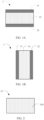
- FIG. 1A is a schematic diagram of a structure of a phase change storage unit according to an embodiment of this application.
- a phase change storage unit 1 in this embodiment of this application includes a first electrode 11, a second electrode 12, and a phase change material layer 13.
- the phase change material layer 13 is located between the first electrode 11 and the second electrode 12.
- first electrode 11 and the second electrode 12 in this embodiment of this application may be in an up-down structure shown in FIG. 1A .
- the first electrode 11 is above the second electrode 12 in a vertical direction.
- the first electrode 11 may alternatively be below the second electrode 12 in the vertical direction. This is not limited in this embodiment of this application.
- the first electrode 11 and the second electrode 12 may be in a left-right structure shown in FIG. 1B .
- the first electrode 11 is on the left of the second electrode 12 in a horizontal direction. It should be understood that in some other embodiments, the first electrode 11 may alternatively be on the right of the second electrode 12 in the horizontal direction.
- first electrode 11 and the second electrode 12 in FIG. 11 , FIG. 13, and FIG. 13 below may be the up-down structure in the vertical direction or the left-right structure in the vertical direction. Details are not described in the following.
- the first electrode 11 and the second electrode 12 are schematically described by using the up-down structure in the vertical direction. Details are not described in the following.
- the phase change material layer 13 has a first resistance state and a second resistance state, and a resistance value of the phase change material layer 13 in the first resistance state is different from a resistance value of the phase change material layer 13 in the second resistance state, so that read and write operations may be performed by controlling and reading a current resistance value of the phase change storage unit 1. It should be understood that the phase change material layer 13 may have more than two resistance states, and may have a plurality of resistance states. A quantity of resistance states of the phase change material layer 13 is not limited in this application.
- the phase change material layer 13 may have a plurality of possible implementations, which are separately described below.
- FIG. 2 is a schematic diagram of a vertical cross section of a phase change material layer 13 including one material layer according to an embodiment of this application.
- the phase change material layer 13 includes one material layer 130, where the material layer 130 includes a parent phase change material 130 doped with a hafnium (Hf) metal and/or a hafnium compound, and the parent phase change material is a material including at least one of elements of germanium (Ge), antimony (Sb), tellurium (Te), and bismuth (Bi).
- a local crystalline structure of the hafnium metal and/or the hafnium compound is consistent with a local crystalline structure of a matrix material.
- atomic percentages of different parts of the hafnium-containing or the hafnium-containing compound in the phase change material are inconsistent.
- the atomic percentages of the hafnium-containing or the hafnium-containing compound in the phase change material are in a gradient change from high to low or from low to high in a direction from the top electrode to the bottom electrode.
- an atomic percentage of the hafnium metal and/or the hafnium compound in the phase change material layer 13 is 0.1% to 40%.
- the atomic percentage of the hafnium metal and/or the hafnium compound is set in this way, so that a crystallization speed of the phase change material layer can be improved, and the cycling performance can be improved.
- the following provides several examples of the atomic percentage of the hafnium metal and/or the hafnium compound in the phase change material layer:
- All the six examples can improve the crystallization speed of the phase change material layer 13 and improve the cycling performance.
- the crystallization speed is sequentially Example 3, Example 2, and Example 1 in ascending order, and a quantity of cycles is sequentially Example 1, Example 2, and Example 3 in ascending order.
- a higher crystallization speed indicates better performance of the phase change material layer, and a higher quantity of cycles indicates better performance of the phase change material layer. Therefore, the performance of the phase change material layer in the three examples has respective advantages and disadvantages.
- a specific material of the parent phase change material is not limited, and the parent phase change material may include any one of the following materials: Ge x Sb y Te 1-x-y , Ge x Bi y Te 1-x-y , Sb x Te y , Bi x Te y , Ge x Te y , and Sb, where a value range of a sum of x and y is 0 to 100%.
- the parent phase change material may further include Ge x Sb y Bi z Te 1-x-y-z , where a value range of a sum of x, y, and z is 0 to 100%.
- the parent phase change material is, for example, any one of Ge x Sb y Te 1-x-y and Ge x Bi y Te 1-x-y , where a value range of a sum of x and y is 0 to 100%.
- the parent material may be Sb x Te y , or the parent material further includes Ge x Sb y Bi z Te 1-x-y-z , where a sum of x, y, and z is 100%.
- a value range of a concentration of Ge x Sb y Te 1-x-y may be a gray elliptic region and a quadrilateral region A shown in FIG. 16 .
- the material Ge x Sb y Te 1-x-y in the region has a high-speed crystallization characteristic, and also has specific thermal stability.
- 1/7-1/10 ⁇ x:(1-x-y) ⁇ 1/4+1/10 or 2/3-1/10 ⁇ y:(1-x-y) ⁇ 2/3+1/10 1/7 ⁇ x:(1-x-y) ⁇ 2/5 and 2/3 ⁇ y:(1-x-y) ⁇ 4.
- the hafnium compound may include at least one of the following: a hafnium metal oxide (for example, HfO 2 ), a hafnium metal boride (for example, HfB), a hafnium metal carbide (for example, HfC), a hafnium metal nitride compound (for example, HfN), a hafnium metal sulfur compound (for example, HfS, HfSe, and HfTe), a hafnium metal halogen compound (for example, HfF, HfCl, and HfBr), and a binary or multi-ary compound (for example, HfTa, HfW, HfTi, and HfSc) formed by a hafnium metal and another metal.
- a hafnium metal oxide for example, HfO 2
- HfB hafnium metal boride
- HfC hafnium metal carbide
- HfN hafnium metal nitride compound
- the phase change material layer 13 may be prepared by using a deposition method.
- the deposition method may be a chemical vapor deposition (chemical vapor deposition, CVD) method, a physical vapor deposition (physical vapor deposition, PVD) method, or an atomic layer deposition (atomic layer deposition, ALD) method.
- two or more targets may be used.
- One target is an Hf-containing material
- the other target is a parent phase change material, or may be an alloy target.
- the alloy target includes both the Hf-containing material and the parent material.
- N 2 , O 2 , and the like may be further added to form a nitride or oxide.
- the phase change material layer 13 includes a plurality of material layers.
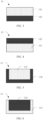
- FIG. 3 to FIG. 10 are schematic diagrams of vertical cross sections of a phase change material layer 13 including a plurality of material layers according to an embodiment of this application.
- the phase change material layer 13 includes at least one hafnium-containing material layer 131 and at least one sulfur compound material layer 132 that are laminated.
- the hafnium-containing material layer 131 includes at least one of the following materials: a hafnium (Hf) metal, a hafnium compound, a parent phase change material doped with the hafnium metal and/or the hafnium compound, and the parent phase change material is a material of at least one of elements of germanium (Ge), antimony (Sb), tellurium (Te), and bismuth (Bi).
- the phase change material layer 13 includes the at least one hafnium-containing material layer 131 and the at least one sulfur compound material layer 132 that are laminated, and the doped hafnium metal and/or hafnium compound included in the hafnium-containing material layer 131 may be used as a crystal nucleus in a crystallization process, to accelerate a crystallization process, thereby improving a SET operation speed.
- the phase change material layer 13 includes at least two layers of laminated structures, so that thermal conductivity of the phase change storage unit is changed, and an interface between the two material layers hinders heat conduction.
- the sulfur compound material layer 132 further helps to suppress a low-resistance failure caused by conduction between upper and lower electrodes caused by element segregation in the hafnium-containing material layer 131, thereby improving the cycling performance of the phase change storage unit, and helping reduce a resistance drift.
- the sulfur compound material layer 132 may include at least one of the following materials: a tellurium compound of a tellurium (Te) element and at least one of elements of germanium (Ge), antimony (Sb), titanium (Ti), tantalum (Ta), scandium (Sc), bismuth (Bi), silicon (Si), carbon (C), platinum (Pt), and indium (In), and a tellurium compound doped with a hafnium metal and/or a hafnium compound.
- the sulfur compound material layer 132 may be Ge x Te 1-x , Sb x Te 1-x , Ge x Te 1-x , Ti x Te 1-x , Ta x Te 1-x , Sc x Te 1-x , Bi x Te 1-x , Ge x Sb 1-x , In x Te 1-x , Si x Te 1-x , C x Te 1-x , Pt x Te 1-x , Ge x Sb y Te 1-x-y , Ge x Bi y Te 1-x-y , Ta x Sb y Te 1-x-y , Ti x Sb y Te 1-x-y , or Sc x Sb y Te 1-x-y , or may be an Hf-containing sulfur compound, for example, Hf x Te 1-x , Hf x Sb y Te 1-x-y , or HfGe x Sb y Te 1-x-y , or an Hf-containing material in which a concentration of a hafn
- a specific material of the parent phase change material is not limited, and the parent phase change material may include any one of the following materials: Ge x Sb y Te 1-x-y , Ge x Bi y Te 1-x-y , Sb x Te y , Bi x Te 1 , Ge x Te y , and Sb, where a value range of a sum of x and y is 0 to 100%.
- the parent phase change material may further include Ge x Sb y Bi x Te 1-x-y-z , where a value range of a sum of x, y, and z is 0 to 100%.
- the parent phase change material is, for example, any one of Ge x Sb y Te 1-x-y and Ge x Bi y Te 1-x-y.
- the hafnium compound may include at least one of the following: a hafnium metal oxide (for example, HfO 2 ), a hafnium metal boride (for example, HfB), a hafnium metal carbide (for example, HfC), a hafnium metal nitride compound (for example, HfN), a hafnium metal sulfur compound (for example, HfS, HfSe, and HfTe), a hafnium metal halogen compound (for example, HfF, HfCl, and HfBr), and a binary or multi-ary compound (for example, HfTa, HfW, HfTi, and HfSc) formed by a hafnium metal and another metal.
- a hafnium metal oxide for example, HfO 2
- HfB hafnium metal boride
- HfC hafnium metal carbide
- HfN hafnium metal nitride compound
- a material combination of the hafnium-containing material layer 131 and the sulfur compound material layer 132 may be, for example, any one of the following: HfGe x Sb y Te 1-x-y /Sb x Te 1-x , HfGe x Sb y Te 1-x-y /Ge x Sb y Te 1-x-y , HfGe x Sb y Te 1-x-y /Ge x Te 1-x , HfGe x Sb y Te 1-x-y (a concentration A)/HfGe x Sb y Te 1-x-y (a concentration B), where the concentration A is different from the concentration B, HfO 2 / HfGe x Sb y Te 1-x-y , and Hf x Te 1-x /HfGe x Sb y Te 1-x-y , and the like.
- the hafnium-containing material layer 131 and the sulfur compound material layer 132 that are included in the phase change material layer 13 are alternately arranged. In this manner, if an element segregation problem occurs in a hafnium-containing material layer 131, and the hafnium-containing material layer 131 is conducted, a simple substance precipitated from the hafnium-containing material layer 131 may be combined with a material in a sulfur compound material layer 132 adjacent to the hafnium-containing material layer 131, so that the low-resistance failure caused by conduction of the entire phase change material layer 13 can be effectively suppressed, thereby improving the cycling performance of the phase change storage unit, and reducing the resistance drift.
- the phase change material layer 13 includes a hafnium-containing material layer 131 and a sulfur compound material layer 132. As shown in FIG. 3 , the sulfur compound material layer 132 may be located below the hafnium-containing material layer 131. It may be understood that, in the phase change storage unit, the sulfur compound material layer 132 is located on a side that is of the hafnium-containing material layer 131 and that is away from the first electrode 11. As shown in FIG. 4 , the sulfur compound material layer 132 may alternatively be located above the hafnium-containing material layer 131.
- the sulfur compound material layer 132 is located on a side that is of the hafnium-containing material layer 131 and that is away from the second electrode 12. As shown in FIG. 5 , the sulfur compound material layer 132 may alternatively be located below the hafnium-containing material layer 131, and the sulfur compound material layer 132 wraps a side wall and a bottom of the hafnium-containing material layer 131. As shown in FIG. 6 , the sulfur compound material layer 132 may alternatively be located above the hafnium-containing material layer 131, and the hafnium-containing material layer 131 wraps a side wall and a bottom of the sulfur compound material layer 132.
- the phase change material layer 13 includes at least three material layers that are laminated, the at least three material layers include at least one hafnium-containing material layer 131 and at least one sulfur compound material layer 132, and the hafnium-containing material layer 131 and the sulfur compound material layer 132 that are included in the at least three material layers are alternately arranged.
- a quantity of interfaces in the phase change material layer 13 can be increased, and the thermal conductivity can be further reduced. Therefore, the heating efficiency can be improved, and the power consumption of the RESET operation can be reduced, thereby reducing the probability of generating a void and further improving the cycling performance.
- the phase change material layer 13 includes three or more material layers, and a dual-layer material layer including the hafnium-containing material layer 131 and the sulfur compound material layer 132, as a basic unit, is repeated n times, where n is an integer greater than or equal to 1. As shown in FIG. 7 , both an uppermost layer and a lowermost layer of the phase change material layer 13 are the sulfur compound material layers 132. As shown in FIG. 8 , both an uppermost layer and a lowermost layer of the phase change material layer 13 are the hafnium-containing material layers 131. As shown in FIG.
- an uppermost layer of the phase change material layer 13 is the hafnium-containing material layer 131, and a lowermost layer of the phase change material layer 13 is the sulfur compound material layer 132.
- an uppermost layer of the phase change material layer 13 is the sulfur compound material layer 132, and a lowermost layer of the phase change material layer 13 is the hafnium-containing material layer 131.
- the at least one hafnium-containing material layer 131 and the at least one sulfur compound material layer 132 included in the phase change material layer 13 may be prepared by using a deposition method.
- the deposition method may be a chemical vapor deposition method, a physical vapor deposition method, or an atomic layer deposition method.
- the phase change storage unit may further include at least one of the following layers located between the first electrode 11 and the second electrode 12: an insulation layer, a heating layer, an adhesion layer, a buffer layer, and an electrode layer.
- the insulation layer When the insulation layer is specifically disposed, the insulation layer may wrap an exposed surface of the phase change material layer 13, and the insulation layer is non-conductive. In this case, a current passes through the phase change material layer 13 in a centralized manner, so that current density and current heating efficiency can be improved.
- a specific disposition location of the insulation layer is not limited in this application.
- a material of the insulation layer may be, for example, at least one of silicon dioxide (SiO 2 ), silicon nitride (SiN), or titanium nitride (TiN), or may be another material that can isolate a current.
- a specific material of the insulation layer is not limited in this application.
- the heating layer may be disposed between any two layers between the first electrode 11 and the second electrode 12.
- the heating layer is disposed between the first electrode 11 and the phase change material layer 13.
- the heating layer is disposed between the phase change material layer 13 and the second electrode 12.
- a specific disposition location of the heating layer is not limited in this application.
- the heating layer can improve a resistance of the entire unit, thereby improving the heating efficiency of the unit current.
- the adhesion layer may be disposed between any two layers between the first electrode 11 and the second electrode 12.
- a specific disposition location of the adhesion layer is not limited in this application.
- the adhesion layer can improve an adhesion effect between two layers adjacent to the adhesion layer.
- the buffer layer When the buffer layer is specifically disposed, the buffer layer may be disposed between any two layers between the first electrode 11 and the second electrode 12. A specific disposition location of the buffer layer is not limited in this application.
- the buffer layer can reduce mutual diffusion of two adjacent material layers in the phase change storage unit in repeated erase and write (or reset/set) operations, thereby improving reliability.
- the electrode layer When the electrode layer is specifically disposed, the electrode layer may be disposed between any two layers between the first electrode 11 and the second electrode 12. A specific disposition location of the electrode layer is not limited in this application.
- materials of the heating layer, the adhesion layer, and the buffer layer may be, for example, oxide, a boron compound, a carbon compound, a nitrogen compound, a sulfur compound, and a halogen compound.
- the specific materials of the heating layer, the adhesion layer, and the buffer layer are not limited in this application, provided that corresponding functions of the material layers can be implemented.
- the phase change storage unit may further include a gating material layer, and the gating material layer is located between the first electrode 11 and the second electrode 12.
- a specific disposition location of the gating material layer is not limited in this application.
- the gating material layer may be in a high resistance state at a low voltage, so as to suppress a leakage current, and may be in a low resistance state at a high voltage, so as to provide a sufficient current for read and write operations.
- the gating material layer may include a single material layer, or may include a plurality of material layers.
- the gating material layer includes the single material layer.
- the gating material layer may include a matrix material doped with a hafnium metal and/or a hafnium compound.
- the matrix material may be, for example, Ge x As y Se(Te) 1-x-y , where a sum of x and y is equal to 1.
- the hafnium compound refer to the related descriptions of the hafnium compound in the phase change material layer 13. Details are not described herein again.
- the gating material layer may include the plurality of material layers.
- the gating material layer may include at least one hafnium-containing material layer and at least one sulfur compound material layer.
- the gating material layer may include the plurality of material layers, refer to the related descriptions of the phase change material layer including the plurality of material layers. Details are not described herein again.
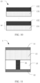
- FIG. 11 is another schematic diagram of a structure of a phase change storage unit according to an embodiment of this application.
- a phase change storage unit 1 shown in FIG. 11 is a T-type phase change storage unit.
- the phase change storage unit 1 includes a first electrode 11, a second electrode 12, and a phase change material layer 13 located between the first electrode 11 and the second electrode 12.
- the phase change storage unit 1 may further include a heating layer 16 located between the phase change material layer 13 and the second electrode 12, and an insulation layer 15 further wraps a side wall of the heating layer 16.
- the heating layer 16 needs to meet a conductive requirement, and further needs to improve a resistance effect of the entire phase change storage unit.
- FIG. 12 is another schematic diagram of a structure of a phase change storage unit according to an embodiment of this application.
- a phase change storage unit 1 shown in FIG. 12 is a restrictive phase change storage unit.
- the phase change storage unit 1 includes a first electrode 11, a second electrode 12, and a phase change material layer 13 located between the first electrode 11 and the second electrode 12.
- the phase change material layer 13 has a small cross section size, and is directly connected to the first electrode 11 above the phase change material layer 13 and the second electrode 12 below the phase change material layer 13.
- the phase change storage unit 1 may further include an insulation layer 15 located between the phase change material layer 13 and the second electrode 12, and the insulation layer 15 wraps a side wall of the phase change material layer 13.
- FIG. 13 is another schematic diagram of a structure of a phase change storage unit according to an embodiment of this application.
- a phase change storage unit 1 shown in FIG. 13 is a three-dimensional phase change storage unit.
- the phase change storage unit 1 includes a first electrode 11, a second electrode 12, and a phase change material layer 13 located between the first electrode 11 and the second electrode 12.
- the phase change material layer 13 may further include a gating material layer 14 located between the first electrode 11 and the second electrode 12. Cross section sizes of the phase change material layer 13 and the gating material layer 14 are small.
- a first electrode layer 17, the phase change material layer 13, a second electrode layer 18, the gating material layer 14, and a third electrode layer 19 are sequentially included between the first electrode 11 and the second electrode 12.
- the phase change material layer 13 may be connected to the first electrode 11 by the first electrode layer 17, and the gating material layer 14 may be connected to the phase change material layer 13 by the second electrode layer 18, and is connected to the second electrode 12 by the second electrode layer 18.
- the phase change storage unit 1 may further include an insulation layer 15 located between the phase change material layer 13 and the second electrode 12.
- the insulation layer 15 wraps the phase change material layer 13, the gating material layer 14, and side walls of the electrode layers.
- the first electrode 11 and the second electrode 12 extend in different horizontal directions, to connect different phase change storage units in a storage array to form an array arranged on one layer. Such arrays are further stacked in a vertical direction to form a cross-stacked three-dimensional phase change memory.
- FIG. 14 is a schematic diagram of a structure of a phase change memory according to an embodiment of this application.
- a phase change memory 100 includes a controller 110 and a storage medium 120.
- the storage medium 120 includes an array including the phase change storage unit 1 in any one of the foregoing embodiments.
- this application further provides a phase change memory.
- FIG. 15 is another schematic diagram of a structure of a phase change memory according to an embodiment of this application.
- the phase change memory may further include a row decoder (row decoder), a column decoder (column decoder), a sense amplifier (sense amplifier), a drive circuit (drive circuit), a data buffer (data buffer), and a digital controller (digital controller).
- First electrodes 12 of a plurality of phase change storage units 1 are connected to form a first electrode line 2
- second electrodes 13 of the plurality of phase change storage units 1 are connected to form a second electrode line 3, and an extending direction of the first electrode line 2 intersects with an extending direction of the second electrode line 3.
- phase change storage unit 1 there is a uniquely determined phase change storage unit 1 at an intersection of the first electrode line 2 and the second electrode line 3.
- the row decoder of the phase change memory is electrically connected to all first electrode lines 2, and the column decoder, the sense amplifier, and the drive circuit are electrically connected to all second electrode lines 3.
- the row decoder, the column decoder, the sense amplifier, and the drive circuit are electrically connected to the digital controller and the data buffer respectively.
- One of the first electrode line 2 and the second electrode line 3 is a word line (word line, WL), and the other of the first electrode line 2 and the second electrode line 3 is a bit line (bit line, BL), so that one word line is connected to phase change storage units 1 in one row, and a level value different from that of another word line is applied to a selected word line, so as to select phase change storage units 1 in a row to perform read and write operations and the like.
- One bit line is connected to phase change storage units 1 in one column, and transmits an electrical signal of a write operation of the phase change storage unit 1 to a column selected by the column decoder, or transmits, along a selected column, an electrical signal obtained by an operation of a reading unit to the column decoder.
- the first electrode line 2 may be used as the word line, and the second electrode line 3 may be used as the bit line; or the first electrode line 2 may be used as the bit line, and the second electrode line 3 may be used as the word line. This is not limited in this application.
- the row decoder of the phase change memory is electrically connected to all the first electrode lines 2, and the column decoder, the sense amplifier, and the drive circuit are electrically connected to all the second electrode lines 3.
- the row decoder, the column decoder, the sense amplifier, and the drive circuit are electrically connected to the digital controller and the data buffer respectively. Because there is a uniquely determined phase change storage unit 1 located at an intersection of the first electrode line 2 and the second electrode line 3, and the phase change storage unit 1 has different resistance states, read and write operations of a three-dimensional phase change memory can be implemented.
- the digital controller controls the row decoder to modulate a voltage of the first electrode line 2 connected to a set phase change storage unit 1 to a read mode (for example, a voltage is 0V), and controls the column decoder to modulate a voltage of the second electrode line 3 connected to the set phase change storage unit 1 to the read mode (for example, a voltage is 1V). Then, a current of the set phase change storage unit 1 is measured by using the sense amplifier connected to the second electrode line 3, to determine a resistance state of a phase change material layer 13 of the phase change storage unit 1, so as to obtain a data storage state.
- the digital controller controls the row decoder to modulate the voltage of the first electrode line 2 connected to the set phase change storage unit 1 to a write mode (for example, a voltage is 2V), and controls the column decoder to modulate the voltage of the second electrode line 3 connected to the set phase change storage unit 1 to the write mode (for example, a voltage is 0V), and then a write pulse current or pulse voltage is sent to the set phase change storage unit 1 by using the drive circuit connected to the second electrode line 3, to change a resistance state of the phase change storage unit 1, to implement the write operation.
- data read from the sense amplifier and data written to the phase change memory are stored in the data buffer.
- the phase change memory may be a two-dimensional phase change memory.
- the phase change storage units 1 in the two-dimensional phase change memory may be arranged in an array, for example, may be arranged in n rows and m columns, where m and n are respectively positive integers greater than 1.
Landscapes
- Semiconductor Memories (AREA)
Applications Claiming Priority (3)
| Application Number | Priority Date | Filing Date | Title |
|---|---|---|---|
| CN202111068031.7 | 2021-09-13 | ||
| CN202210863735.1A CN115811933A (zh) | 2021-09-13 | 2022-07-21 | 一种相变存储单元及相变存储器 |
| PCT/CN2022/118183 WO2023036307A1 (fr) | 2021-09-13 | 2022-09-09 | Unité de mémoire à changement de phase et mémoire à changement de phase |
Publications (2)
| Publication Number | Publication Date |
|---|---|
| EP4391016A1 true EP4391016A1 (fr) | 2024-06-26 |
| EP4391016A4 EP4391016A4 (fr) | 2025-01-01 |
Family
ID=83322381
Family Applications (1)
| Application Number | Title | Priority Date | Filing Date |
|---|---|---|---|
| EP22866768.9A Pending EP4391016A4 (fr) | 2021-09-13 | 2022-09-09 | Unité de mémoire à changement de phase et mémoire à changement de phase |
Country Status (5)
| Country | Link |
|---|---|
| US (1) | US20240268242A1 (fr) |
| EP (1) | EP4391016A4 (fr) |
| KR (1) | KR102872137B1 (fr) |
| CN (2) | CN115101667B (fr) |
| WO (1) | WO2023036307A1 (fr) |
Families Citing this family (2)
| Publication number | Priority date | Publication date | Assignee | Title |
|---|---|---|---|---|
| CN115697032A (zh) * | 2022-10-14 | 2023-02-03 | 同济大学 | 一种纳米复合堆叠相变薄膜及其制备方法与应用 |
| CN115867122A (zh) * | 2022-11-28 | 2023-03-28 | 深圳大学 | 一种阈值开关材料、阈值开关器件及其制备方法 |
Family Cites Families (10)
| Publication number | Priority date | Publication date | Assignee | Title |
|---|---|---|---|---|
| US7723712B2 (en) * | 2006-03-17 | 2010-05-25 | Micron Technology, Inc. | Reduced power consumption phase change memory and methods for forming the same |
| US7663909B2 (en) * | 2006-07-10 | 2010-02-16 | Qimonda North America Corp. | Integrated circuit having a phase change memory cell including a narrow active region width |
| KR100807230B1 (ko) * | 2006-09-27 | 2008-02-28 | 삼성전자주식회사 | 상변화 물질층 및 이를 포함하는 상변화 메모리 장치 |
| KR20130033019A (ko) * | 2011-09-26 | 2013-04-03 | 에스케이하이닉스 주식회사 | 상변화 메모리 장치 및 그의 제조방법 |
| KR102530067B1 (ko) * | 2016-07-28 | 2023-05-08 | 삼성전자주식회사 | 가변 저항 메모리 소자 및 그 제조 방법 |
| US10008665B1 (en) * | 2016-12-27 | 2018-06-26 | Intel Corporation | Doping of selector and storage materials of a memory cell |
| US11587978B2 (en) * | 2018-09-19 | 2023-02-21 | International Business Machines Corporation | Phase change memory with improved recovery from element segregation |
| CN110335942A (zh) * | 2019-07-08 | 2019-10-15 | 中国科学院上海微系统与信息技术研究所 | 一种相变存储器及其制作方法 |
| CN110931635B (zh) * | 2019-10-28 | 2021-09-14 | 华中科技大学 | 低密度变化的超晶格相变薄膜、相变存储器及其制备方法 |
| CN111320145A (zh) * | 2020-02-24 | 2020-06-23 | 中国科学院上海微系统与信息技术研究所 | 一种相变材料、相变存储器单元及其制作方法 |
-
2021
- 2021-09-13 CN CN202210585095.2A patent/CN115101667B/zh active Active
-
2022
- 2022-07-21 CN CN202210863735.1A patent/CN115811933A/zh active Pending
- 2022-09-09 WO PCT/CN2022/118183 patent/WO2023036307A1/fr not_active Ceased
- 2022-09-09 EP EP22866768.9A patent/EP4391016A4/fr active Pending
- 2022-09-09 KR KR1020247011763A patent/KR102872137B1/ko active Active
-
2024
- 2024-03-12 US US18/602,721 patent/US20240268242A1/en active Pending
Also Published As
| Publication number | Publication date |
|---|---|
| CN115101667B (zh) | 2024-10-22 |
| CN115101667A (zh) | 2022-09-23 |
| KR20240055832A (ko) | 2024-04-29 |
| EP4391016A4 (fr) | 2025-01-01 |
| WO2023036307A1 (fr) | 2023-03-16 |
| US20240268242A1 (en) | 2024-08-08 |
| CN115811933A (zh) | 2023-03-17 |
| KR102872137B1 (ko) | 2025-10-15 |
Similar Documents
| Publication | Publication Date | Title |
|---|---|---|
| US20240268242A1 (en) | Phase change storage unit and phase change memory | |
| CN113196491B (zh) | 三维存储器阵列及其处理方法 | |
| TWI453896B (zh) | 電阻式記憶胞及其操作方法,以及電阻式記憶體及其操作方法與製造方法 | |
| US8982604B2 (en) | Resistive memory device and memory apparatus and data processing system having the same | |
| US9276202B2 (en) | Phase-change storage unit containing TiSiN material layer and method for preparing the same | |
| US10734493B2 (en) | Semiconductor memory device and conductive structure | |
| US11374059B2 (en) | Memory cells having resistors and formation of the same | |
| CN103855304A (zh) | 可变电阻存储器件 | |
| KR102119306B1 (ko) | 저항 스위칭 소자 및 이를 이용한 상변화 메모리 소자 | |
| US10515695B2 (en) | Resistive memory device and method of fabricating the same | |
| US11616098B2 (en) | Three-dimensional memory arrays, and methods of forming the same | |
| TW201535477A (zh) | 用於矽基導電膜的低溫沈積 | |
| JP5940924B2 (ja) | 低電力で動作する半導体記憶装置 | |
| CN101826463B (zh) | 共用金属层的肖特基二极管和相变存储器的制造方法 | |
| CN112786783A (zh) | 三维存储器件 | |
| US20230363297A1 (en) | Technologies for semiconductor devices including amorphous silicon | |
| EP4109452B1 (fr) | Technologies pour des opérations d'écriture de mémoire en rafale | |
| US20250324916A1 (en) | Processing a memory array with reduced drift | |
| CN119300703A (zh) | 相变材料以及存储器 | |
| CN116568045A (zh) | 一种三维双向自选通存储器件及其制备方法 | |
| WO2025035812A1 (fr) | Cellule de mémoire ferroélectrique, son procédé de fabrication, mémoire ferroélectrique et dispositif électronique |
Legal Events
| Date | Code | Title | Description |
|---|---|---|---|
| STAA | Information on the status of an ep patent application or granted ep patent |
Free format text: STATUS: THE INTERNATIONAL PUBLICATION HAS BEEN MADE |
|
| PUAI | Public reference made under article 153(3) epc to a published international application that has entered the european phase |
Free format text: ORIGINAL CODE: 0009012 |
|
| STAA | Information on the status of an ep patent application or granted ep patent |
Free format text: STATUS: REQUEST FOR EXAMINATION WAS MADE |
|
| 17P | Request for examination filed |
Effective date: 20240320 |
|
| AK | Designated contracting states |
Kind code of ref document: A1 Designated state(s): AL AT BE BG CH CY CZ DE DK EE ES FI FR GB GR HR HU IE IS IT LI LT LU LV MC MK MT NL NO PL PT RO RS SE SI SK SM TR |
|
| REG | Reference to a national code |
Ref country code: DE Ref legal event code: R079 Free format text: PREVIOUS MAIN CLASS: H99Z9999999999 Ipc: H10B0063100000 |
|
| DAV | Request for validation of the european patent (deleted) | ||
| DAX | Request for extension of the european patent (deleted) | ||
| A4 | Supplementary search report drawn up and despatched |
Effective date: 20241128 |
|
| RIC1 | Information provided on ipc code assigned before grant |
Ipc: H10N 70/20 20230101ALI20241122BHEP Ipc: H10B 63/10 20230101AFI20241122BHEP |
|
| STAA | Information on the status of an ep patent application or granted ep patent |
Free format text: STATUS: EXAMINATION IS IN PROGRESS |
|
| 17Q | First examination report despatched |
Effective date: 20260213 |