EP4391027A1 - Halbleiterstruktur und herstellungsverfahren dafür sowie hochfrequenzschaltung - Google Patents
Halbleiterstruktur und herstellungsverfahren dafür sowie hochfrequenzschaltung Download PDFInfo
- Publication number
- EP4391027A1 EP4391027A1 EP21956343.4A EP21956343A EP4391027A1 EP 4391027 A1 EP4391027 A1 EP 4391027A1 EP 21956343 A EP21956343 A EP 21956343A EP 4391027 A1 EP4391027 A1 EP 4391027A1
- Authority
- EP
- European Patent Office
- Prior art keywords
- region
- base region
- contact
- emitter
- extrinsic base
- Prior art date
- Legal status (The legal status is an assumption and is not a legal conclusion. Google has not performed a legal analysis and makes no representation as to the accuracy of the status listed.)
- Pending
Links
- 239000004065 semiconductor Substances 0.000 title claims abstract description 106
- 238000002360 preparation method Methods 0.000 title claims abstract description 54
- 239000000758 substrate Substances 0.000 claims abstract description 79
- 238000002955 isolation Methods 0.000 claims description 34
- 230000000295 complement effect Effects 0.000 claims description 12
- 238000004891 communication Methods 0.000 claims description 9
- 230000005669 field effect Effects 0.000 claims description 9
- 238000000059 patterning Methods 0.000 claims description 5
- 238000004140 cleaning Methods 0.000 claims description 2
- 238000000034 method Methods 0.000 abstract description 88
- 230000008569 process Effects 0.000 abstract description 75
- 229910000577 Silicon-germanium Inorganic materials 0.000 abstract description 42
- 238000005516 engineering process Methods 0.000 abstract description 8
- 239000000463 material Substances 0.000 description 80
- VYPSYNLAJGMNEJ-UHFFFAOYSA-N Silicium dioxide Chemical compound O=[Si]=O VYPSYNLAJGMNEJ-UHFFFAOYSA-N 0.000 description 71
- 239000010410 layer Substances 0.000 description 70
- 235000012239 silicon dioxide Nutrition 0.000 description 35
- 239000000377 silicon dioxide Substances 0.000 description 34
- 229910021420 polycrystalline silicon Inorganic materials 0.000 description 23
- 229910052581 Si3N4 Inorganic materials 0.000 description 22
- HQVNEWCFYHHQES-UHFFFAOYSA-N silicon nitride Chemical compound N12[Si]34N5[Si]62N3[Si]51N64 HQVNEWCFYHHQES-UHFFFAOYSA-N 0.000 description 22
- 238000000407 epitaxy Methods 0.000 description 20
- XUIMIQQOPSSXEZ-UHFFFAOYSA-N Silicon Chemical compound [Si] XUIMIQQOPSSXEZ-UHFFFAOYSA-N 0.000 description 18
- 229910052710 silicon Inorganic materials 0.000 description 18
- 239000010703 silicon Substances 0.000 description 18
- 230000000694 effects Effects 0.000 description 16
- 238000005530 etching Methods 0.000 description 14
- 238000005468 ion implantation Methods 0.000 description 11
- 229910021332 silicide Inorganic materials 0.000 description 11
- FVBUAEGBCNSCDD-UHFFFAOYSA-N silicide(4-) Chemical compound [Si-4] FVBUAEGBCNSCDD-UHFFFAOYSA-N 0.000 description 11
- 238000010586 diagram Methods 0.000 description 10
- 238000000206 photolithography Methods 0.000 description 10
- 239000003989 dielectric material Substances 0.000 description 9
- 230000008901 benefit Effects 0.000 description 7
- QVGXLLKOCUKJST-UHFFFAOYSA-N atomic oxygen Chemical compound [O] QVGXLLKOCUKJST-UHFFFAOYSA-N 0.000 description 6
- 238000001312 dry etching Methods 0.000 description 6
- 229910052760 oxygen Inorganic materials 0.000 description 6
- 239000001301 oxygen Substances 0.000 description 6
- 150000002500 ions Chemical class 0.000 description 5
- 238000004519 manufacturing process Methods 0.000 description 5
- 229910044991 metal oxide Inorganic materials 0.000 description 5
- 150000004706 metal oxides Chemical class 0.000 description 5
- 230000005693 optoelectronics Effects 0.000 description 5
- 238000001039 wet etching Methods 0.000 description 5
- 238000005229 chemical vapour deposition Methods 0.000 description 4
- 229910021421 monocrystalline silicon Inorganic materials 0.000 description 4
- 230000003071 parasitic effect Effects 0.000 description 4
- 238000011084 recovery Methods 0.000 description 4
- LEVVHYCKPQWKOP-UHFFFAOYSA-N [Si].[Ge] Chemical compound [Si].[Ge] LEVVHYCKPQWKOP-UHFFFAOYSA-N 0.000 description 3
- 230000004913 activation Effects 0.000 description 3
- 230000015556 catabolic process Effects 0.000 description 3
- 230000008859 change Effects 0.000 description 3
- 239000013078 crystal Substances 0.000 description 3
- 229910021419 crystalline silicon Inorganic materials 0.000 description 3
- 238000011049 filling Methods 0.000 description 3
- 238000011065 in-situ storage Methods 0.000 description 3
- 230000010354 integration Effects 0.000 description 3
- 229910052751 metal Inorganic materials 0.000 description 3
- 239000002184 metal Substances 0.000 description 3
- 238000012545 processing Methods 0.000 description 3
- 230000004044 response Effects 0.000 description 3
- 230000008719 thickening Effects 0.000 description 3
- JBRZTFJDHDCESZ-UHFFFAOYSA-N AsGa Chemical compound [As]#[Ga] JBRZTFJDHDCESZ-UHFFFAOYSA-N 0.000 description 2
- 229910001218 Gallium arsenide Inorganic materials 0.000 description 2
- 230000005540 biological transmission Effects 0.000 description 2
- 239000000969 carrier Substances 0.000 description 2
- 238000013461 design Methods 0.000 description 2
- 230000005684 electric field Effects 0.000 description 2
- 238000010438 heat treatment Methods 0.000 description 2
- UJXZVRRCKFUQKG-UHFFFAOYSA-K indium(3+);phosphate Chemical compound [In+3].[O-]P([O-])([O-])=O UJXZVRRCKFUQKG-UHFFFAOYSA-K 0.000 description 2
- 230000010355 oscillation Effects 0.000 description 2
- 230000003647 oxidation Effects 0.000 description 2
- 238000007254 oxidation reaction Methods 0.000 description 2
- 238000005498 polishing Methods 0.000 description 2
- 238000004088 simulation Methods 0.000 description 2
- 239000000126 substance Substances 0.000 description 2
- 229910052770 Uranium Inorganic materials 0.000 description 1
- AXQKVSDUCKWEKE-UHFFFAOYSA-N [C].[Ge].[Si] Chemical compound [C].[Ge].[Si] AXQKVSDUCKWEKE-UHFFFAOYSA-N 0.000 description 1
- INQLNSVYIFCUML-QZTLEVGFSA-N [[(2r,3s,4r,5r)-5-(6-aminopurin-9-yl)-3,4-dihydroxyoxolan-2-yl]methoxy-hydroxyphosphoryl] [(2r,3s,4r,5r)-5-(4-carbamoyl-1,3-thiazol-2-yl)-3,4-dihydroxyoxolan-2-yl]methyl hydrogen phosphate Chemical compound NC(=O)C1=CSC([C@H]2[C@@H]([C@H](O)[C@@H](COP(O)(=O)OP(O)(=O)OC[C@@H]3[C@H]([C@@H](O)[C@@H](O3)N3C4=NC=NC(N)=C4N=C3)O)O2)O)=N1 INQLNSVYIFCUML-QZTLEVGFSA-N 0.000 description 1
- 229910045601 alloy Inorganic materials 0.000 description 1
- 239000000956 alloy Substances 0.000 description 1
- 230000003321 amplification Effects 0.000 description 1
- 238000000137 annealing Methods 0.000 description 1
- 230000004888 barrier function Effects 0.000 description 1
- 238000005452 bending Methods 0.000 description 1
- 230000015572 biosynthetic process Effects 0.000 description 1
- 238000005352 clarification Methods 0.000 description 1
- 238000011960 computer-aided design Methods 0.000 description 1
- 238000009826 distribution Methods 0.000 description 1
- 230000007613 environmental effect Effects 0.000 description 1
- 239000003574 free electron Substances 0.000 description 1
- 230000014509 gene expression Effects 0.000 description 1
- 230000017525 heat dissipation Effects 0.000 description 1
- 238000002513 implantation Methods 0.000 description 1
- 150000004767 nitrides Chemical class 0.000 description 1
- 238000003199 nucleic acid amplification method Methods 0.000 description 1
- 230000008439 repair process Effects 0.000 description 1
- 230000000717 retained effect Effects 0.000 description 1
- 229910052814 silicon oxide Inorganic materials 0.000 description 1
- 239000002356 single layer Substances 0.000 description 1
- 230000000007 visual effect Effects 0.000 description 1
Images








Classifications
-
- H—ELECTRICITY
- H10—SEMICONDUCTOR DEVICES; ELECTRIC SOLID-STATE DEVICES NOT OTHERWISE PROVIDED FOR
- H10D—INORGANIC ELECTRIC SEMICONDUCTOR DEVICES
- H10D62/00—Semiconductor bodies, or regions thereof, of devices having potential barriers
- H10D62/10—Shapes, relative sizes or dispositions of the regions of the semiconductor bodies; Shapes of the semiconductor bodies
- H10D62/17—Semiconductor regions connected to electrodes not carrying current to be rectified, amplified or switched, e.g. channel regions
- H10D62/177—Base regions of bipolar transistors, e.g. BJTs or IGBTs
-
- H—ELECTRICITY
- H10—SEMICONDUCTOR DEVICES; ELECTRIC SOLID-STATE DEVICES NOT OTHERWISE PROVIDED FOR
- H10D—INORGANIC ELECTRIC SEMICONDUCTOR DEVICES
- H10D10/00—Bipolar junction transistors [BJT]
- H10D10/01—Manufacture or treatment
- H10D10/021—Manufacture or treatment of heterojunction BJTs [HBT]
-
- H—ELECTRICITY
- H10—SEMICONDUCTOR DEVICES; ELECTRIC SOLID-STATE DEVICES NOT OTHERWISE PROVIDED FOR
- H10D—INORGANIC ELECTRIC SEMICONDUCTOR DEVICES
- H10D10/00—Bipolar junction transistors [BJT]
- H10D10/80—Heterojunction BJTs
- H10D10/821—Vertical heterojunction BJTs
- H10D10/891—Vertical heterojunction BJTs comprising lattice-mismatched active layers, e.g. SiGe strained-layer transistors
Definitions
- This application relates to the field of semiconductor technologies, and in particular, to a semiconductor structure and a preparation method thereof, and a radio frequency circuit.
- CMOS complementary metal oxide semiconductor
- SiGe heterojunction bipolar transistor SiGe HBT
- SiGe HBT silicon-germanium heterojunction bipolar transistor
- a current gain cut-off frequency limit of the SiGe HBT device is 1 THz, and a power gain cut-off frequency limit is 2 THz.
- the SiGe HBT device can meet high-frequency and high-speed application requirements for a long time.
- electron and hole mobility of an III-V group material like GaAs (gallium arsenide) and InP (indium phosphate) is much higher than that of silicon, and the III-V group material has an excellent high-frequency characteristic.
- the III-V group material has a higher breakdown voltage than that of the SiGe HBT, and is also suitable for high-frequency and high-power applications.
- the III-V material has disadvantages such as high costs, high environmental protection costs, poor heat conduction, and poor mechanical performance.
- the CMOS and SiGe HBT are integrated on a same chip (CMOS+SiGe, SiGe BiCMOS).
- the SiGe HBT has advantages such as a high frequency, a high speed, high gain, and low noise, and is suitable for analog circuit design.
- the CMOS has an advantage of low power consumption, and is suitable for a digital logic circuit.
- the integration of the CMOS and SiGe HBT meets a requirement of digital-analog hybrid circuit design. Therefore, compared with the III-V materials, the SiGe BiCMOS has advantages such as low costs and high integration.
- the SiGe BiCMOS plays an increasingly important role in applications of fields such as optoelectronic high-speed transmission, microwave high frequency, radar, images, and sensing.
- the SiGe HBT can be used to manufacture different radio frequency circuits such as an optoelectronic transimpedance amplifier, a driver, clock data recovery (clock data recovery, CDR), a microwave low noise amplifier, a frequency mixer, and a power amplifier.
- Embodiments of this application provide a semiconductor structure and a preparation method thereof, and a radio frequency circuit, to resolve a problem of a complex preparation process and high costs of a high-performance HBT. To implement the foregoing objective, the following technical solutions are applied in this application.
- an embodiment of this application provides a semiconductor structure, including: a substrate, including a collector region buried in the substrate; an intrinsic base region, disposed on a surface of the substrate, and in contact with the collector region on the surface of the substrate; an extrinsic base region, disposed on the surface of the substrate, located at a periphery of the intrinsic base region, and in contact with the intrinsic base region; an auxiliary layer having an opening, where the auxiliary layer is disposed on the extrinsic base region; an emitter region, disposed on the auxiliary layer, and in contact with the intrinsic base region through the opening; and an inner side wall, disposed between the extrinsic base region and the emitter region.
- both the intrinsic base region and the extrinsic base region are disposed on the surface of the substrate, and the collector region is disposed inside the substrate.
- the collector region is disposed inside the substrate.
- the intrinsic base region is directly disposed on the surface of the substrate in this embodiment of this application.
- contact between the intrinsic base region and the extrinsic base region is not affected due to a parameter like a thickness of the raised collector region.
- This can improve a contact yield between the intrinsic base region and the extrinsic base region, and further improve a yield of the semiconductor structure.
- impact of the thickness of the collector region on contact effect between the intrinsic base region and the extrinsic base region does not need to be considered. Therefore, this can reduce a requirement for process accuracy of manufacturing the collector region, and reduce a process difficulty.
- the collector region is obtained through doping, and an epitaxy growth process (for preparing the collector region) is not needed. This saves processing costs.
- the substrate further includes a shallow trench isolation region, the shallow trench isolation region is disposed at a periphery of an active region under the intrinsic base region, and the collector region is located in the active region. Both the collector region and the shallow trench isolation region are located inside the substrate, and there is no raised epitaxial collector region. Contact between the intrinsic base region and the extrinsic base region is not affected due to a parameter like a thickness of the collector region. This can improve a contact yield between the intrinsic base region and the extrinsic base region, and further improve a yield of the semiconductor structure.
- the substrate further includes an auxiliary extrinsic base region, the auxiliary extrinsic base region is disposed in the shallow trench isolation region, and the extrinsic base region is in contact with the auxiliary extrinsic base region on the surface of the substrate.
- an auxiliary extrinsic base region is disposed in the substrate, and the auxiliary extrinsic base region functions as a seed layer for epitaxy growth of the extrinsic base region. After the extrinsic base region is grown, the auxiliary extrinsic base region is in contact with the extrinsic base region, to implement thickening of the extrinsic base region. This can implement an objective of reducing resistance of the extrinsic base region.
- the extrinsic base region includes a baselink region and an effective extrinsic base region, and the baselink region is in contact with both the intrinsic base region and the effective extrinsic base region.
- the effective extrinsic base region is in contact with the baselink region
- the baselink region is in contact with the intrinsic base region. This implements contact between the extrinsic base region and the intrinsic base region.
- a material of the baselink region is quasi-single-crystalline silicon, and an activation rate of a doping ion of the baselink region is greater than that of the effective extrinsic base region (a material is polycrystalline silicon). Therefore, the contact between the effective extrinsic base region and the intrinsic base region is implemented through the baselink region, so that contact resistance between the extrinsic base region and the intrinsic base region can be reduced.
- the baselink region is linked to the intrinsic base region and/or the effective extrinsic base region. Contact is implemented through linking, so that a requirement for process accuracy is reduced, and a process difficulty is reduced.
- the semiconductor structure further includes an outer side wall; and the outer side wall wraps a side surface of the emitter region, and is configured to protect the emitter region.
- the outer side wall can protect the emitter region in a preparation process of the semiconductor structure, preventing another epitaxy growth step from affecting the emitter region.
- the semiconductor structure further includes a cap layer, and the cap layer covers a surface that is of the emitter region and that is away from the substrate, and is configured to protect the emitter region.
- the outer side wall can protect the emitter region in a preparation process of the semiconductor structure, preventing another epitaxy growth step from affecting the emitter region.
- the inner side wall includes an inner wall body, the inner wall body is disposed on a surface that is of the extrinsic base region and that faces the emitter region, and the inner wall body is L-shaped.
- the L-shaped inner wall body has a wide coverage area, and can improve isolation effect between the extrinsic base region and the emitter region.
- the semiconductor structure further includes an emitter electrode, a base electrode, and a collector electrode that are disposed on the substrate.
- the emitter electrode is in contact with the emitter region
- the base electrode is in contact with the extrinsic base region
- the collector electrode is in contact with the collector region.
- the substrate further includes a sinker region and a buried collector region, the sinker region and the shallow trench isolation region are located on the buried collector region, the sinker region is located on a side that is of the shallow trench isolation region and that is away from the collector region, and both the sinker region and the collector region are in contact with the buried collector region.
- the collector electrode is in contact with the collector region through a connection hole that is in contact with the sinker region.
- the emitter electrode is in contact with the emitter region through a connection hole that passes through the cap layer and is in contact with the emitter region.
- the base electrode is in contact with the extrinsic base region through a connection hole that is in contact with the extrinsic base region.
- the semiconductor structure further includes a complementary metal-oxide-semiconductor field-effect transistor, and the complementary metal-oxide-semiconductor field-effect transistor is disposed on the substrate.
- the semiconductor structure is a CMOS+SiGe HBT device, and the CMOS and the SiGe HBT may be integrated on a same chip, so that advantages of both the CMOS and the SiGe HBT may be obtained.
- an embodiment of this application provides a radio frequency circuit, including a transistor circuit that includes the semiconductor structure in the first aspect.
- an embodiment of this application provides a preparation method for a semiconductor structure.
- the method includes: forming a base, where the base includes an active region and a shallow trench isolation region; forming, on a surface of the base, a first sacrificial film, a second sacrificial film, and an auxiliary film that are sequentially stacked, forming a second opening in the second sacrificial film, and forming a third opening in the auxiliary film, where the second opening is in communication with the third opening to function as an emitter region window; forming a first inner side wall, where the first inner side wall is disposed around a surface that is of the second sacrificial film and that faces the emitter region window; forming a collector region, where the collector region is located in an active region directly below the emitter region window; forming a first opening in the first sacrificial film, where the first opening is in communication with the second opening; forming an intrinsic base region in the first opening; forming, at the emitter region window
- the first sacrificial film, the second sacrificial film, and the auxiliary film function as self-aligned structures, and may be used to implement self-alignment of a collector junction and self-alignment of an emitter junction.
- the collector junction and the emitter junction that are obtained through preparation are axisymmetric structures, and no deviations occur in photolithography and etching processes, preventing asymmetry in both the collector junction and the emitter junction.
- the emitter junction is asymmetric.
- parasitic collector junction capacitance and base region resistance on two sides of the emitter junction are different, a current cannot be evenly distributed on the two sides, and total resistance and capacitance cannot be minimized.
- the two sides are symmetric, so that the base region resistance and the collector junction capacitance can be minimized, and a maximum oscillation frequency of the device is increased.
- the collector junction is asymmetric.
- parasitic collector resistance on two sides of the collector junction is different, and an objective of reducing the collector resistance cannot be implemented either.
- preparation of each film layer may be implemented by using a conventional technology.
- the collector region is also formed by defining a position by using the self-aligned structure and then performing ion implantation on the substrate. Both the intrinsic base region and the extrinsic base region are disposed on the surface of the substrate, and there is no raised epitaxial collector region.
- the forming a base further includes: forming an auxiliary extrinsic base region in the shallow trench isolation region, where the extrinsic base region is in contact with the auxiliary extrinsic base region on the surface of the base.
- an auxiliary extrinsic base region is disposed in the substrate, and the auxiliary extrinsic base region functions as a seed layer for epitaxy growth of the extrinsic base region. After the extrinsic base region is grown, the auxiliary extrinsic base region is in contact with the extrinsic base region, to implement thickening of the extrinsic base region. This can implement an objective of reducing resistance of the extrinsic base region.
- the removing the first sacrificial film and the second sacrificial film to form an extrinsic base region at corresponding positions includes: removing the second sacrificial film to form a baselink region under the auxiliary layer, where the baselink region is in contact with the intrinsic base region; and removing the first sacrificial film to form an effective extrinsic base region at a corresponding position, where the effective extrinsic base region is in contact with the baselink region.
- the effective extrinsic base region is in contact with the baselink region
- the baselink region is in contact with the intrinsic base region. This implements contact between the extrinsic base region and the intrinsic base region.
- a material of the baselink region is quasi-single-crystalline silicon, and an activation rate of a doping ion of the baselink region is greater than that of the effective extrinsic base region (a material is polycrystalline silicon). Therefore, the contact between the effective extrinsic base region and the intrinsic base region is implemented through the baselink region, so that contact resistance between the extrinsic base region and the intrinsic base region can be reduced.
- a contour of the second opening is within a contour of the first opening.
- the subsequently formed baselink region is linked to the intrinsic base region and/or the effective extrinsic base region. Contact is implemented through linking, so that a requirement for process accuracy is reduced, and a process difficulty is reduced.
- the preparation method before the forming, at the emitter region window, an emitter region that is in contact with the intrinsic base region, the preparation method further includes: removing the first inner side wall, to form a second inner side wall. After the first inner side wall is formed, when ion implantation is performed to form the collector region, ion implantation is performed on the first inner side wall, affecting isolation effect between the extrinsic base region and the emitter region that are subsequently formed. Therefore, after the first inner side wall is removed and the second inner side wall is formed again, the foregoing problem can be resolved, and the isolation effect between the extrinsic base region and the emitter region can be improved.
- a third inner wall body included in the second inner wall body that is formed again is L-shaped and has a wide coverage area, so that isolation effect between the extrinsic base region and the emitter region can be improved.
- the preparation method further includes: cleaning a surface of the intrinsic base region, to remove an intrinsic oxide layer.
- the step of removing the first inner side wall to form the second inner side wall is performed.
- an exposed surface of the intrinsic base region is prone to oxidation to produce SiO2, which affects electrical contact effect between the subsequently formed emitter region and the subsequently intrinsic base region, leading to higher resistance in the emitter region.
- the surface of the intrinsic base region is cleaned, so that SiO2 on the surface of the intrinsic base region can be removed. This improves the electrical contact effect between the subsequently formed emitter region and the subsequently intrinsic base region, facilitates epitaxy growth of a single crystal material in the emitter region, and effectively reduces resistance of the emitter region.
- the preparation method further includes: forming a complementary metal-oxide-semiconductor field-effect transistor on the base.
- the semiconductor structure obtained through preparation is a CMOS+SiGe HBT device, and the CMOS and the SiGe HBT may be integrated on a same chip, so that advantages of both the CMOS and the SiGe HBT may be obtained.
- first and second in embodiments of this application are merely intended for ease of description, and shall not be understood as an indication or implication of relative importance or implicit indication of a quantity of indicated technical features. Therefore, a feature limited by “first”, “second” and the like may explicitly indicate or implicitly include one or more such features. In description of this application, unless otherwise stated, "a plurality of" means two or more than two.
- the term “include” is interpreted as “open and inclusive”, that is, “include, but not limited to”.
- the terms such as “one embodiment”, “some embodiments”, “example embodiment”, “example”, or “some examples” are intended to indicate that specific features, structures, materials, or features related to the embodiments or examples are included in at least one embodiment or example of the present disclosure.
- the schematic representations of the foregoing terms do not necessarily refer to a same embodiment or example.
- the particular feature, structure, material, or characteristic may be included in any one or more embodiments or examples in any appropriate manner.
- example implementations are described with reference to sectional views and/or plane diagrams and/or equivalent circuit diagrams as idealized example accompanying drawings.
- FIG. 1 For clarity, thicknesses of both layers and regions are enlarged. Therefore, it can be envisioned that a change occurs in shapes of the drawings due to, for example, a manufacturing technique and/or tolerances. Therefore, example implementations shall not be interpreted as being limited to shapes of regions shown in this specification, but include a shape deviation due to, for example, manufacturing. For example, an etching region shown as a rectangle usually has a bending characteristic. Therefore, the regions shown in the accompanying drawings are essentially examples, and the shapes are not intended to show actual shapes of the regions of a device, and are not intended to limit the scope of the example implementations.
- SiGe heterojunction bipolar transistor SiGe heterojunction bipolar transistor
- SiGe HBT silicon-germanium heterojunction bipolar transistor
- the SiGe HBT has better thermal conductivity and a substrate has good mechanical performance. Therefore, a heat dissipation problem of a semiconductor structure can be resolved satisfactorily.
- the SiGe HBT has better linearity, higher integration, and good compatibility with a complementary metal oxide semiconductor (complementary metal oxide semiconductor, CMOS) technology. Therefore, the SiGe HBT is widely used in fields such as optoelectronics, radio frequency, and microwave, and especially to high-frequency devices in the foregoing fields.
- CMOS complementary metal oxide semiconductor
- a high-frequency analog device obtained by using a SiGe BiCMOS structure has advantages of the SiGe HBT structure, such as a high speed, a high gain, low noise, and low power consumption of a CMOS device.
- SiGe HBT structure a technical problem that a person skilled in the art continuously studies.
- a preparation method for a semiconductor structure is provided.
- An emitter region window is first defined; then a selective epitaxy growth (selective epitaxy growth, SEG) process is used on a substrate 10, to form a collector region in the emitter region window; then, a selective epitaxy growth process is used on the collector region, to form an intrinsic base region and an emitter region film in the emitter region window; and then structures such as the emitter region and an extrinsic base region are prepared subsequently.
- SEG selective epitaxy growth
- the semiconductor structure is obtained through preparation by using the foregoing method.
- the semiconductor structure obtained through preparation by using a full self-alignment process in which the collector region, the intrinsic base region, and the emitter region grow in the same emitter region window has an advantage of a self-aligned structure.
- the selective epitaxy growth process is further used in the collector region, causing a preparation cost increase.
- height control of the collector region determines relative positions of the intrinsic base region and the extrinsic base region. As shown in FIG. 1 , the intrinsic base region is in contact with the extrinsic base region through a baselink region.
- a height of the collector region is not appropriate, contact between the intrinsic base region disposed on the collector region and the baselink region is extremely scarce or nonexistent, affecting connection resistance between the intrinsic base region and the extrinsic base region.
- the height of the collector region determines relative positions of the intrinsic base region and the baselink region, and directly affects the connection resistance between the intrinsic base region and the extrinsic base region, affecting device performance. Therefore, in a process of preparing the semiconductor structure, a relatively high requirement is imposed on process accuracy. If the process accuracy does not meet the requirement, performance of the prepared semiconductor structure is greatly affected.
- an embodiment of this application further provides a preparation method for a semiconductor structure. As shown in FIG. 2 , the method includes the following steps.
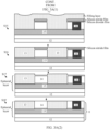
- S10 Form a base 11, as shown in FIG. 3A(1) .
- a method for forming the base 11 includes the following steps.
- S11 Form an epitaxial layer on a silicon substrate 12, and perform ion implantation on the epitaxial layer, to form a buried collector region 15 and a sinker region (sinker) 16.
- Ion implantation of the buried collector region 15 is completed before an STI opening is formed. Ions may be implanted before formation of the epitaxial layer, and then diffused into the epitaxial layer at a high temperature. Alternatively, ion implantation may be performed after the epitaxial layer is formed, to form the buried collector region 15. An order of forming the buried collector region 15 is merely an example. This is not limited.
- a screen oxide (screen oxide) layer may be formed before the buried collector region 15 and the sinker region 16 are formed.
- the screen oxide layer can protect a lattice of the silicon substrate 12 from being damaged.
- the screen oxide layer may be removed, and then subsequent steps are performed.
- no epitaxial layer may alternatively be formed on the silicon substrate 12.
- the buried collector region 15 and the sinker region 16 are located in the silicon substrate 12. This embodiment of this application is described by using an example in which the epitaxial layer is formed on the silicon substrate 12.
- S12 Form a silicon dioxide (SiO2) film and a silicon nitride (Si3N4) film on the epitaxial layer.
- S13 Form the shallow trench isolation (shallow trench isolation, STI) opening in the epitaxial layer.
- the STI opening is formed through photolithography and dry etching. Certainly, another process may alternatively be used. S14: Oxidize and repair a surface of the STI opening, to form a silicon dioxide interface.
- S15 Fill the STI opening with a dielectric material, to form a filling layer.
- the dielectric material is, for example, SiO2 or another field-effect oxide.
- the dielectric material may or may not cover the Si3N4 film, but the STI opening needs to be fully filled with the dielectric material.
- S16 Process the filling layer to form a shallow trench isolation (shallow trench isolation, STI) region 13.
- shallow trench isolation shallow trench isolation, STI
- the filling layer may be ground through a chemical mechanical polishing (chemical mechanical polishing, CMP) process, to stay at a Si3N4 film layer.
- CMP chemical mechanical polishing
- the Si3N4 film may be removed through wet etching.
- a region filled with the SiO2 in the epitaxial layer is the STI region 13, and a remaining region is an active region 14 of the base 11.
- step S17 preparation of the base 11 is basically completed, and then S18' may be performed, to remove a redundant SiO2 film and expose a silicon surface of the base 11.
- the base 11 includes the silicon substrate 12 and the epitaxial layer disposed on the silicon substrate 12.
- the epitaxial layer is divided into the STI region 13, the active region 14, the buried collector region 15, and the sinker region 16. Both the sinker region 16 and the STI region 13 are located on the buried collector region 15.
- the sinker region 16 is in contact with the buried collector region 15.
- the step of forming a base 11 further includes: forming an auxiliary extrinsic base region 21 in the STI region 13.
- the forming the auxiliary extrinsic base region 21 in the STI region 13 includes the following steps. S18: Form a groove below the to-be-formed extrinsic base region in the STI region 13.
- the groove is formed in the STI region 13 through photolithography and dry etching.
- the polycrystalline silicon film may be formed through an epitaxy growth process, or the polycrystalline silicon film may be formed through a chemical vapor deposition (chemical vapor deposition, CVD) process.
- CVD chemical vapor deposition
- a material of the polycrystalline silicon film may be polycrystalline silicon, polycrystalline silicon silicide, or the like.
- doping may be performed on the polycrystalline silicon film. In-situ doping may be performed on the polycrystalline silicon film.
- the polycrystalline silicon film may be formed, and then ion implantation is performed to implement doping.
- S19-2 Pattern the polycrystalline silicon film, and remove the redundant SiO2 film on the surface of the base 11, to form the auxiliary extrinsic base region 17 located in the groove in the STI region 13.
- the SiO2 film may function as a barrier layer, and the polycrystalline silicon film is ground through the CMP process, to remove the polycrystalline silicon film located outside the groove.
- the redundant SiO2 film may be removed through wet etching or dry etching.
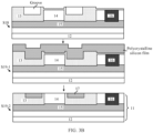
- a surface of the auxiliary extrinsic base region 17 is higher than a surface of the STI region 13. In some other embodiments, as shown in FIG. 3B , a surface of the auxiliary extrinsic base region 17 is flush with a surface of the STI region 13.
- the base 11 may be ground through the CMP process, so that the surface of the auxiliary extrinsic base region 17 is flush with the surface of the STI region 13. In visual effect, this is equivalent to burying the auxiliary extrinsic base region 17 in the STI region 13.
- a height difference within a process error range falls within the protection scope of this embodiment of this application.
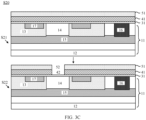
- S20 Form an emitter region window, as shown in FIG. 3C .
- a manner of forming the emitter region window includes the following steps.
- S21 Form a first sacrificial film 31, a second sacrificial film 41, and an auxiliary film 51 that are sequentially stacked on the surface of the base 11, as shown in FIG. 3C .
- Materials of the first sacrificial film 31 and the auxiliary film 51 are the same, and materials of the first sacrificial film 31 and the second sacrificial film 41 are different.
- materials of the first sacrificial film 31, the second sacrificial film 41, and the auxiliary film 51 may all be, for example, silicide.
- materials of the first sacrificial film 31 and the auxiliary film 51 are silicon-containing oxides.
- materials of the first sacrificial film 31 and the auxiliary film 51 are SiO2, silicon oxynitride, or oxygen-rich silicon dioxides.
- a material of the second sacrificial film 41 is silicon-containing nitride.
- a material of the second sacrificial film 41 is Si3N4.
- a manner of forming the first sacrificial film 31, the second sacrificial film 41, and the auxiliary film 51 may be, for example, forming the first sacrificial film 31, the second sacrificial film 41, and the auxiliary film 51 through the chemical vapor deposition (chemical vapor deposition, CVD) process.
- CVD chemical vapor deposition
- S22 Form a third opening 52 in the auxiliary film 51, and form a second opening 42 in the second sacrificial film 41, as shown in FIG. 3C .
- the third opening 52 may be formed in the auxiliary film 51 through photolithography and etching processes.
- the second opening 42 may be formed in the second sacrificial film 41 through the photolithography and etching processes.
- the third opening 52 and the second opening 42 may be formed in two processes, or may be formed in a same process. This is not limited in this embodiment of this application.
- the formed second opening 42 is in communication with the third opening 52 to function as the emitter region window.
- the first sacrificial film 31 is still reserved at a bottom of the emitter region window, and is not directly connected to the base 11.
- the second opening 42 and the third opening 52 are aligned with each other and have a same size.
- an orthographic projection of the second opening 42 on the base 11 coincides with an orthographic projection of the third opening 52 on the base 11.
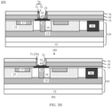
- S30 Form a first inner side wall 60, as shown in FIG. 3D .
- the formed first inner side wall 60 is disposed around a surface that is of the second sacrificial film 41 and that faces the second opening 42 (the emitter region window).
- the formed first inner side wall 60 further extends to a surface that is of the auxiliary film 51 and that faces the third opening 52.
- a manner of forming the first inner side wall 60 includes the following steps.
- S31 Form a first dielectric film 61 on a surface of the auxiliary film 51, where the first dielectric film 61 forms a groove U at the emitter region window, as shown in FIG. 3D .
- a material of the first dielectric film 61 may be a dielectric material, and a material of the first dielectric film 61 is, for example, silicide.
- the material of the first dielectric film 61 is SiO2, Si3N4, silicon oxynitride, or oxygen-rich silicon dioxide.
- the material of the first dielectric film 61 is different from the material of the second sacrificial film 41.
- the material of the first dielectric film 61 is SiO2
- the material of the second sacrificial film 41 is Si3N4.
- a manner of forming the first dielectric film 61 may be, for example, forming the first dielectric film 61 through the CVD process.
- S32 Form a second dielectric film 62 on the first dielectric film 61, as shown in FIG. 3D .
- a manner of forming the second dielectric film 62 may be, for example, forming the second dielectric film 62 through the CVD process.
- a material of the second dielectric film 62 may be a dielectric material, and a material of the second dielectric film 62 is, for example, silicide.
- the material of the second dielectric film 62 is SiO2, Si3N4, silicon oxynitride, or oxygen-rich silicon dioxide.
- the material of the first dielectric film 61 is different from the material of the second dielectric film 62.
- the material of the first dielectric film 61 is SiO2
- the material of the second dielectric film 62 is Si3N4.
- the material of the second sacrificial film 41 is Si3N4
- the material of the first dielectric film 61 is SiO2
- the material of the second dielectric film 62 is Si3N4.
- the first dielectric film 61 blocks a side surface of the second sacrificial film 41, to prevent damage to the second sacrificial film 41 when the second dielectric film 62 is patterned.
- S33 Pattern the second dielectric film 62, to form a second inner wall body 63, where the second inner wall body 63 covers a side surface of the groove U, as shown in FIG. 3D .
- the second dielectric film 62 may be patterned through a dry etching process, to form the second inner wall body 63.
- the first dielectric film 61 may be patterned through a dry etching process, to form the first inner wall body 64.
- the first inner side wall 60 of the semiconductor structure includes the first inner wall body 64 and the second inner wall body 63.
- the first inner side wall 60 exposes the first sacrificial film 31.
- step S34 may not be performed, and when a collector region 18 is subsequently formed, the first dielectric film 61 and the first sacrificial film 31 jointly function as the screen oxide layer.
- S40 Form the collector region 18, where the collector region 18 is located in the active region 14 below the emitter region window, as shown in FIG. 3E .
- step S40 preparation of the substrate 10 of the semiconductor structure is completed.
- the collector region 18 is located in a region enclosed by the STI region 13, and the collector region 18 is in contact with the buried collector region 15.
- the emitter region window functions as a self-aligned window
- the first sacrificial film 31 functions as the screen oxide (screen oxide) layer
- an ion implantation process is used in selective implantation (selected implanted), to form the collector (collector) region 18.
- the screen oxide layer can protect a lattice of the base 11 from being damaged, and the prepared collector region 18 is well directly aligned with the emitter region window.
- S50 Form a first opening 32 in the first sacrificial film 31, where the first opening 32 is in communication with the second opening 42, as shown in FIG. 3F .
- the first sacrificial film 31 located under the second opening 42 is removed through wet etching, to form the first opening 32. Because wet etching is isotropic, if materials of the first inner wall body 64 and the first sacrificial film 31 are the same (for example, are both SiO2), in a process of forming the first opening 32, the first inner wall body 64 located under the second inner wall body 63 is also removed.
- an etching amount of the first sacrificial film 31 may be controlled by controlling an etching time period.
- a size of the first opening 32 may be controlled by controlling the etching time period.
- a contour of the second opening 42 is within a contour of the first opening 32.
- an orthographic projection of the second opening 42 on the substrate 10 is within an orthographic projection of the first opening 32 on the substrate 10.
- the first opening 32 is larger than the second opening 42, and there is a hole under the second sacrificial film 41.
- S60 Form the intrinsic base region 21 in the first opening 32, as shown in FIG. 3G .
- the intrinsic base region 21 may be selectively epitaxially grown on the surface of the substrate 10 through a selective epitaxy growth process.
- a material of the intrinsic base region 21 may include, for example, SiGe (silicon germanium) and SiGe:C (silicon-germanium-carbon) alloy.
- the hole is filled with the intrinsic base region 21.
- S70 Remove the first inner side wall 60, to form a second inner side wall 70, as shown in FIG. 3H .
- the formed second inner side wall 70 includes a third inner wall body 71 and a fourth inner wall body 72.
- the third inner wall body 71 is disposed around both a surface that is of the second sacrificial film 41 and that faces the second opening 42 and a surface that is of the auxiliary film 51 and that faces the third opening 52.
- the third inner wall body 71 is L-shaped.
- the fourth inner wall body 72 is disposed on the third inner wall body 71, and is not directly in contact with the intrinsic base region 21.
- materials of the third inner wall body 71 and the first inner wall body 64 are the same.
- a material of the third inner wall body 71 is SiO2.
- Materials of the fourth inner wall body 72 and the second inner wall body 63 are the same.
- a material of the fourth inner wall body 72 is Si3N4.
- the formed second inner side wall 70 includes the third inner wall body 71.
- a step of removing the fourth inner wall body 72 is further included.
- the second inner side wall 70 includes only a single-layer inner wall body, an opening of the emitter region window is relatively large, and the finally formed emitter region has a large area and small resistance.
- step S40 is performed, and when ion implantation is performed to form the collector region 18, ion implantation is performed on the first inner side wall 60, affecting isolation effect between the extrinsic base region and the emitter region that are subsequently formed. Therefore, after the first inner side wall 60 is removed and the second inner side wall 70 is formed again, the foregoing problem can be resolved, and the isolation effect between the extrinsic base region and the emitter region can be improved.
- a part that is of the first inner wall body 64 and that is in contact with the first sacrificial film 31 is removed synchronously, that is, a cross section of the first inner wall body 64 is strip-shaped.
- a third inner wall body 71 included in the second inner wall body 70 that is formed again is L-shaped and has a wide coverage area, so that isolation effect between the extrinsic base region and the emitter region can be improved.
- the surface of the intrinsic base region 21 may be cleaned through wet etching, to remove an intrinsic oxidized layer generated after the surface of the intrinsic base region 21 is oxidized.
- step S70 is further performed.
- an exposed surface of the intrinsic base region 21 is prone to oxidation to produce SiO2, which affects electrical contact effect between the subsequently formed emitter region and the subsequently intrinsic base region 21, leading to higher resistance in the emitter region.
- the surface of the intrinsic base region 21 is cleaned, so that SiO2 on the surface of the intrinsic base region 21 can be removed. This improves the electrical contact effect between the subsequently formed emitter region and the subsequently intrinsic base region 21, facilitates epitaxy growth of a single crystal material in the emitter region, and effectively reduces resistance of the emitter region.
- S90 Form, at the emitter region window, an emitter region film 81 that is in contact with the intrinsic base region 21, and pattern the emitter region film 81 and the auxiliary film 51, to form an emitter region 80 and an auxiliary layer 50, as shown in FIG. 3I .
- a material of the emitter region 80 may be, for example, doped epitaxial monocrystalline silicon or polycrystalline silicon, or in-situ doping may be performed on the emitter region 80, to enhance doping concentration.
- the semiconductor structure does not include a cap layer, or a cap layer is not formed synchronously with the emitter region 80.
- the forming the emitter region 80 includes: forming the emitter region film 81, where the emitter region film 81 covers the auxiliary film 51 and the second inner side wall 70. Then, the emitter region film 81 is patterned, to form the emitter region 80.
- the auxiliary film 51 is patterned synchronously (a part that is of the auxiliary film 51 and that is not covered by the emitter region 80 is removed). In other words, the emitter region 80 and the auxiliary layer 50 are formed synchronously.
- the auxiliary film 51 may be patterned through photolithography and dry etching processes, to form the auxiliary layer 50.
- the emitter region 80 and a cap layer 90 are formed synchronously.
- the forming the emitter region 80 includes the following steps.
- the emitter region film 81 may be formed through the epitaxy growth process.
- a material of the emitter region film 81 may be, for example, doped epitaxial monocrystalline silicon or polycrystalline silicon.
- a material of the cap film 91 may be a dielectric material, and a material of the cap film 91 is, for example, silicide.
- the material of the cap film 91 is silicon oxide, silicon nitride, silicon oxynitride, or oxygen-rich silicon dioxide.
- the cap film 91 may be formed through the CVD process, and the cap film 91 covers the emitter region film 81.
- S93 Pattern a film (for example, the auxiliary film 51, the emitter region film 81, and the cap film 91) on a side that is of the second sacrificial film 41 and that is away from the substrate 10, to form the auxiliary layer 50, the emitter region 80, and the cap layer 90.
- a film for example, the auxiliary film 51, the emitter region film 81, and the cap film 91
- the auxiliary film 51, the emitter region film 81, and the cap film 91 are patterned through the photolithography and etching processes, to expose the second sacrificial film 41.
- the patterning of the auxiliary film 51, the emitter region film 81, and the cap film 91 may be completed in a plurality of processes, or may be completed in a same process. Specific patterns of structures retained after the auxiliary film 51, the emitter region film 81, and the cap film 91 are patterned are not limited, provided that the patterns are appropriately set based on a requirement.
- S100 Form a first outer wall body 103 and a second outer wall body 104, as shown in FIG. 3J .
- the first outer wall body 103 is disposed between the second outer wall body 104 and the emitter region 80.
- the first outer wall body 103 and the second outer wall body 104 wrap at least a side surface of the emitter region 80.
- the first outer wall body 103 and the second outer wall body 104 wrap side surfaces of the auxiliary layer 50, the emitter region 80, and the cap layer 90.
- a method for forming the first outer wall body 103 and the second outer wall body 104 includes the following steps.
- S 101 Form a third dielectric film 101 on the substrate 10 on which the cap layer 90 is formed.
- a manner of forming the third dielectric film 101 may be, for example, forming the third dielectric film 101 through the CVD process.
- a material of the third dielectric film 101 may be a dielectric material, and a material of the third dielectric film 101 is, for example, silicide.
- the material of the third dielectric film 101 is SiO2, Si3N4, silicon oxynitride, or oxygen-rich silicon dioxide.
- the material of the third dielectric film 101 is different from a material of the first sacrificial film 31.
- the material of the third dielectric film 101 is Si3N4, and the material of the first sacrificial film 31 is SiO2.
- the first outer side wall 103 formed by the third dielectric film 101 is not removed, to ensure that the outer side wall protects the emitter region 21.
- S102 Form a fourth dielectric film 102 on the third dielectric film 101.
- a manner of forming the fourth dielectric film 102 may be, for example, forming the fourth dielectric film 102 through the CVD process.
- a material of the fourth dielectric film 102 may be a dielectric material, and the material of the fourth dielectric film 102 is, for example, silicide.
- the material of the fourth dielectric film 102 is SiO2, Si3N4, silicon oxynitride, or oxygen-rich silicon dioxide.
- the material of the fourth dielectric film 102 is different from the material of the second sacrificial film 41.
- the material of the fourth dielectric film 102 is SiO2
- the material of the second sacrificial film 41 is Si3N4.
- the third dielectric film 101 and the fourth dielectric film 102 may be patterned through the etching process, to form the first outer wall body 103 and the second outer wall body 104.
- a process of patterning the third dielectric film 101 and the fourth dielectric film 102 may be completed in a same process, or may be separately completed in a plurality of processes.
- a method for forming the extrinsic base region 22 includes the following steps.
- the second sacrificial film 41 may be removed through the etching process. Two ends of the intrinsic base region 21 are exposed to function as a seed crystal for forming a baselink region 221.
- S112 Form the baselink region 221 under the auxiliary layer 50.
- the baselink region 221 may be formed through the selective epitaxy growth process.
- a size of the baselink region 221 is not limited in this embodiment of this application, provided that the baselink region 221 is in contact with the intrinsic base region 21.
- a structure of the baselink region 221 shown in FIG. 3K(1) and FIG. 3K(2) is merely an example, and is not limited.
- a material of the baselink region 221 may include, for example, heavily doped monocrystalline silicon, and may further include a small quantity of polycrystalline silicon.
- the first sacrificial film 31 may be removed through the etching process.
- the surface of the substrate 10 is exposed, and the auxiliary extrinsic base region 17 is exposed.
- the reserved first outer wall body 103 functions as an outer side wall 100 of the semiconductor structure, and the outer side wall 100 is configured to protect the emitter region 80.
- the extrinsic base region film 222 may be formed at the corresponding position of the first sacrificial film 31 through the selective epitaxy growth process.
- the extrinsic base region film 222 is formed on the surface of the substrate 10, and the extrinsic base region film 222 is in direct contact with the auxiliary extrinsic base region 17.
- a material of the extrinsic base region film 222 may be, for example, polycrystalline silicon or polycrystalline silicon silicide. In some embodiments, in-situ doping may be further performed on the extrinsic base region film 222.
- the formed extrinsic base region film 222 may be in contact with the intrinsic base region 21, or may not be in contact with the intrinsic base region 21.
- an effective extrinsic base region 223 formed by using the extrinsic base region film 222 may be in contact with the intrinsic base region 21, or may not be in contact with the intrinsic base region 21.
- the extrinsic base region film 222 may be patterned through the photolithography and etching processes.
- a method for forming the extrinsic base region 22 includes: The auxiliary extrinsic base region 17 further functions as a seed layer of the extrinsic base region film 222, and directly epitaxially grows the extrinsic base region 22 on the auxiliary extrinsic base region 17.
- the sinker region 16 is covered with a dielectric protection layer, to ensure that the extrinsic base region 22 epitaxially grows only on the auxiliary extrinsic base region 17, and a structure in S115 is directly obtained. This saves patterning steps, such as photolithography and etching, performed on the extrinsic base region.
- the extrinsic base region 22 formed by using the foregoing method includes the effective extrinsic base region 223 and the baselink region 221.
- the effective extrinsic base region 223 is in contact with the baselink region 221, and the baselink region 221 is in contact with the intrinsic base region 21, so that the extrinsic base region 22 is in contact with the intrinsic base region 21.
- the material of the baselink region 221 is quasi-single-crystalline silicon, and an activation rate of a doping ion of the baselink region 221 is greater than that of the effective extrinsic base region 223 (a material is polycrystalline silicon). Therefore, the contact between the effective extrinsic base region 223 and the intrinsic base region 21 is implemented through the baselink region 221, so that contact resistance between the extrinsic base region 22 and the intrinsic base region 21 can be reduced.
- the effective extrinsic base region 223 is in contact with the auxiliary extrinsic base region 17 on the surface of the substrate 10.
- the effective extrinsic base region 223 is in contact with the auxiliary extrinsic base region 17, which is equivalent to increasing a thickness of the effective extrinsic base region 223. This may raise the extrinsic base region 22, to reduce resistance of the extrinsic base region 22.
- a method for forming the extrinsic base region 22 includes the following steps.
- a process of removing the second sacrificial film 41 and a process of removing the first sacrificial film 31 may be completed in a same process, or may be completed in different processes.
- S113' Form the extrinsic base region film 222 at corresponding positions of the first sacrificial film 31 and the second sacrificial film 41.
- the formed extrinsic base region 22 is directly linked to the intrinsic base region 21, and the extrinsic base region 22 is in contact with the auxiliary extrinsic base region 17 on the surface of the substrate 10, so that the extrinsic base region 22 may be raised, to reduce the resistance of the extrinsic base region 22.
- S120 Perform heat treatment on the semiconductor structure.
- Heat treatment for example, annealing
- annealing is performed on a structure obtained in FIG. 3K(2) or FIG. 3L , and doping distribution in the emitter region 80, the intrinsic base region 21, the extrinsic base region 22, and the collector region 18 is adjusted, to activate doping ions.
- the emitter electrode E is in contact with the emitter region 80 through a connection hole (contact) 110 provided in a surface of the emitter region 80.
- the base electrode B is in contact with the extrinsic base region 22 through a connection hole 110 in a surface of the extrinsic base region 22.
- the sinker region 16 is in contact with the collector region 18 through the buried collector region 15, and the collector electrode C is in contact with the sinker region 16 through a connection hole 110 provided in a surface of the sinker region 16, so that the collector electrode C is in contact with the collector region 18.
- connection hole 100 passes through the dielectric layer and is in contact with the emitter region 80, the extrinsic base region, and the sinker region 16.
- preparation method for the semiconductor structure provided in this embodiment of this application is not limited to the foregoing steps, and another step may be added or some of the foregoing steps may be removed as required.
- an order of the steps in the foregoing preparation method is merely an example, and may be adjusted based on a requirement.
- the semiconductor structure obtained by using the foregoing steps S10 to S130 is an HBT device.
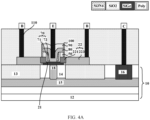
- the semiconductor structure includes: the substrate 10, including the shallow trench isolation region 13 and the active region 14.
- the active region 14 includes the buried collector region 15, the sinker region 16, and the collector region 18.
- the collector region 18 is buried in the substrate 10, and a surface of the collector region 18 is flush with the surface of the substrate 10.
- the collector region 18 is located in the active region 14 under the intrinsic base region 21.
- the shallow trench isolation region 13 is disposed at a periphery of the active region 14 under the intrinsic base region 21.
- the sinker region 16 is located on a side that is of the shallow trench isolation region 13 and that is away from the collector region 18.
- the sinker region 16 and the shallow trench isolation region 13 are located on the buried collector region 15. Both the sinker region 16 and the collector region 18 are in contact with the buried collector region 15.
- the substrate 10 further includes the auxiliary extrinsic base region 17.
- the auxiliary extrinsic base region 17 is disposed in the shallow trench isolation region 13, and the surface of the auxiliary extrinsic base region 17 functions as a part of the surface of the substrate 10.
- the intrinsic base region 21 is disposed on the surface of the substrate 10, is in contact with the collector region 18 on the surface of the substrate 10, and forms a collector junction (C-B).
- the material of the intrinsic base region 21 may be, for example, SiGe or SiGe:C.
- the extrinsic base region 22 is disposed on the surface of the substrate 10, and is in contact with the auxiliary extrinsic base region 17 on the surface of the substrate 10.
- the extrinsic base region 22 is located at a periphery of the intrinsic base region 21, and is in contact with the intrinsic base region 21.
- a material of the extrinsic base region 22 may be, for example, polycrystalline silicon.
- step S111 to step S115 are performed, to form the extrinsic base region 22.
- the extrinsic base region 22 includes the baselink region 221 and the effective extrinsic base region 223, and the baselink region 221 is in contact with both the intrinsic base region 21 and the effective extrinsic base region 223.
- the baselink region 221 is linked to the intrinsic base region 21, and the baselink region 221 is linked to the effective extrinsic base region 223.
- the baselink region 221 is disposed on the intrinsic base region 21, and the baselink region 221 is spliced with the effective extrinsic base region 223.
- the baselink region 221 is in contact with both the intrinsic base region 21 and the effective extrinsic base region 223 in different manners.
- the foregoing is merely an example, and is not limited.
- the effective extrinsic base region 223 may not be in contact with the intrinsic base region 21. As shown in FIG. 4B , the effective extrinsic base region 223 may alternatively be in contact with the intrinsic base region 21.
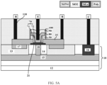
- step S111' to step S114' are performed, to form the extrinsic base region 22.
- the extrinsic base region 22 does not include the baselink region, and materials of all parts of the extrinsic base region 22 are the same.
- the auxiliary layer 50 has an opening, and the auxiliary layer 50 is disposed on the extrinsic base region 22.
- the opening in the auxiliary layer 50 may be understood as the third opening 52 in the auxiliary film 51 in the foregoing preparation process.
- a material of the auxiliary layer 50 may be, for example, SiO2.
- the emitter region 80 is disposed on the auxiliary layer 50, and is in contact with the intrinsic base region 21 through the opening, to form an emitter junction (E-B).
- the material of the emitter region 80 may be, for example, doped epitaxial monocrystalline silicon or polycrystalline silicon.
- An inner side wall is disposed between the extrinsic base region 22 and the emitter region 80, may further extend between the auxiliary layer 50 and the emitter region 80, and is configured to isolate the extrinsic base region 22 from the emitter region 80.
- step S70 is performed in the preparation process of the semiconductor structure.
- the inner side wall in the semiconductor structure may be the second inner side wall 70.
- the second inner side wall 70 may include the third inner wall body 71 and the fourth inner wall body 72.
- the second inner wall body 70 may alternatively include only the third inner wall body 71.
- the inner side wall includes an L-shaped part (the third inner wall body 71).
- a material of the third inner wall body 71 may be, for example, SiO2
- a material of the fourth inner wall body 72 may be, for example, Si3N4.
- step S70 is not performed in the preparation process of the semiconductor structure.
- the inner side wall in the semiconductor structure may be the first inner side wall 60.
- the first inner side wall 60 may include the first inner wall body 64 and the second inner wall body 63.
- the first inner side wall 60 may alternatively include only the first inner wall body 64.
- a material of the first inner wall body 64 may be, for example, SiO2
- a material of the second inner wall body 63 may be, for example, Si3N4.
- the cap layer 90 covers a surface that is of the emitter region 80 and that is away from the substrate 10, and is configured to protect the emitter region 80.
- a material of the cap layer 90 may be, for example, SiO2.
- the outer side wall 100 wraps a side surface of the emitter region 80, and is configured to protect the emitter region 80.
- the outer side wall 100 may be the first outer wall body 103 in the foregoing preparation process.
- a material of the outer side wall 100 may be, for example, Si3N4.
- the collector electrode C is in contact with the collector region 18 through a connection hole 100 that is in contact with the sinker region 16 through the sinker region 16 and the buried collector region 15.
- the connection hole 100 may be directly provided in the surface of the sinker region 16, and a metal silicide layer may further be disposed between the connection hole 100 and the sinker region 16, to implement contact between the connection hole 100 and the sinker region 16.
- the emitter electrode E is in contact with the emitter region 80 through a connection hole 100 that passes through the cap layer 90 and is in contact with the emitter region 80.
- the connection hole 100 may be directly provided in the surface of the emitter region 80, and a metal silicide layer may further be disposed between the connection hole 100 and the emitter region 80, to implement contact between the connection hole 100 and the emitter region 80.
- the base electrode B is in contact with the extrinsic base region 22 through a connection hole 100 that is in contact with the extrinsic base region 22.
- the connection hole 100 may be directly provided in the surface of the extrinsic base region 22, and a metal silicide layer may further be disposed between the connection hole 100 and the extrinsic base region 22, to implement contact between the connection hole 100 and the extrinsic base region 22.
- connection hole 100 inevitably passes through the dielectric layer.
- the emitter electrode E is configured to emit electrons.
- the base electrode B is configured to control the electrons (so that a current flowing to the collector electrode C is controlled by an input signal of the base electrode B).
- the collector electrode C is configured to collect the electrons.
- a SiGe HBT transistor in the foregoing semiconductor structure may be an NPN transistor (the intrinsic base region 21 is a P region, that is, the semiconductor is a P-type semiconductor; both the emitter region 80 and the collector region 18 are N regions, that is, the semiconductor is an N-type semiconductor), or a PNP transistor (the intrinsic base region 21 is an N region, that is, the semiconductor is an N-type semiconductor; both the emitter region 80 and the collector region 18 are P regions, that is, the semiconductor is a P-type semiconductor).
- emitter electrode E structures, positions, and quantities of the emitter electrode E, the base electrode B, and the collector electrode C that are shown in the schematic diagrams of embodiments of this application are merely examples. There may be only one emitter electrode E, one base electrode B, and one collector electrode C. Alternatively, there may be one base electrode B and one collector electrode C on a left side of the emitter electrode E, and one base electrode B and one collector electrode C on a right side of the emitter electrode E.
- a material of the film layer in FIG. 3M is merely an example, and is not limited.
- the NPN HBT device is used as an example to describe a working principle of the SiGe HBT device provided in this embodiment of this application.
- a power supply is applied to the emitter junction, the emitter junction is positively biased, and majority carriers (free electrons) in the emitter region 80 continuously cross the emitter junction and enter the intrinsic base region 21, to form an emitter current.
- the electrons After entering the intrinsic base region 21, the electrons first accumulate near the emitter junction, and gradually form an electron concentration difference. Under effect of the concentration difference, an electron flow is driven to diffuse toward the collector junction in the intrinsic base region 21, and is pulled into the collector region 18 by an electric field of the collector junction, to form a collector current.
- a small part of electrons (because the intrinsic base region 21 is extremely thin) are combined with holes in the intrinsic base region 21, and a ratio of a diffused electron flow to a combined electron flow determines an amplification capability of a triode. Due to a large reverse voltage applied to the collector junction, an electric field force generated by this reverse voltage prevents electrons in the collector region 18 from diffusing into the intrinsic base region 21, and pulls electrons that are diffused near the collector junction into the collector region 18, to form a main collector current. In addition, minority carriers (holes) in the collector region 18 also perform drift motion, and flow toward the intrinsic base region 21, to form a reverse saturation current.
- the first sacrificial film 31, the second sacrificial film 41, and the auxiliary film 51 function as self-aligned structures, and may be used to implement self-alignment of the collector junction (C-B) and self-alignment of the emitter junction (E-B).
- the collector junction and the emitter junction that are obtained through preparation are axisymmetric structures, and no deviations occur in photolithography and etching processes, preventing asymmetry in both the collector junction and the emitter junction.
- the emitter junction is asymmetric.
- parasitic collector junction capacitance and base region resistance on two sides of the emitter junction are different, a current cannot be evenly distributed on the two sides, and total resistance and capacitance cannot be minimized.
- the two sides are symmetric, so that the base region resistance and the collector junction capacitance can be minimized, and a maximum oscillation frequency of the device is increased.
- the collector junction is asymmetric.
- parasitic collector resistance on two sides of the collector junction is different, and an objective of reducing the collector resistance cannot be implemented either.
- preparation of each film layer may be implemented by using a conventional technology.
- the collector region 18 is also formed by defining a position by using the self-aligned structure and then performing ion implantation on the substrate 10.
- both the intrinsic base region 21 and the extrinsic base region 22 are disposed on the surface of the substrate 10, and the collector region 18 is disposed inside the substrate 10. There is no raised epitaxial collector region. Therefore, both the intrinsic base region 21 and the extrinsic base region 22 are directly formed on the surface of the known substrate 10, and whether the intrinsic base region 21 is in contact with the extrinsic base region 22 is directly controlled by preparation processes of the intrinsic base region and the extrinsic base region. Compared with the intrinsic base region disposed on the epitaxial collector region that is disposed on the surface of the substrate 10, the intrinsic base region 21 is directly disposed on the surface of the substrate 10 in this embodiment of this application.
- contact between the intrinsic base region 21 and the extrinsic base region 22 is not affected due to a parameter like a thickness of the raised epitaxial collector region.
- This can improve a contact yield between the intrinsic base region 21 and the extrinsic base region 22, and further improve a yield of the semiconductor structure.
- impact of the thickness of the collector region 18 on contact effect between the intrinsic base region 21 and the extrinsic base region 22 does not need to be considered. Therefore, this can reduce a requirement for process accuracy of manufacturing the collector region 18, and reduce a process difficulty.
- the collector region 18 is obtained through doping, and an epitaxy growth process (for preparing the collector region 18) is not needed. This saves processing costs.
- an auxiliary extrinsic base region 17 is disposed in the substrate 10, and the auxiliary extrinsic base region 17 functions as a seed layer for epitaxy growth of the extrinsic base region 22. After the extrinsic base region 22 is grown, the auxiliary extrinsic base region 17 is in contact with the extrinsic base region 22, to implement thickening of the extrinsic base region 22. This can implement an objective of reducing resistance of the extrinsic base region.
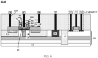
- the semiconductor structure further includes a complementary metal-oxide-semiconductor field-effect transistor (complementary metal oxide semiconductor field-effect transistor, CMOSFET).
- the preparation method for the semiconductor structure further includes: S140, that is, forming the CMOSFET on the base 11.
- the step of forming the CMOSFET on the base 11 may be performed before step S10, or may be performed after step S130.
- a SiGe HBT structure and the CMOSFET structure are isolated from each other through a deep trench isolation region 19 in the substrate 10.
- the CMOSFET structure is not limited in this embodiment of this application, and the CMOSFET in FIG. 6 is merely an example.
- the CMOSFET may be an NMOS transistor or a PMOS transistor.
- the semiconductor structure obtained through preparation by using the preparation method for the semiconductor structure is a CMOS+SiGe HBT device, and the CMOS and the SiGe HBT may be integrated on a same chip.
- the transistor circuit may be directly packaged by using a package body, to form a packaged component (for example, a chip), or may be packaged together with another chip, to form a packaged component. This is not limited in this embodiment of this application.
- the transistor circuit including any one of the foregoing semiconductor structures may be used in a radio frequency circuit.
- the radio frequency circuit may be used in fields, for example, a microwave system, an optoelectronic system, radar, image, and sensing.
- the radio frequency circuit may be, for example, a power amplifier (power amplifier, PA), a variable gain amplifier (variable gain amplifier, VGA), a low noise amplifier (low noise amplifier, LNA), a trans-impedance amplifier (trans-impedance amplifier, TIA), a driver (driver), a frequency mixer, or a clock data recovery (clock data recovery, CDR) circuit.
- the semiconductor structure may be applied to any communication apparatus.
- the communication apparatus may be a network device, or may be a terminal.
Landscapes
- Bipolar Transistors (AREA)
Applications Claiming Priority (1)
| Application Number | Priority Date | Filing Date | Title |
|---|---|---|---|
| PCT/CN2021/117293 WO2023035155A1 (zh) | 2021-09-08 | 2021-09-08 | 半导体结构及其制备方法、射频电路 |
Publications (2)
| Publication Number | Publication Date |
|---|---|
| EP4391027A1 true EP4391027A1 (de) | 2024-06-26 |
| EP4391027A4 EP4391027A4 (de) | 2024-10-09 |
Family
ID=85507108
Family Applications (1)
| Application Number | Title | Priority Date | Filing Date |
|---|---|---|---|
| EP21956343.4A Pending EP4391027A4 (de) | 2021-09-08 | 2021-09-08 | Halbleiterstruktur und herstellungsverfahren dafür sowie hochfrequenzschaltung |
Country Status (3)
| Country | Link |
|---|---|
| EP (1) | EP4391027A4 (de) |
| CN (1) | CN117941040A (de) |
| WO (1) | WO2023035155A1 (de) |
Cited By (1)
| Publication number | Priority date | Publication date | Assignee | Title |
|---|---|---|---|---|
| EP4425536A4 (de) * | 2021-11-18 | 2024-11-27 | Huawei Technologies Co., Ltd. | Halbleiterstruktur und herstellungsverfahren dafür sowie hochfrequenzschaltung und kommunikationsvorrichtung |
Family Cites Families (10)
| Publication number | Priority date | Publication date | Assignee | Title |
|---|---|---|---|---|
| CN101359682B (zh) * | 2008-09-12 | 2012-02-08 | 清华大学 | 自对准抬升外基区双极晶体管及其制备方法 |
| DE102009001552A1 (de) * | 2008-12-12 | 2010-06-17 | Ihp Gmbh - Innovations For High Performance Microelectronics / Leibniz-Institut Für Innovative Mikroelektronik | Bipolartransistor mit selbstjustiertem Emitterkontakt |
| CN102130152B (zh) * | 2010-01-18 | 2014-12-10 | 上海华虹宏力半导体制造有限公司 | 自对准双极晶体管及其制作方法 |
| EP2506297A1 (de) * | 2011-03-29 | 2012-10-03 | Nxp B.V. | Bi-CMOS-Vorrichtung und Verfahren |
| CN103022110B (zh) * | 2012-12-20 | 2015-07-29 | 清华大学 | 金属硅化物抬升外基区全自对准双极晶体管及其制备方法 |
| FR3047838A1 (fr) * | 2016-02-16 | 2017-08-18 | St Microelectronics Sa | Transistor bipolaire et son procede de fabrication |
| EP3547371B1 (de) * | 2018-03-27 | 2025-10-15 | NXP USA, Inc. | Bipolartransistor und verfahren zur herstellung eines bipolartransistors |
| US10777668B2 (en) * | 2018-08-21 | 2020-09-15 | Globalfoundries Inc. | Bipolar junction transistors with a self-aligned emitter and base |
| US11018247B1 (en) * | 2019-12-26 | 2021-05-25 | Nxp Usa, Inc. | Semiconductor device with a base link region and method therefor |
| CN111883580B (zh) * | 2020-06-23 | 2022-12-20 | 西安理工大学 | 一种浅沟槽场板SiGe HBT及其制作方法 |
-
2021
- 2021-09-08 CN CN202180102025.0A patent/CN117941040A/zh active Pending
- 2021-09-08 WO PCT/CN2021/117293 patent/WO2023035155A1/zh not_active Ceased
- 2021-09-08 EP EP21956343.4A patent/EP4391027A4/de active Pending
Cited By (1)
| Publication number | Priority date | Publication date | Assignee | Title |
|---|---|---|---|---|
| EP4425536A4 (de) * | 2021-11-18 | 2024-11-27 | Huawei Technologies Co., Ltd. | Halbleiterstruktur und herstellungsverfahren dafür sowie hochfrequenzschaltung und kommunikationsvorrichtung |
Also Published As
| Publication number | Publication date |
|---|---|
| EP4391027A4 (de) | 2024-10-09 |
| WO2023035155A1 (zh) | 2023-03-16 |
| CN117941040A (zh) | 2024-04-26 |
Similar Documents
| Publication | Publication Date | Title |
|---|---|---|
| JP3701873B2 (ja) | ヘテロ接合バイポーラ・トランジスタの作製方法 | |
| CN105321995B (zh) | 双极晶体管结构和制造双极晶体管结构的方法 | |
| EP2076919B1 (de) | Verfahren zur Herstellung lokaler Kollektorimplantationsstruktur für Heteroübergangsbipolartransistoren | |
| US7488662B2 (en) | Self-aligned vertical PNP transistor for high performance SiGe CBiCMOS process | |
| US10014397B1 (en) | Bipolar junction transistors with a combined vertical-lateral architecture | |
| KR100554465B1 (ko) | SOI 기판 위에 구현된 SiGe BiCMOS 소자 및그 제조 방법 | |
| EP2919272B1 (de) | Bipolare Transistorvorrichtung und Verfahren zur Herstellung | |
| CN107680966A (zh) | 自对准与非自对准的异质接面双极晶体管的共同整合 | |
| EP3843159A1 (de) | Halbleiterbauelement mit einem basisverbindungsbereich und verfahren dafür | |
| US12062699B2 (en) | Horizontal Current Bipolar Transistor with Silicon-Germanium base | |
| KR100474867B1 (ko) | 반도체장치 및 그 제조방법 | |
| EP1997130B1 (de) | Verfahren zur herstellung eines bipolartransistors | |
| EP4391027A1 (de) | Halbleiterstruktur und herstellungsverfahren dafür sowie hochfrequenzschaltung | |
| Van Huylenbroeck et al. | A 400GHz f MAX fully self-aligned SiGe: C HBT architecture | |
| EP4425536A1 (de) | Halbleiterstruktur und herstellungsverfahren dafür sowie hochfrequenzschaltung und kommunikationsvorrichtung | |
| JP2001196382A (ja) | 半導体装置及びその製造方法 | |
| JP4014548B2 (ja) | 半導体装置及びその製造方法 | |
| CN102412275A (zh) | 锗硅BiCMOS工艺中纵向PNP器件及制作方法 | |
| KR20040038511A (ko) | 자기정렬형 이종접합 쌍극자 트랜지스터 및 그의 제조 방법 | |
| CN114256071B (zh) | 一种异质结双极晶体管及其制造方法 | |
| WO2023044773A1 (zh) | 半导体结构及其制备方法、射频电路、终端 | |
| JPH11233524A (ja) | バイポーラトランジスタ及びその製造方法 | |
| US20130113020A1 (en) | Sige hbt and method of manufacturing the same |
Legal Events
| Date | Code | Title | Description |
|---|---|---|---|
| STAA | Information on the status of an ep patent application or granted ep patent |
Free format text: STATUS: THE INTERNATIONAL PUBLICATION HAS BEEN MADE |
|
| PUAI | Public reference made under article 153(3) epc to a published international application that has entered the european phase |
Free format text: ORIGINAL CODE: 0009012 |
|
| STAA | Information on the status of an ep patent application or granted ep patent |
Free format text: STATUS: REQUEST FOR EXAMINATION WAS MADE |
|
| 17P | Request for examination filed |
Effective date: 20240318 |
|
| AK | Designated contracting states |
Kind code of ref document: A1 Designated state(s): AL AT BE BG CH CY CZ DE DK EE ES FI FR GB GR HR HU IE IS IT LI LT LU LV MC MK MT NL NO PL PT RO RS SE SI SK SM TR |
|
| A4 | Supplementary search report drawn up and despatched |
Effective date: 20240909 |
|
| RIC1 | Information provided on ipc code assigned before grant |
Ipc: H01L 29/10 20060101ALI20240903BHEP Ipc: H01L 29/737 20060101ALI20240903BHEP Ipc: H01L 21/331 20060101AFI20240903BHEP |
|
| DAV | Request for validation of the european patent (deleted) | ||
| DAX | Request for extension of the european patent (deleted) |