EP4391226A1 - Dispositif électronique - Google Patents
Dispositif électronique Download PDFInfo
- Publication number
- EP4391226A1 EP4391226A1 EP22869297.6A EP22869297A EP4391226A1 EP 4391226 A1 EP4391226 A1 EP 4391226A1 EP 22869297 A EP22869297 A EP 22869297A EP 4391226 A1 EP4391226 A1 EP 4391226A1
- Authority
- EP
- European Patent Office
- Prior art keywords
- radiator
- antenna structure
- electronic device
- ground
- side frame
- Prior art date
- Legal status (The legal status is an assumption and is not a legal conclusion. Google has not performed a legal analysis and makes no representation as to the accuracy of the status listed.)
- Pending
Links
- 239000003990 capacitor Substances 0.000 claims description 61
- 229910052751 metal Inorganic materials 0.000 claims description 32
- 239000002184 metal Substances 0.000 claims description 32
- 238000007667 floating Methods 0.000 claims description 6
- 230000005855 radiation Effects 0.000 description 36
- 238000010586 diagram Methods 0.000 description 33
- 230000008878 coupling Effects 0.000 description 24
- 238000010168 coupling process Methods 0.000 description 24
- 238000005859 coupling reaction Methods 0.000 description 24
- 238000004891 communication Methods 0.000 description 20
- 238000009826 distribution Methods 0.000 description 19
- YKKYCYQDUUXNLN-UHFFFAOYSA-N 2,4-dichloro-1-(2-chlorophenyl)benzene Chemical compound ClC1=CC(Cl)=CC=C1C1=CC=CC=C1Cl YKKYCYQDUUXNLN-UHFFFAOYSA-N 0.000 description 11
- 238000005516 engineering process Methods 0.000 description 10
- 238000013461 design Methods 0.000 description 9
- 238000002955 isolation Methods 0.000 description 8
- 239000000463 material Substances 0.000 description 8
- 239000006059 cover glass Substances 0.000 description 7
- RYGMFSIKBFXOCR-UHFFFAOYSA-N Copper Chemical compound [Cu] RYGMFSIKBFXOCR-UHFFFAOYSA-N 0.000 description 6
- 238000009413 insulation Methods 0.000 description 6
- 238000000034 method Methods 0.000 description 6
- 239000004020 conductor Substances 0.000 description 5
- 238000004088 simulation Methods 0.000 description 5
- 230000005540 biological transmission Effects 0.000 description 4
- 230000006870 function Effects 0.000 description 4
- 238000004519 manufacturing process Methods 0.000 description 4
- 229910000831 Steel Inorganic materials 0.000 description 3
- 238000010521 absorption reaction Methods 0.000 description 3
- 230000008859 change Effects 0.000 description 3
- 229910052802 copper Inorganic materials 0.000 description 3
- 239000010949 copper Substances 0.000 description 3
- 239000011889 copper foil Substances 0.000 description 3
- 239000011888 foil Substances 0.000 description 3
- 239000007769 metal material Substances 0.000 description 3
- 229910052755 nonmetal Inorganic materials 0.000 description 3
- 239000004033 plastic Substances 0.000 description 3
- 229920003023 plastic Polymers 0.000 description 3
- 229920000139 polyethylene terephthalate Polymers 0.000 description 3
- 239000005020 polyethylene terephthalate Substances 0.000 description 3
- 239000010959 steel Substances 0.000 description 3
- OKTJSMMVPCPJKN-UHFFFAOYSA-N Carbon Chemical compound [C] OKTJSMMVPCPJKN-UHFFFAOYSA-N 0.000 description 2
- -1 Polyethylene terephthalate Polymers 0.000 description 2
- 229910052782 aluminium Inorganic materials 0.000 description 2
- XAGFODPZIPBFFR-UHFFFAOYSA-N aluminium Chemical compound [Al] XAGFODPZIPBFFR-UHFFFAOYSA-N 0.000 description 2
- 230000000694 effects Effects 0.000 description 2
- 239000011521 glass Substances 0.000 description 2
- 230000000977 initiatory effect Effects 0.000 description 2
- 239000004973 liquid crystal related substance Substances 0.000 description 2
- 230000007774 longterm Effects 0.000 description 2
- 238000010295 mobile communication Methods 0.000 description 2
- 230000008569 process Effects 0.000 description 2
- 230000009467 reduction Effects 0.000 description 2
- 238000012360 testing method Methods 0.000 description 2
- RNFJDJUURJAICM-UHFFFAOYSA-N 2,2,4,4,6,6-hexaphenoxy-1,3,5-triaza-2$l^{5},4$l^{5},6$l^{5}-triphosphacyclohexa-1,3,5-triene Chemical compound N=1P(OC=2C=CC=CC=2)(OC=2C=CC=CC=2)=NP(OC=2C=CC=CC=2)(OC=2C=CC=CC=2)=NP=1(OC=1C=CC=CC=1)OC1=CC=CC=C1 RNFJDJUURJAICM-UHFFFAOYSA-N 0.000 description 1
- 229910001369 Brass Inorganic materials 0.000 description 1
- BQCADISMDOOEFD-UHFFFAOYSA-N Silver Chemical compound [Ag] BQCADISMDOOEFD-UHFFFAOYSA-N 0.000 description 1
- 229910045601 alloy Inorganic materials 0.000 description 1
- 239000000956 alloy Substances 0.000 description 1
- 238000004458 analytical method Methods 0.000 description 1
- 238000005452 bending Methods 0.000 description 1
- 239000010951 brass Substances 0.000 description 1
- 238000004364 calculation method Methods 0.000 description 1
- 230000001413 cellular effect Effects 0.000 description 1
- 238000011161 development Methods 0.000 description 1
- 239000000428 dust Substances 0.000 description 1
- 230000005670 electromagnetic radiation Effects 0.000 description 1
- 238000005530 etching Methods 0.000 description 1
- 239000004744 fabric Substances 0.000 description 1
- 238000005562 fading Methods 0.000 description 1
- 239000003063 flame retardant Substances 0.000 description 1
- 239000003365 glass fiber Substances 0.000 description 1
- PCHJSUWPFVWCPO-UHFFFAOYSA-N gold Chemical compound [Au] PCHJSUWPFVWCPO-UHFFFAOYSA-N 0.000 description 1
- 239000010931 gold Substances 0.000 description 1
- 229910052737 gold Inorganic materials 0.000 description 1
- 229910002804 graphite Inorganic materials 0.000 description 1
- 239000010439 graphite Substances 0.000 description 1
- 230000003993 interaction Effects 0.000 description 1
- 230000001788 irregular Effects 0.000 description 1
- 239000012811 non-conductive material Substances 0.000 description 1
- 239000002245 particle Substances 0.000 description 1
- 229920000642 polymer Polymers 0.000 description 1
- 238000003825 pressing Methods 0.000 description 1
- 238000012545 processing Methods 0.000 description 1
- 230000008054 signal transmission Effects 0.000 description 1
- 229910052709 silver Inorganic materials 0.000 description 1
- 239000004332 silver Substances 0.000 description 1
- 239000004984 smart glass Substances 0.000 description 1
- 229910001220 stainless steel Inorganic materials 0.000 description 1
- 239000010935 stainless steel Substances 0.000 description 1
- 239000000758 substrate Substances 0.000 description 1
- 239000010409 thin film Substances 0.000 description 1
- 238000003466 welding Methods 0.000 description 1
Images



Classifications
-
- H—ELECTRICITY
- H01—ELECTRIC ELEMENTS
- H01Q—ANTENNAS, i.e. RADIO AERIALS
- H01Q1/00—Details of, or arrangements associated with, antennas
- H01Q1/12—Supports; Mounting means
- H01Q1/22—Supports; Mounting means by structural association with other equipment or articles
- H01Q1/24—Supports; Mounting means by structural association with other equipment or articles with receiving set
- H01Q1/241—Supports; Mounting means by structural association with other equipment or articles with receiving set used in mobile communications, e.g. GSM
- H01Q1/242—Supports; Mounting means by structural association with other equipment or articles with receiving set used in mobile communications, e.g. GSM specially adapted for hand-held use
- H01Q1/245—Supports; Mounting means by structural association with other equipment or articles with receiving set used in mobile communications, e.g. GSM specially adapted for hand-held use with means for shaping the antenna pattern, e.g. in order to protect user against rf exposure
-
- H—ELECTRICITY
- H01—ELECTRIC ELEMENTS
- H01Q—ANTENNAS, i.e. RADIO AERIALS
- H01Q1/00—Details of, or arrangements associated with, antennas
- H01Q1/12—Supports; Mounting means
- H01Q1/22—Supports; Mounting means by structural association with other equipment or articles
- H01Q1/2258—Supports; Mounting means by structural association with other equipment or articles used with computer equipment
- H01Q1/2266—Supports; Mounting means by structural association with other equipment or articles used with computer equipment disposed inside the computer
-
- H—ELECTRICITY
- H01—ELECTRIC ELEMENTS
- H01Q—ANTENNAS, i.e. RADIO AERIALS
- H01Q1/00—Details of, or arrangements associated with, antennas
- H01Q1/48—Earthing means; Earth screens; Counterpoises
-
- H—ELECTRICITY
- H01—ELECTRIC ELEMENTS
- H01Q—ANTENNAS, i.e. RADIO AERIALS
- H01Q5/00—Arrangements for simultaneous operation of antennas on two or more different wavebands, e.g. dual-band or multi-band arrangements
- H01Q5/30—Arrangements for providing operation on different wavebands
-
- H—ELECTRICITY
- H01—ELECTRIC ELEMENTS
- H01Q—ANTENNAS, i.e. RADIO AERIALS
- H01Q5/00—Arrangements for simultaneous operation of antennas on two or more different wavebands, e.g. dual-band or multi-band arrangements
- H01Q5/30—Arrangements for providing operation on different wavebands
- H01Q5/307—Individual or coupled radiating elements, each element being fed in an unspecified way
- H01Q5/314—Individual or coupled radiating elements, each element being fed in an unspecified way using frequency dependent circuits or components, e.g. trap circuits or capacitors
- H01Q5/328—Individual or coupled radiating elements, each element being fed in an unspecified way using frequency dependent circuits or components, e.g. trap circuits or capacitors between a radiating element and ground
-
- H—ELECTRICITY
- H01—ELECTRIC ELEMENTS
- H01Q—ANTENNAS, i.e. RADIO AERIALS
- H01Q5/00—Arrangements for simultaneous operation of antennas on two or more different wavebands, e.g. dual-band or multi-band arrangements
- H01Q5/30—Arrangements for providing operation on different wavebands
- H01Q5/307—Individual or coupled radiating elements, each element being fed in an unspecified way
- H01Q5/342—Individual or coupled radiating elements, each element being fed in an unspecified way for different propagation modes
- H01Q5/357—Individual or coupled radiating elements, each element being fed in an unspecified way for different propagation modes using a single feed point
- H01Q5/364—Creating multiple current paths
- H01Q5/371—Branching current paths
-
- H—ELECTRICITY
- H01—ELECTRIC ELEMENTS
- H01Q—ANTENNAS, i.e. RADIO AERIALS
- H01Q5/00—Arrangements for simultaneous operation of antennas on two or more different wavebands, e.g. dual-band or multi-band arrangements
- H01Q5/30—Arrangements for providing operation on different wavebands
- H01Q5/378—Combination of fed elements with parasitic elements
- H01Q5/385—Two or more parasitic elements
-
- H—ELECTRICITY
- H01—ELECTRIC ELEMENTS
- H01Q—ANTENNAS, i.e. RADIO AERIALS
- H01Q9/00—Electrically-short antennas having dimensions not more than twice the operating wavelength and consisting of conductive active radiating elements
- H01Q9/04—Resonant antennas
- H01Q9/30—Resonant antennas with feed to end of elongated active element, e.g. unipole
- H01Q9/42—Resonant antennas with feed to end of elongated active element, e.g. unipole with folded element, the folded parts being spaced apart a small fraction of the operating wavelength
Definitions
- This application relates to the field of wireless communication, and in particular, to an electronic device.
- OTA over the air
- a smartphone may cause an amplitude reduction of approximately 8 dB to 10 dB for radiation efficiency of a low-frequency antenna (a low frequency may be, for example, a frequency below 1 GHz), and may cause an amplitude reduction of approximately 6 dB to 8 dB for radiation efficiency of a medium-high frequency antenna (a medium-high frequency may be, for example, a frequency above 1 GHz).
- a specific absorption rate specifically absorption rate, SAR
- a current antenna design of a terminal device needs to meet both highperformance OTA and a low SAR.
- a balance between radiation efficiency and an SAR of an antenna may be adjusted through a software design and intelligent user scenario distinguishing, or a proper antenna or antenna combination may be selected through multi-antenna assistance or multi-antenna switching, or the like, and a design of an antenna does not need to be changed. This ensures high radiation efficiency. Therefore, it is clear that how to meet requirements of both radiation efficiency and a low SAR by designing the antenna is an extremely difficult problem at
- This application provides an electronic device, including an antenna structure.
- a part of a side frame of the electronic device is configured as a radiator, and a reverse current is constructed by using an introduced metal stub, so that the current is weakly controlled, and impact of a current on a ground of the electronic device on an SAR of the antenna structure is weakened.
- an electronic device including: an antenna structure, including a first radiator, a second radiator, and a third radiator; a ground, where the antenna structure is grounded through the ground; and a side frame, where a part of the side frame has a first position, a second position, and a third position in sequence, a side frame between the first position and the second position is configured as the first radiator, and a side frame between the second position and the third position is configured as the second radiator.
- a first slot is provided at the second position of the side frame.
- a second slot is formed between the second radiator and the ground.
- the first radiator extends in a first direction, and is spaced from the third radiator in a second direction. The second direction is perpendicular to the first direction. Projections of the third radiator and the first radiator in the second direction at least partially overlap.
- a first feed point is disposed on the third radiator or the first radiator, and the first feed point is configured to feed the antenna structure.
- the third radiator is configured as a feed stub, and provides energy for the second radiator in a coupling manner, to generate radiation by using the second slot.
- energy of coupling between the first radiator and the third radiator and energy of coupling between the first radiator and the ground may be controlled, so that two reverse currents are separately generated on the first radiator, and the two reverse currents counteract each other.
- a current reverse to a current on the ground may be constructed on the side frame of the electronic device to reduce impact of the current on the ground on the side frame, so that an SAR is reduced.
- the first feed point is disposed on the third radiator, and the first feed point is disposed at an end that is of the third radiator and that is away from the second radiator.
- the first feed point may alternatively be disposed on the first radiator, and the first radiator is configured as a feed stub for feeding the antenna structure, so that same technical effect can also be achieved. This is not limited in this application.
- the second radiator and the third radiator are spaced in a third direction, and projections of the second radiator and the third radiator in the third direction at least partially overlap.
- the antenna structure further includes a first capacitor, a first end of the first capacitor is electrically connected to the third radiator, and a second end of the first capacitor is electrically connected to the second radiator.
- the second end of the first capacitor is electrically connected to an end that is of the second radiator and that is located in the first slot.
- the first end of the first capacitor is electrically connected to an end that is of the third radiator and that is close to the second position.
- the first capacitor may be connected in series to any position between the third radiator and the second radiator. This is not limited in this application.
- a capacitance value of the first capacitor is less than or equal to 1 pF.
- the third radiator is a metal sheet.
- a thickness of the metal sheet is less than a minimum thickness of the side frame.
- an electrical length of the third radiator is less than a quarter of a first wavelength, and the first wavelength is a wavelength corresponding to an operating frequency band of the antenna structure.
- the electrical length of the third radiator may be controlled to be less than a quarter of the first wavelength, so that the second slot is fully excited, to ensure a radiation characteristic of the antenna structure.
- different operating modes of the antenna structure may be excited by using an extremely unbalanced operating state of the third radiator, to extend bandwidth of the antenna structure.
- a third slot is provided at the first position of the side frame.
- the first radiator between the first position and the second position is an ungrounded floating metal.
- the first radiator is not provided with a slot at the first position, and the first radiator is electrically connected to the ground at the first position.
- a length of the first radiator is greater than a length of the second radiator.
- the length of the first radiator may be greater than the length of the second radiator.
- the length may be understood as an electrical length or a physical length, so that the resonant frequency band generated by the first radiator may be lower than the resonant frequency band generated by the second radiator.
- the resonant frequency band generated by the first radiator may be configured to extend a low-frequency communication frequency band of the antenna structure, so that the antenna structure operates in more communication frequency bands, to improve user experience.
- the antenna structure further includes a second capacitor, a first end of the second capacitor is electrically connected to the third radiator, and a second end of the second capacitor is electrically connected to the first radiator.
- the second end of the second capacitor is electrically connected to an end that is of the first radiator and that is located in the first slot.
- the first end of the second capacitor is electrically connected to an end that is of the third radiator and that is close to the second position.
- the second capacitor may be connected in series to any position between the third radiator and the first radiator. This is not limited in this application.
- a capacitance value of the second capacitor is less than or equal to 1 pF.
- the end that is of the second radiator and that is located in the first slot is electrically connected to the ground, and the second radiator is electrically connected to the ground at the third position.
- the second radiator and the ground form a slot antenna to radiate energy to the outside.
- the antenna structure further includes a tuner, one end of the tuner is electrically connected to the end that is of the second radiator and that is located in the first slot, and the other end of the tuner is electrically connected to the ground for switching an operating frequency band of the antenna structure.
- the tuner may be configured to switch between different electronic elements electrically connected to the second radiator, to switch a resonance point of the antenna structure, so that the antenna structure operates in different frequency bands.
- an "electrical connection” may be understood as physical contact and electrical conduction of components, or may be understood as a form in which different components in a line structure are connected through physical lines that can transmit an electrical signal, such as a printed circuit board (printed circuit board, PCB) copper foil or a conducting wire, or may be understood as that components are electrically conducted in a mid-air manner through indirect coupling.
- Electrical signal such as a printed circuit board (printed circuit board, PCB) copper foil or a conducting wire
- Coupling may be understood as being electrically conducted in a mid-air manner through indirect coupling.
- a coupling phenomenon is a phenomenon that two or more circuit elements or electrical networks closely cooperate with and affect each other in input and output, so that energy is transmitted from one side to another side through interaction.
- connection and an “interconnection” may refer to a mechanical connection relationship or a physical connection relationship.
- an A-B connection or A-B interconnection may mean that a fastening component (for example, a screw, a bolt, a rivet) exists between A and B, or that A and B are in contact with each other and are difficult to be separated.
- the antenna pattern is also referred to as a radiation pattern.
- the antenna pattern refers to a pattern in which relative field strength (a normalized modulus value) of an antenna radiation field changes with a direction at a specific distance from the antenna.
- the antenna pattern is usually represented by two plane patterns that are perpendicular to each other in a maximum radiation direction of an antenna.
- the antenna pattern usually includes a plurality of radiation beams.
- a radiation beam with highest radiation strength is referred to as a main lobe, and another radiation beam is referred to as a minor lobe or side lobe.
- a minor lobe in an opposite direction of the main lobe is also referred to as a back lobe.
- the antenna return loss may be understood as a ratio of power of a signal reflected back to an antenna port through an antenna circuit to transmit power of the antenna port.
- a smaller reflected signal indicates a larger signal radiated by the antenna to space and higher radiation efficiency of the antenna.
- a larger reflected signal indicates a smaller signal radiated by the antenna to space and lower radiation efficiency of the antenna.
- the antenna return loss may be represented by using an S11 parameter, and S11 is one of S parameters.
- S11 indicates a reflection coefficient, and this parameter can indicate a level of transmit efficiency of the antenna.
- the S11 parameter is usually a negative number.
- a smaller S11 parameter indicates a smaller antenna return loss and less energy reflected by the antenna. In other words, a smaller S11 parameter indicates more energy that actually enters the antenna and higher antenna total efficiency.
- a larger S11 parameter indicates a larger antenna return loss and lower antenna total efficiency.
- an S11 value of -4 dB is generally used as a standard.
- an S11 value of the antenna is less than -4 dB, it may be considered that the antenna can operate normally, or it may be considered that the transmit efficiency of the antenna is good.
- Smith (Smith) chart The Smith chart is a calculation chart with equivalent circles for normalized input impedance (or admittance) plotted on a reflection coefficient plane.
- the chart includes three circles, used to solve a problem with the transmission line and some waveguide problems by using a graphical method, to avoid a complex operation.
- the antenna isolation is a ratio of a signal transmitted by one antenna and received by another antenna to the signal transmitted by the antenna.
- the isolation is a physical quantity used to measure a degree of mutual coupling between antennas. If two antennas form a dual-port network, isolation between the two antennas is S21 and S12 for antennas.
- the antenna isolation may be represented by S21 and S12 parameters.
- the S21 and S12 parameters are usually negative numbers. Smaller S21 and S12 parameters indicate larger isolation between antennas and a smaller degree of mutual coupling between the antennas. Larger S21 and S12 parameters indicate smaller isolation between the antennas and a larger degree of mutual coupling between the antennas.
- the antenna isolation depends on a radiation pattern of the antenna, a spatial distance between antennas, an antenna gain, and the like.
- Ground may generally refer to at least a part of any ground layer, or ground plate, or ground metal layer in an electronic device (like a mobile phone), or at least a part of any combination of any ground layer, or ground plate, or ground component.
- the "ground” may be used to ground a component in the electronic device.
- the "ground” may be a ground layer of a circuit board of the electronic device, or may be a ground metal layer formed by a ground plate formed using a middle frame of the electronic device or a metal thin film below a screen in the electronic device.
- the circuit board may be a printed circuit board (printed circuit board, PCB), for example, an 8-layer, 10-layer, or 12-layer to 14-layer board having 8, 10, 12, 13, or 14 layers of conductive materials, or an element that is separated by a dielectric layer or an insulation layer like glass fiber or polymer and that is electrically insulated.
- the circuit board includes a dielectric substrate, a ground layer, and a wiring layer. The wiring layer and the ground layer are electrically connected through a via.
- components such as a display, a touchscreen, an input button, a transmitter, a processor, a memory, a battery, a charging circuit, and a system on chip (system on chip, SoC) structure may be installed on or connected to the circuit board, or may be electrically connected to the wiring layer and/or the ground layer in the circuit board.
- a radio frequency source is disposed at the wiring layer.
- ground layer, or ground plate, or ground metal layer is made of a conductive material.
- the conductive material may be any one of the following materials: copper, aluminum, stainless steel, brass and alloys thereof, copper foils on insulation laminates, aluminum foils on insulation laminates, gold foils on insulation laminates, silver-plated copper, silver-plated copper foils on insulation laminates, silver foils on insulation laminates and tin-plated copper, cloth impregnated with graphite powder, graphite-coated laminates, copperplated laminates, brass-plated laminates, and aluminum-plated laminates.
- the ground layer/ground plate/ground metal layer may alternatively be made of another conductive material.
- Bluetooth Bluetooth, BT
- global positioning system global positioning system
- wireless fidelity wireless fidelity, Wi-Fi
- GSM global system for mobile communication
- WCDMA wideband code division multiple access
- LTE long term evolution
- the electronic device in embodiments of this application may be a mobile phone, a tablet computer, a notebook computer, a smart household, a smart band, a smart watch, a smart helmet, smart glasses, or the like.
- the electronic device may be alternatively a cellular phone, a cordless phone, a session initiation protocol (session initiation protocol, SIP) phone, a wireless local loop (wireless local loop, WLL) station, a personal digital assistant (personal digital assistant, PDA), a handheld device having a wireless communication function, a computing device, another processing device connected to a wireless modem, a vehiclemounted device, an electronic device in a 5G network, an electronic device in a future evolved public land mobile network (public land mobile network, PLMN), or the like.
- SIP session initiation protocol
- WLL wireless local loop
- PDA personal digital assistant
- FIG. 1 shows an example of an electronic device provided in an embodiment of this application. An example in which the electronic device is a mobile phone is used for description.
- an electronic device 10 may include a cover (cover) 13, a display/module (display) 15, a printed circuit board (printed circuit board, PCB) 17, a middle frame (middle frame) 19, and a rear cover (rear cover) 21.
- the cover 13 may be a cover glass (cover glass), or may be replaced with a cover of another material, for example, a cover of an ultra-thin glass material or a cover of a PET (Polyethylene terephthalate, polyethylene terephthalate) material.
- the cover 13 may be tightly attached to the display module 15, and may be mainly used to protect the display module 15 for dust resistance.
- the display module 15 may include a liquid crystal display (liquid crystal display, LCD) panel, a light-emitting diode (light-emitting diode, LED) display panel, an organic light-emitting diode (organic light-emitting diode, OLED) display panel, or the like. This is not limited in this application.
- the middle frame 19 is mainly used to support the electronic device.
- FIG. 1 shows that the PCB 17 is disposed between the middle frame 19 and the rear cover 21. It should be understood that, in an embodiment, the PCB 17 may alternatively be disposed between the middle frame 19 and the display module 15. This is not limited in this application.
- the printed circuit board PCB 17 may be a flame-resistant material (FR-4) dielectric board, or may be a Rogers (Rogers) dielectric board, or may be a hybrid dielectric board of Rogers and FR-4, or the like.
- FR-4 is a grade designation for a flame-resistant material
- the Rogers dielectric board is a highfrequency board.
- An electronic element for example, a radio frequency chip, is carried on the PCB 17.
- a metal layer may be disposed on the printed circuit board PCB 17.
- the metal layer may be configured to ground an electronic element carried on the printed circuit board PCB 17, or may be configured to ground another element, for example, a support antenna or a side frame antenna.
- the metal layer may be referred to as a ground, a ground plate, or a ground layer.
- the metal layer may be formed by etching metal on a surface of any dielectric board in the PCB 17.
- the metal layer used for grounding may be disposed on a side that is of the printed circuit board PCB 17 and that is close to the middle frame 19.
- an edge of the printed circuit board PCB 17 may be considered as an edge of a ground layer of the printed circuit board PCB 17.
- the metal middle frame 19 may also be configured to ground the foregoing element.
- the electronic device 10 may further have another ground/ground plate/ground layer, as described above. Details are not described herein again.
- the electronic device 10 may further include a battery (not shown in the figure).
- the battery may be disposed between the middle frame 19 and the rear cover 21, or may be disposed between the middle frame 19 and the display module 15. This is not limited in this application.
- the PCB 17 is divided into a mainboard and a sub-board.
- the battery may be disposed between the mainboard and the sub-board.
- the mainboard may be disposed between the middle frame 19 and an upper edge of the battery
- the sub-board may be disposed between the middle frame 19 and a lower edge of the battery.
- the electronic device 10 may further include a side frame 11, and the side frame 11 may be made of a conductive material like metal.
- the side frame 11 may be disposed between the display module 15 and the rear cover 21, and extend around a periphery of the electronic device 10.
- the side frame 11 may have four sides surrounding the display module 15, to help fasten the display module 15.
- the side frame 11 made of a metal material may be directly configured as a metal side frame of the electronic device 10 to form an appearance of the metal side frame, and is applicable to a metal industrial design (industrial design, ID).
- an outer surface of the side frame 11 may alternatively be made of a non-metal material, for example, is a plastic side frame, to form an appearance of the non-metal side frame, and is applicable to a non-metal ID.
- the middle frame 19 may include the side frame 11, and the middle frame 19 including the side frame 11 is configured as an integrated component, and may support an electronic element in the electronic device.
- the cover 13 and the rear cover 21 are respectively covered along an upper edge and a lower edge of the side frame, to form a casing or a housing (housing) of the electronic device.
- the cover 13, the rear cover 21, the side frame 11, and/or the middle frame 19 may be collectively referred to as a casing or a housing of the electronic device 10.
- the "casing or housing” may mean a part or all of any one of the cover 13, the rear cover 21, the side frame 11, or the middle frame 19, or mean a part or all of any combination of the cover 13, the rear cover 21, the side frame 11, or the middle frame 19.
- the side frame 11 may not be considered as a part of the middle frame 19.
- the side frame 11 and the middle frame 19 may be connected and integrally formed.
- the side frame 11 may include a protruding part extending inwards, to be connected to the middle frame 19 by using a spring or a screw, through welding, or the like.
- the protruding part of the side frame 11 may be further configured to receive a feed signal, so that at least a part of the side frame 11 is configured as a radiator of an antenna to receive/transmit a radio frequency signal.
- a slot 42 may exist between the middle frame 30 and the part of the side frame that servers as the radiator, to ensure that the radiator of the antenna has a good radiation environment, and that the antenna has a good signal transmission function.
- the rear cover 21 may be a rear cover made of a metal material, or may be a rear cover made of a non-conductive material, for example, a glass rear cover, a plastic rear cover, or another non-metallic rear cover.
- FIG. 1 shows only an example of some parts included in the electronic device 10. Actual shapes, actual sizes, and actual structures of these parts are not limited to those in FIG. 1 .
- a surface on which the display of the electronic device is located is a front surface
- a surface on which the rear cover is located is a rear surface
- a surface on which the side frame is located is a side surface
- a position in which the electronic device is located has a top part, a bottom part, a left part, and a right part.
- An SAR is a unit indicating how much radio frequency radiation energy is actually absorbed by a human body, is referred to as a special absorption rate, and is measured in watts/kilogram (W/kg) or milliwatts/kilogram (mW/g).
- the SAR is accurately defined as a time derivative of unit energy (dw) absorbed by unit mass (dm) in a volume unit (dv) of a given mass density ( ⁇ -body tissue density).
- the European standard specifically means that electromagnetic radiation energy absorbed by each kilogram of human tissue in six minutes is not more than 2 watts.
- an SAR threshold range is used for a mobile terminal product that is not in the frequency range.
- the SAR threshold range is written into many market regulations. Once the SAR threshold range is exceeded, legal risks may occur. Therefore, the SAR threshold needs to be complied with by all designers. In this case, many SAR-related control means emerge.
- an electronic device may use intelligent switching, to reduce an SAR by identifying various states of an antenna and controlling transmit power of the antenna.
- an SAR may be reduced by constructing a passive structure, or increasing a size of a radiator of an antenna, and increasing a radiation aperture.
- this solution has poor practicality in a case of increasingly pressing internal space of an electronic device.
- An embodiment of this application provides an electronic device, for example, a terminal device, including an antenna structure.
- the antenna structure includes a part of a side frame of the terminal device and a metal stub disposed in a housing.
- the part of the side frame is configured as a radiator, and the metal stub affects current distribution on the side frame of the terminal device and a ground, to reduce impact of a current of the ground on an SAR of the antenna structure.
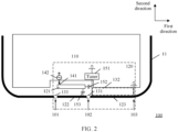
- FIG. 2 is a schematic diagram of a structure of an electronic device 100 according to an embodiment of this application.
- the electronic device 100 may include the side frame 11, an antenna structure 120, and a ground 110.
- a first position 101, a second position 102, and a third position 103 are sequentially disposed on a part of the side frame 11.
- a side frame 11 between the first position 101 and the second position 102 is configured as a first radiator 122 of the antenna structure 120
- a side frame 11 between the second position 102 and the third position 103 is configured as a second radiator 123 of the antenna structure 120.
- the antenna structure 120 may include a third radiator 121 disposed in a housing of the electronic device 100.
- a first slot 131 is provided at the second position 102 of the side frame 11.
- a second slot 132 is formed between the second radiator 123 and the ground 110.
- the first radiator 122 extends in a first direction, and is spaced from the third radiator 121 in a second direction.
- the second direction is perpendicular to the first direction, and projections of the third radiator 121 and the first radiator 122 in the second direction at least partially overlap.
- the third radiator 121 is provided with a first feed point 141, and the first feed point 141 is electrically connected to or in a coupling connection to a feed unit 142, and is configured for feeding the antenna structure 120.
- “Extending in a first direction” in this application should be understood as that the radiator is in a straight strip shape and the straight strip shape extends in the first direction. Alternatively, the radiator is in a bent shape and the bent shape at least partially or integrally extends in the first direction.
- “being spaced in a second direction” should be understood as the radiators are integrally not in contact with each other in the second direction, and specifically, are evenly spaced from each other or are unevenly spaced from each other.
- first position should include a point of the side frame and/or a segment of the side frame.
- a first slot 131 is provided at the second position 102 on the side frame 11 may be understood as that the second position 102 includes the first slot 131 on the side frame, or the second position 102 is a position at which the first slot 131 is provided.
- the second radiator 123 is electrically connected to the ground 110 at the third position 103 may be understood as that the third position 103 is a point on the side frame or a segment on the side frame, and the second radiator 123 includes the third position 103 and is grounded at the third position.
- the second radiator 123 extends inwards from the third position to electrically connect to the ground 110, or the second radiator 123 is specifically connected to a spring contact or a fastening structure at the third position, and the spring contact or the fastening structure is electrically connected to the ground 110.
- the third radiator 121 extends in the first direction, or some edges of the third radiator 121 extend in the first direction. For example, an edge that is on the third radiator 121 and that is close to the first radiator 122 extends in the first direction.
- the third radiator 121 is configured as a feed stub.
- the first feed point 141 may also be disposed on the first radiator 122, and the first radiator 122 is configured as the feed stub for feeding the antenna structure 120. Same technical effect may also be achieved. This is not limited in this application.
- the ground 110 may be understood as any one of the foregoing grounds, or a metal layer electrically connected to any one of the foregoing grounds.
- the first feed point 141 may be disposed at an end that is of the third radiator 121 and that is away from the second radiator 123.
- An end /a first end/a second end (for example, an end of the third radiator 121) of the radiator” mentioned in this application cannot be understood as a point in a narrow sense, and may be considered as a radiator area that includes an endpoint and that is on the third radiator 121.
- a length of the third radiator 121 is L
- it may be considered that the end of the third radiator 121 is an area within 1/4L away from the endpoint.
- the "an end/ a first end/ a second end of the radiator” may be an area within 5 mm away from an end point of the radiator, or an area within 2 mm away from an end point of the radiator.
- the first feed point 141 is disposed at a first end of the first radiator 122, and the first end of the first radiator 122 is an end close to the first position 101.
- the third radiator 121 is configured as a feed stub for feeding the second radiator 123 in an electrical connection or coupling manner, so that the second radiator 123 generates radiation.
- the first radiator 122 and the third radiator 121 are spaced and coupled, and the first radiator 122 and the ground 110 are spaced and coupled.
- a current of the third radiator 121 and a current of the second radiator 123 are basically in a same direction, and a current of the ground 110 and the current of the second radiator 123 are basically reverse. Therefore, the third radiator 121 and the ground 110 respectively generate reverse currents on the first radiator 122, and the reverse currents at least may partially counteract each other.
- the third radiator When the third radiator is configured as the feed stub, the third radiator generates an induced current on the side frame of the electronic device, and the induced current is basically reverse to an induced current generated by the ground on the side frame, so that impact of the current on the ground 110 on the side frame 11 can be reduced. In this way, an SAR is reduced.
- That currents are basically in a same direction may be understood as that main directions (for example, directions of more than 70% of the currents) of the currents are the same.
- That currents are basically reverse may be understood as that main directions (for example, directions of more than 70% of the currents) of the currents are reverse.
- main directions of the currents are in a same direction and are reverse does not mean that the main directions of the currents are in the same direction and are reverse in a spatial sense.
- the shape of the radiator may not be a regular rectangle, and may be a fold line.
- the direction of the current may be understood as a vector direction of the radiator. When a bent portion does not have a current reverse point (zero point), bending of the radiator does not change the direction of the current.
- the antenna structure 120 may have a plurality of operating modes, and the foregoing current distribution analysis may be applied to only one or more of the operating modes, and is not required to be applied to each operating mode. This is not limited in this application.
- an electrical length of the third radiator 121 may be less than a quarter of a first wavelength, and the first wavelength is a wavelength corresponding to an operating frequency band of the antenna structure 120.
- the wavelength corresponding to the operating frequency band of the antenna structure 120 may be considered as a wavelength corresponding to a center frequency of a frequency band supported by the antenna structure 120, or may be considered as a wavelength corresponding to a resonance point generated in the operating frequency band of the antenna structure 120.
- the electrical length may be a ratio of a physical length (namely, a mechanical length or a geometric length) to a wavelength of a transmitted electromagnetic wave.
- resonance generated by the third radiator 121 is located in the operating frequency band of the antenna structure 120, or resonance generated by the third radiator 121 is adjusted to the operating frequency band of the antenna structure 120 in some manners (for example, by adding a matching circuit).
- the first radiator 123 is configured as a main radiator
- the third radiator 121 is configured as a feed stub, so that radiation of the antenna structure 120 in the first operating frequency band is weak. Therefore, an energy distribution ratio of the third radiator 121 and the first radiator 123 is extremely unbalanced.
- the third radiator 121 does not generate resonance in the first operating frequency band of the antenna structure 120, a resonance frequency of the third radiator 121 is higher than a highest frequency in a first operating frequency band of the antenna structure 120, and the second radiator 123 is excited to generate radiation.
- the second radiator 123 may be more fully excited, to ensure a radiation characteristic of the antenna structure 120.
- different operating modes of the antenna structure 120 may be excited by using the third radiator 121, to extend bandwidth of the antenna structure 120.
- the resonance frequency generated by the third radiator 121 may be configured to support the antenna structure 120 in operating in a second operating frequency band, where the second operating frequency band is higher than the first operating frequency band.
- FIG. 3 shows a first operating mode of the antenna structure 120.
- a current of the third radiator 121 and a current of the second radiator 123 are basically in a same direction on two sides of a virtual line.
- the virtual line may be any line between the third radiator 121 and the second radiator 123, and is perpendicular to the first direction.
- (b) in FIG. 3 shows a second operating mode of the antenna structure 120.
- a current of the third radiator 121 and a current of the second radiator 123 are basically reverse on two sides of a virtual line.
- the second radiator 123 is electrically connected to the ground 110 at an end of the first slot 131, and the second radiator 123 is electrically connected to the ground 110 at the third position 103.
- the second radiator 123 is electrically connected to the ground 110 at an end of the first slot 131.
- a third slot 133 is provided at the first position 101 of the side frame 11. Further, the first slot 131 and the third slot 133 may be filled with a medium, to improve physical strength of the side frame 11.
- the second slot 132 may be filled with a plastic particle, for example, a flame-retardant material (FR-4) or another material.
- the antenna structure 120 may further include a tuner (tuner) 151.
- One end of the tuner 151 is electrically connected to the second radiator 123 at an end of the first slot 131, and the other end of the tuner 151 is electrically connected to the ground 110.
- the second radiator 123 generates resonance in an operating frequency band by using the tuner.
- the tuner 151 may be configured to adjust single resonance generated by the antenna structure 120.
- the second radiator 123 switches electrical connection relationships with different electronic elements by using the tuner, to change a resonant frequency band of the antenna structure 120, so that the antenna structure 120 operates in different frequency band ranges.
- the third radiator 121 in the antenna structure 120 performs feeding on the second radiator 123 in a manner of electrically connecting to or coupling to the second radiator 123.
- the third radiator 121 and the second radiator 123 are spaced in a direction, and projections of the third radiator 121 and the second radiator 123 in the direction at least partially overlap, to provide the foregoing coupling manner.
- a direction in which the third radiator 121 and the second radiator 123 are spaced may be the first direction, the second direction, or any other direction, and is set based on a spatial layout in a housing of the electronic device. This is not limited in this application.
- the antenna structure 120 may further include a capacitor 152.
- the capacitor 152 may be connected in series between the third radiator 121 and the second radiator 123. One end of the capacitor 152 is electrically connected to the third radiator 121, and the other end of the capacitor 152 is electrically connected to the second radiator 123. For example, one end of the capacitor 152 may be electrically connected to the second radiator 123 at an end of the first slot 131, and the other end of the capacitor 152 may be electrically connected to an end of the third radiator 121.
- energy transmitted from the third radiator 121 to the second radiator 123 may be controlled, to control a radiation characteristic of the antenna structure 120.
- a capacitance value of the capacitor 152 is less than or equal to 1 pF. In this embodiment of this application, only an example in which a capacitance value of the capacitor 152 is 0.2 pF is used for description. During actual application, the capacitance value may be adjusted based on a production or design requirement. This is not limited in this application.
- the antenna structure may further include a capacitor 153.
- the capacitor 153 may be connected in series between the third radiator 121 and the first radiator 122. A first end of the capacitor 153 is electrically connected to the third radiator 121, and a second end of the capacitor 153 is electrically connected to the first radiator 122. In an embodiment, a second end of the capacitor 153 may be electrically connected to the first radiator 122 at an end of the first slot 131. In an embodiment, a first end of the capacitor 153 may be electrically connected to an end that is of the third radiator 121 and that is close to the second position 102. In an embodiment, by adjusting a capacitance value of the capacitor 153, energy transmitted from the third radiator 121 to the first radiator 122 may be controlled, to control a radiation characteristic of the antenna structure 120.
- the third radiator 121 may have a part that bends towards the second radiator 123, and/or the second radiator 123 may have a part that bends towards the third radiator 121, to provide the foregoing electrical connection or coupling manner on the bent part.
- FIG. 4 and FIG. 9 are diagrams of simulation results of an antenna structure shown in FIG. 2 .
- FIG. 4 is an S-parameter simulation diagram of an antenna structure shown in FIG. 2 .
- FIG. 5 is a Smith chart of an antenna structure shown in FIG. 2 .
- FIG. 6 is a schematic diagram of current distribution of an antenna structure shown in FIG. 2 at 1.8 GHz.
- FIG. 7 is a schematic diagram of current distribution of an antenna structure shown in FIG. 2 at 2.3 GHz.
- FIG. 8 is a pattern of an antenna structure shown in FIG. 2 at 1.8 GHz.
- FIG. 9 is a pattern of an antenna structure shown in FIG. 2 at 2.3 GHz.
- a resonant frequency band of the antenna structure may include 1.86 GHz to 2.32 GHz, and may include a transmit frequency band (1920 MHz to 1980 MHz) and a receive frequency band (2110 MHz to 2170 MHz) of a B1 frequency band in LTE, so that an electronic device can operate normally in the B1 frequency band.
- frequencies 1.78 GHz and 2.44 GHz are respectively located on two sides of a zero axis. It is generally considered that when a curve passes through the zero axis once, the antenna structure has one operating mode. Therefore, the antenna structure has two operating modes, which correspond to the operating modes of the antenna structure shown in FIG. 3 .
- FIG. 6 is a schematic diagram of current distribution of an antenna structure at 1.8 GHz.
- a current of the third radiator 121 and a current of the second radiator 123 are basically in a same direction on two sides of a virtual line, and correspond to the first operating mode of the antenna structure shown in (a) in FIG. 3 . Therefore, resonance generated in the first operating mode of the antenna structure is mainly located in a low frequency band in the operating frequency band of the antenna structure, and may include the transmit frequency band (1920 MHz to 1980 MHz) of the B1 frequency band.
- FIG. 7 is a schematic diagram of current distribution of an antenna structure at 2.3 GHz.
- a current of the third radiator 121 and a current of the second radiator 123 are basically reverse in direction on two sides of a virtual line, and correspond to the second operating mode of the antenna structure shown in (b) in FIG. 3 . Therefore, resonance generated in the first operating mode of the antenna structure is mainly located in a high frequency band in the operating frequency band of the antenna structure, and may include the receive frequency band (2110 MHz to 2170 MHz) of the B1 frequency band.
- the maximum radiation directions of the antenna structure at 1.8 GHz and 2.3 GHz are basically perpendicular. Therefore, directions covered by the first operating mode and the second operating mode of the antenna structure are different.
- the maximum radiation direction of the antenna structure may be adjusted based on different handheld manners of the user, to effectively improve user experience and avoid signal fading caused by a handheld posture of the user.
- FIG. 10 and FIG. 11 are schematic diagrams of an electronic device according to an embodiment of this application.
- FIG. 10 is a schematic diagram of a cross section of an electronic device in a second direction.
- FIG. 11 is a schematic diagram of current distribution according to an embodiment of this application.
- the third radiator 121 is located between the ground 110 and the rear cover 21 of the electronic device in a third direction, where the third direction is a thickness direction of the electronic device.
- a spacing between the third radiator 121 and the rear cover 21 is less than a spacing between the ground 110 and the rear cover 21.
- the third radiator 121 is located between the ground 110 and the cover glass 13 of the electronic device in the third direction.
- a spacing between the third radiator 121 and the cover glass 13 is less than a spacing between the ground 110 and the cover glass 13. It should be understood that the third radiator 121 may be partially or completely staggered with the ground 110 in the third direction.
- the third radiator 121 may be disposed on a support between the ground 110 and the rear cover 21/cover glass 13 of the electronic device.
- the third radiator 121 is formed by embedding a steel sheet in the support, or the third radiator 121 is formed on the support by using a laser-direct-structuring (laser-direct-structuring, LDS) technology.
- LDS laser-direct-structuring
- the third radiator 121 may alternatively be implemented in another manner, for example, implemented in a form of a floating metal (floating metal, FLM) or a flexible circuit board (flexible printed circuit, FPC). This is not limited in this application.
- the third radiator 121 is a metal sheet, for example, a steel sheet, and the metal sheet is disposed in an extension direction of the ground 110.
- a thickness of the metal sheet is less than a thickness of the side frame 11, for example, less than a thickness of a narrowest part of the side frame 11.
- the third radiator 121 may be in a rectangular shape, a broken line shape, a U shape, or an irregular shape. This is not limited in this application. In an embodiment, a shape, a size, a thickness, and the like of the third radiator 121 may be adjusted based on relative positions between the ground 110, the first radiator 122, the second radiator 123, and the third radiator 121, to effectively use internal space of the electronic device.
- a parameter like a shape, a size, a thickness, or an electrical length of the third radiator 121 may be further adjusted based on an actual production or design requirement, so that an amplitude of a second induced current generated by the third radiator 121 on the first radiator 122 is approximately the same as an amplitude of the first induced current. In this way, an SAR of the antenna structure is effectively reduced.
- the SAR is used as a transmit index of the antenna.
- an operating mode corresponding to the transmit frequency band (1920 MHz to 1980 MHz) of the antenna structure is the first operating mode, as shown in (a) in FIG. 3 .
- a first slot and a third slot are provided at a first position and a second position of the side frame 11.
- the first radiator 122 is a floating stub, and two ends of the first radiator 122 are not electrically connected to the ground 110.
- a current of the first radiator 122 mainly includes two parts: One part is a first induced current caused on the first radiator 122 due to a current generated by a radiation stub (the second radiator 123) of the antenna structure on the ground 110, and the first induced current is basically in a same direction as a current on the second radiator 123.
- the other part is a second induced current generated on the first radiator 122 by a feed stub (the third radiator 121) of the antenna structure, the second induced current is basically reverse to a current on the third radiator 121. That is, both the first introduced current and the second introduced current exist on the first radiator 122, and directions of the first introduced current and the second introduced current are reverse.
- a presented result is that at least some currents counteract each other, and a current zero point appears.
- a part of the side frame of the electronic device is configured as a radiator.
- a relative position of the third radiator 121 may be adjusted by adjusting a relative position of the third radiator 121 and a capacitance value of a capacitor between the third radiator 121 and the second radiator 123, that is, relative positions of the ground 110, the first radiator 122, and the second radiator 123, and the third radiator 121 are adjusted by adjusting the relative position of the third radiator. Because an amplitude of the second induced current generated by the third radiator 121 on the first radiator 122 is the same as an amplitude of the first induced current, an SAR of the antenna structure is effectively reduced.
- the first radiator 122 is configured to at least partially cancel the first induced current and the second induced current in a resonant frequency band generated by the second radiator 123, and the first radiator 122 does not generate resonance in the resonant frequency band generated by the second radiator 123.
- a resonant frequency band generated by the first radiator 122 may be outside the resonant frequency band generated by the second radiator 123.
- a length of the first radiator 122 may be different from a length of the second radiator 123, the length of the first radiator 122 may be greater than or less than the length of the second radiator 123, and the resonant frequency band generated by the first radiator 122 may be higher than or less than the resonant frequency band generated by the second radiator 123.
- the length may be understood as an electrical length or a physical length.
- the resonant frequency band generated by the first radiator 122 may be configured to extend a communication frequency band of the antenna structure, so that the antenna structure operates in more communication frequency bands, to improve user experience.
- a following position at which the third radiator 121 is disposed affects an amplitude of the second induced current generated by the third radiator 121 on the first radiator 122: 1.
- an angle ⁇ between the third radiator 121 and the first radiator 122 In a plane formed by the first direction and the second direction, an angle ⁇ between the third radiator 121 and the first radiator 122, namely, an area of the third radiator 121 facing the first radiator 122. 3.
- a medium between the third radiator 121 and the first radiator 122 This is not limited in this application, and the foregoing is merely used as an example.
- FIG. 12 is a schematic diagram of magnetic field distribution of an antenna structure shown in FIG. 2 .
- magnetic fields generated by using a first induced current and a second induced current in opposite phases counteract each other.
- a magnetic field near the first radiator has a zero point (or a close to zero point), and a magnetic field of the antenna structure has no strong point, so that an SAR of the antenna structure can be effectively reduced.
- FIG. 13 is a schematic diagram of another antenna structure according to an embodiment of this application.
- a difference between the antenna structure and the antenna structure shown in FIG. 2 lies only in that the antenna structure does not include a third radiator, and the first radiator is configured as a feed stub for feeding the antenna structure.
- the other parts of the antenna structure are the same as those of the antenna structure shown in FIG. 2 .
- the antenna structure shown in FIG. 13 is used as an antenna structure for comparison in this application.
- Table 1 shows measured results of the antenna structure shown in FIG. 2 and the antenna structure shown in FIG. 13 .
- Table 1 Antenna structure shown in FIG. 2 Antenna structure shown in FIG. 13 Free space (free space, FS) efficiency -1.23 dB -2.1 dB SAR 2 W/Kg 2.65 W/Kg Normalized SAR (-4 dB) 1.06 W/Kg 1.75 W/Kg
- an SAR value of the antenna structure (the antenna structure shown in FIG. 2 ) provided in this embodiment of this application is greatly improved compared with that of the compared antenna structure (the antenna structure shown in FIG. 13 ).
- FIG. 14 is a schematic diagram of a structure of an electronic device 200 according to an embodiment of this application.
- the electronic device 200 may include the side frame 11, a ground 210, and an antenna structure 220.
- a first position 201, a second position 202, and a third position 203 are sequentially disposed on a part of the side frame 11.
- a side frame 11 between the first position 201 and the second position 202 is configured as a first radiator 222 of the antenna structure 220
- a side frame 11 between the second position 202 and the third position 203 is configured as a second radiator 223 of the antenna structure 220.
- a first slot 231 is provided at the second position 202 of the side frame 11.
- a second slot 232 is formed between the second radiator 223 and the ground 210.
- the first radiator 222 is not provided with a slot at the first position 201, and the first radiator 222 is electrically connected to the ground 210 at the first position 201.
- the second radiator 223 is not provided with a slot at the third position 203, and the second radiator 222 is electrically connected to the ground 210 at the third position 203.
- the antenna structure 220 may include a third radiator 221 disposed in a housing of the electronic device 200.
- the first radiator 222 extends in a first direction, and is spaced from the third radiator 221 in a second direction.
- the second direction is perpendicular to the first direction, and projections of the third radiator 221 and the first radiator 222 in the second direction at least partially overlap.
- the third radiator 221 is provided with a first feed point 241, and the first feed point 241 is electrically connected to a feed unit 242, and is configured for feeding the antenna structure 220.
- the third radiator 221 extends in the first direction, or some edges of the third radiator 221 extend in the first direction. For example, an edge that is on the third radiator 221 and that is close to the first radiator 222 extends in the first direction.
- the third radiator 221 in the antenna structure 120 performs feeding on the second radiator 223 in a manner of electrically connecting to or coupling to the second radiator 223.
- the third radiator 221 and the second radiator 223 are spaced in a direction, and projections of the third radiator 221 and the second radiator 223 in the direction at least partially overlap, to provide the foregoing coupling manner.
- a direction in which the third radiator 221 and the second radiator 223 are spaced may be the first direction, the second direction, or any other direction, and is set based on a spatial layout in a housing of the electronic device. This is not limited in this application.
- the antenna structure 220 may further include a first capacitor 251.
- the first capacitor 251 may be connected in series between the third radiator 221 and the second radiator 223.
- a first end of the first capacitor 251 is electrically connected to the third radiator 221, and a second end of the first capacitor 251 is electrically connected to the second radiator 223.
- a first end of the first capacitor 251 may be electrically connected to an end that is of the third radiator 221 and that is close to the second position 202.
- a second end of the first capacitor 251 may be electrically connected to the second radiator 223 at an end of the first slot 231.
- energy transmitted from the third radiator 221 to the second radiator 223 may be controlled, to control a radiation characteristic of the antenna structure 220.
- a capacitance value of the first capacitor 251 is less than or equal to 1 pF. In this embodiment of this application, only an example in which a capacitance value of the first capacitor 251 is 0.2 pF is used for description. During actual application, the capacitance value may be adjusted based on a production or design requirement. This is not limited in this application.
- the third radiator 221 may have a part that bends towards the second radiator 223, and/or the second radiator 223 may have a part that bends towards the third radiator 221, to provide the foregoing electrical connection or coupling manner on the bent part.
- the third radiator 221 is configured as a feed stub for feeding the second radiator 223 in an electrical connection or coupling manner, so that the second radiator 223 generates radiation.
- the first radiator 222 is electrically connected to or coupled to the third radiator 221, and the first radiator 222 is electrically connected to the ground 210 at the first position 201.
- a current of the third radiator 221 and a current of the second radiator 223 are basically in a same direction, and a current of the ground 110 and the current of the second radiator 123 are basically reverse. Therefore, the third radiator 121 and the ground 110 respectively generate reverse included currents on the first radiator 122, and the reverse induced currents at least may partially counteract each other.
- the third radiator When the third radiator is configured as the feed stub, the third radiator generates a current on the side frame of the electronic device, and the current is basically reverse to a current generated by the ground on the side frame, so that impact of the current on the ground 110 on the side frame 11 can be reduced. In this way, an SAR is reduced.
- the third radiator 221 and the first radiator 222 are spaced by a specific distance, to provide the foregoing coupling manner.
- the antenna structure 220 may further include a second capacitor 252.
- the second capacitor 252 may be connected in series between the third radiator 221 and the first radiator 222.
- a first end of the second capacitor 252 is electrically connected to the third radiator 221, and a second end of the second capacitor 252 is electrically connected to the first radiator 222.
- a second end of the second capacitor 252 may be electrically connected to the first radiator 222 at an end of the first slot 231.
- a first end of the second capacitor 252 may be electrically connected to an end that is of the third radiator 221 and that is close to the second position 202.
- by adjusting a capacitance value of the second capacitor 252 energy transmitted from the third radiator 221 to the first radiator 222 may be controlled, to control a radiation characteristic of the antenna structure 220.
- a capacitance value of the second capacitor 252 is less than or equal to 1 pF. In this embodiment of this application, only an example in which a capacitance value of the second capacitor 252 is 0.2 pF is used for description. During actual application, the capacitance value may be adjusted based on a production or design requirement. This is not limited in this application.
- the third radiator 221 may have a part that bends towards the first radiator 222, and/or the first radiator 222 may have a part that bends towards the third radiator 221, to provide the foregoing electrical connection or coupling manner on the bent part.
- the antenna structure 220 may further include a tuner 253.
- One end of the tuner 253 is electrically connected to the second radiator 223 at an end of the first slot 231, and the other end of the tuner 253 is electrically connected to the ground 210.
- the tuner 253 may be configured to switch between different electronic elements electrically connected to the second radiator 223, to change resonance of the antenna structure 120, so that the antenna structure 120 operates in different frequency bands.
- the tuner 253 may alternatively be disposed at the third position 203 and connected between the ground 310 and the second radiator 223. This is not limited in this application.
- an electrical length of the third radiator 221 may be less than a quarter of a first wavelength, and the first wavelength is a wavelength corresponding to an operating frequency band of the antenna structure 220.
- Resonance generated by the third radiator 221 is located in the operating frequency band of the antenna structure 220, or resonance generated by the third radiator 221 is adjusted to the operating frequency band of the antenna structure 220 in some manners (for example, by adding a matching circuit). This is similar to that in the foregoing embodiment, and details are not described herein again.
- a relative position (for example, between the ground 110 and the rear cover 21/cover glass 13 of the electronic device) of the third radiator 221 in the electronic device, an implementation form (for example, a steel sheet embedded in the support, an LDS, a floating metal, or a flexible circuit board), a shape of the third radiator 221, or the like are similar to that in the foregoing embodiment. Details are not described herein again.
- FIG. 15 is an S-parameter simulation diagram of an antenna structure shown in FIG. 14 .
- a resonant frequency band of the antenna structure may include a transmit frequency band (1920 MHz to 1980 MHz) and a receive frequency band (2110 MHz to 2170 MHz) of a B1 frequency band in LTE, so that an electronic device can operate normally in the B1 frequency band.
- FIG. 16 is a schematic diagram of current distribution according to an embodiment of this application.
- a current of the first radiator 222 mainly includes two parts: One part is a first induced current caused on the first radiator 222 due to a current generated by a radiation stub (the second radiator 223) of the antenna structure on the ground 210, and the first induced current is basically in a same direction as a current on the second radiator 223.
- the other part is a second induced current generated on the first radiator 222 by a feed stub (the third radiator 221) of the antenna structure, the second induced current is basically reverse to a current on the third radiator 221.
- both the first introduced current and the second introduced current exist on the first radiator 222, and directions of the first introduced current and the second introduced current are reverse.
- a presented result is that at least some currents counteract each other, and a current zero point appears.
- magnetic fields generated by the first induced current and the second induced current in opposite phases counteract each other, and a zero point (or a close to zero point) of the magnetic field appears. In this way, an SAR of the antenna structure is reduced.
- the first radiator 222 is configured to at least partially cancel the first induced current and the second induced current in a resonant frequency band generated by the second radiator 223. Therefore, the first radiator 222 does not generate resonance in the resonant frequency band generated by the second radiator 223, and a resonant frequency band generated by the first radiator 222 should be outside the resonant frequency band generated by the second radiator 223.
- a resonant frequency band generated by the first radiator 222 should be outside the resonant frequency band generated by the second radiator 223.
- an SAR value is high.
- a length of the first radiator 222 may be greater than a length of the second radiator 223, so that a resonant frequency band generated by the first radiator 222 may be lower than a resonant frequency band generated by the second radiator 223.
- the length may be understood as an electrical length or a physical length.
- the resonant frequency band generated by the first radiator 222 may be configured to extend a low-frequency communication frequency band of the antenna structure, so that the antenna structure operates in more communication frequency bands, to improve user experience.
- FIG. 17 is a schematic diagram of another antenna structure according to an embodiment of this application.
- a difference between the antenna structure and the antenna structure shown in FIG. 14 lies only in that the antenna structure does not include a third radiator, and the first radiator is configured as a feed stub for feeding the antenna structure.
- the other parts of the antenna structure are the same as those of the antenna structure shown in FIG. 14 .
- the antenna structure shown in FIG. 17 is configured as an antenna structure for comparison in this application.
- FIG. 18 and FIG. 19 are respectively schematic diagrams of magnetic field distribution of the antenna structures shown in FIG. 14 and FIG. 17 .
- the antenna structure shown in FIG. 14 uses the first induced current and the second induced current in opposite phases (with a phase difference of approximately 180°), so that generated magnetic fields counteract each other.
- the magnetic fields generated by the antenna structure are distributed evenly, and there is no strong point in several areas of the magnetic fields of the antenna structure, so that an SAR of the antenna structure can be effectively reduced.
- Table 2 and Table 3 show measured results of the antenna structure shown in FIG. 14 and the antenna structure shown in FIG. 17 .
- Table 2 (Antenna structure shown in FIG. 14) Test frequency band FS efficiency SAR Normalized SAR (-4 dB) B3 -4 dB 1.1 W/Kg 1.1 W/Kg B1 -3.2 dB 1.31 W/Kg 1.08 W/Kg B7 -3.4 dB 1.02 W/Kg 0.9 W/Kg Table 3 (Antenna structure shown in FIG.
- the disclosed system, apparatus, and method may be implemented in another manner.
- the described apparatus embodiment is merely an example.
- division into the units is merely logical function division and may be other division during actual implementation.
- a plurality of units or components may be combined or integrated into another system, or some features may be ignored or not performed.
- the displayed or discussed mutual couplings or direct couplings or communication connections may be implemented through some interfaces.
- the indirect couplings or communication connections between the apparatuses or units may be implemented in electronic or other forms.
Landscapes
- Engineering & Computer Science (AREA)
- Computer Hardware Design (AREA)
- General Engineering & Computer Science (AREA)
- Computer Networks & Wireless Communication (AREA)
- Support Of Aerials (AREA)
Applications Claiming Priority (2)
| Application Number | Priority Date | Filing Date | Title |
|---|---|---|---|
| CN202111111392.5A CN115842238B (zh) | 2021-09-18 | 2021-09-18 | 一种电子设备 |
| PCT/CN2022/118906 WO2023040928A1 (fr) | 2021-09-18 | 2022-09-15 | Dispositif électronique |
Publications (2)
| Publication Number | Publication Date |
|---|---|
| EP4391226A1 true EP4391226A1 (fr) | 2024-06-26 |
| EP4391226A4 EP4391226A4 (fr) | 2024-12-25 |
Family
ID=85574447
Family Applications (1)
| Application Number | Title | Priority Date | Filing Date |
|---|---|---|---|
| EP22869297.6A Pending EP4391226A4 (fr) | 2021-09-18 | 2022-09-15 | Dispositif électronique |
Country Status (4)
| Country | Link |
|---|---|
| US (1) | US20250141089A1 (fr) |
| EP (1) | EP4391226A4 (fr) |
| CN (1) | CN115842238B (fr) |
| WO (1) | WO2023040928A1 (fr) |
Families Citing this family (9)
| Publication number | Priority date | Publication date | Assignee | Title |
|---|---|---|---|---|
| CN118712716B (zh) * | 2023-03-27 | 2026-01-09 | 华为技术有限公司 | 一种电子设备 |
| CN116598762B (zh) * | 2023-04-28 | 2026-04-07 | 维沃移动通信有限公司 | 电子设备 |
| CN116799488A (zh) * | 2023-06-28 | 2023-09-22 | 维沃移动通信有限公司 | 天线模组和电子设备 |
| CN119518266B (zh) * | 2023-08-23 | 2025-11-11 | Oppo广东移动通信有限公司 | 电子设备 |
| CN120165221A (zh) * | 2023-12-14 | 2025-06-17 | 华为技术有限公司 | 一种可穿戴设备 |
| CN121399793A (zh) * | 2023-12-26 | 2026-01-23 | 荣耀终端股份有限公司 | 一种电子设备 |
| CN120237405A (zh) * | 2023-12-29 | 2025-07-01 | 华为技术有限公司 | 一种电子设备 |
| CN120566052A (zh) * | 2024-02-29 | 2025-08-29 | 华为技术有限公司 | 一种电子设备 |
| CN121460949A (zh) * | 2024-07-31 | 2026-02-03 | 华为技术有限公司 | 电子设备 |
Family Cites Families (18)
| Publication number | Priority date | Publication date | Assignee | Title |
|---|---|---|---|---|
| JP2002185238A (ja) * | 2000-12-11 | 2002-06-28 | Sony Corp | デュアルバンド対応内蔵アンテナ装置およびこれを備えた携帯無線端末 |
| CN106450658A (zh) * | 2015-08-07 | 2017-02-22 | 微软技术许可有限责任公司 | 用于电子设备的天线装置 |
| KR102534531B1 (ko) * | 2016-07-29 | 2023-05-19 | 삼성전자주식회사 | 복수의 안테나를 포함하는 전자 장치 |
| US10944151B2 (en) * | 2017-02-24 | 2021-03-09 | Chiun Mai Communication Systems, Inc. | Antenna structure and wireless communication device using same |
| TWI643397B (zh) * | 2017-08-22 | 2018-12-01 | 廣達電腦股份有限公司 | 行動裝置 |
| EP3451636B1 (fr) * | 2017-08-30 | 2025-09-17 | LG Electronics Inc. | Terminal mobile |
| CN109830815B (zh) * | 2018-12-24 | 2021-04-02 | 瑞声科技(南京)有限公司 | 天线系统及应用该天线系统的移动终端 |
| CN111864349B (zh) * | 2019-04-26 | 2021-12-28 | 北京小米移动软件有限公司 | 移动终端及移动终端的天线辐射方法 |
| CN112531331B (zh) * | 2019-09-18 | 2022-04-12 | 华为技术有限公司 | 一种天线及终端设备 |
| CN112689033B (zh) * | 2019-10-18 | 2022-07-22 | 荣耀终端有限公司 | 终端设备 |
| KR20210054262A (ko) * | 2019-11-05 | 2021-05-13 | 삼성전자주식회사 | 안테나 구조체 및 이를 포함하는 전자 장치 |
| CN112886232B (zh) * | 2019-11-30 | 2022-10-11 | 华为技术有限公司 | 电子设备 |
| CN113078444B (zh) * | 2020-01-06 | 2024-06-11 | 深圳富泰宏精密工业有限公司 | 天线结构及具有该天线结构的无线通信装置 |
| CN116487893A (zh) * | 2020-01-17 | 2023-07-25 | 荣耀终端有限公司 | 天线结构及具有该天线结构的电子设备 |
| CN111987454A (zh) * | 2020-08-06 | 2020-11-24 | 惠州Tcl移动通信有限公司 | 一种mimo多天线结构及移动终端 |
| CN113013594B (zh) * | 2021-02-26 | 2023-07-28 | Oppo广东移动通信有限公司 | 天线组件和电子设备 |
| CN113922048B (zh) * | 2021-05-28 | 2022-09-30 | 荣耀终端有限公司 | 一种终端天线及终端电子设备 |
| KR20230027914A (ko) * | 2021-08-20 | 2023-02-28 | 삼성전자주식회사 | 안테나를 포함하는 전자 장치 |
-
2021
- 2021-09-18 CN CN202111111392.5A patent/CN115842238B/zh active Active
-
2022
- 2022-09-15 US US18/692,697 patent/US20250141089A1/en active Pending
- 2022-09-15 WO PCT/CN2022/118906 patent/WO2023040928A1/fr not_active Ceased
- 2022-09-15 EP EP22869297.6A patent/EP4391226A4/fr active Pending
Also Published As
| Publication number | Publication date |
|---|---|
| WO2023040928A1 (fr) | 2023-03-23 |
| CN115842238B (zh) | 2025-11-14 |
| CN115842238A (zh) | 2023-03-24 |
| EP4391226A4 (fr) | 2024-12-25 |
| US20250141089A1 (en) | 2025-05-01 |
Similar Documents
| Publication | Publication Date | Title |
|---|---|---|
| EP4391226A1 (fr) | Dispositif électronique | |
| EP4421988A1 (fr) | Structure d'antenne et dispositif électronique | |
| EP4557509A1 (fr) | Dispositif électronique | |
| JP5599472B2 (ja) | 電気的接地への周波数依存性接続を有するアンテナデバイス | |
| EP4510385A1 (fr) | Unité d'antenne et dispositif électronique | |
| EP4391230A1 (fr) | Dispositif électronique | |
| US20250004424A1 (en) | Wearable device | |
| EP4648226A1 (fr) | Structure d'antenne et dispositif électronique | |
| EP4528923A1 (fr) | Système d'antenne et dispositif électronique | |
| EP4362227A1 (fr) | Structure d'antenne et dispositif électronique | |
| US12562477B2 (en) | Antenna and electronic device | |
| EP4621991A1 (fr) | Dispositif électronique | |
| EP4531205A1 (fr) | Dispositif électronique | |
| CN117996436B (zh) | 一种电子设备 | |
| EP4528929A1 (fr) | Dispositif électronique | |
| CN118712716B (zh) | 一种电子设备 | |
| Sasaki et al. | 21 MHz/2.4 GHz Dual-use Wearable Antenna for IEEE 802.15. 6 Wireless Body Area Network | |
| CN205646153U (zh) | 具有金属外壳的电子设备中的天线及其电子设备 | |
| US20190356041A1 (en) | Terminal | |
| EP4557519A1 (fr) | Structure d'antenne et dispositif électronique | |
| CN114156633B (zh) | 低sar天线装置及电子设备 | |
| EP4471985A1 (fr) | Dispositif électronique | |
| CN222562967U (zh) | 一种天线结构及电子设备 | |
| EP4462596A1 (fr) | Structure d'antenne et dispositif électronique | |
| CN121149654A (zh) | 一种通信终端 |
Legal Events
| Date | Code | Title | Description |
|---|---|---|---|
| STAA | Information on the status of an ep patent application or granted ep patent |
Free format text: STATUS: THE INTERNATIONAL PUBLICATION HAS BEEN MADE |
|
| PUAI | Public reference made under article 153(3) epc to a published international application that has entered the european phase |
Free format text: ORIGINAL CODE: 0009012 |
|
| STAA | Information on the status of an ep patent application or granted ep patent |
Free format text: STATUS: REQUEST FOR EXAMINATION WAS MADE |
|
| 17P | Request for examination filed |
Effective date: 20240320 |
|
| AK | Designated contracting states |
Kind code of ref document: A1 Designated state(s): AL AT BE BG CH CY CZ DE DK EE ES FI FR GB GR HR HU IE IS IT LI LT LU LV MC MK MT NL NO PL PT RO RS SE SI SK SM TR |
|
| REG | Reference to a national code |
Ref country code: DE Ref legal event code: R079 Free format text: PREVIOUS MAIN CLASS: H01Q0001360000 Ipc: H01Q0001240000 |
|
| A4 | Supplementary search report drawn up and despatched |
Effective date: 20241125 |
|
| DAV | Request for validation of the european patent (deleted) | ||
| DAX | Request for extension of the european patent (deleted) | ||
| RIC1 | Information provided on ipc code assigned before grant |
Ipc: H01Q 5/385 20150101ALI20241119BHEP Ipc: H01Q 5/371 20150101ALI20241119BHEP Ipc: H01Q 5/328 20150101ALI20241119BHEP Ipc: H01Q 9/42 20060101ALI20241119BHEP Ipc: H01Q 1/24 20060101AFI20241119BHEP |