EP4391265A1 - Reduzierung des einschaltstroms zu einer kondensatorbank - Google Patents
Reduzierung des einschaltstroms zu einer kondensatorbank Download PDFInfo
- Publication number
- EP4391265A1 EP4391265A1 EP22216194.5A EP22216194A EP4391265A1 EP 4391265 A1 EP4391265 A1 EP 4391265A1 EP 22216194 A EP22216194 A EP 22216194A EP 4391265 A1 EP4391265 A1 EP 4391265A1
- Authority
- EP
- European Patent Office
- Prior art keywords
- phase
- voltage
- switching device
- phases
- waveform
- Prior art date
- Legal status (The legal status is an assumption and is not a legal conclusion. Google has not performed a legal analysis and makes no representation as to the accuracy of the status listed.)
- Pending
Links
Images


Classifications
-
- H—ELECTRICITY
- H02—GENERATION; CONVERSION OR DISTRIBUTION OF ELECTRIC POWER
- H02H—EMERGENCY PROTECTIVE CIRCUIT ARRANGEMENTS
- H02H9/00—Emergency protective circuit arrangements for limiting excess current or voltage without disconnection
- H02H9/02—Emergency protective circuit arrangements for limiting excess current or voltage without disconnection responsive to excess current
-
- H—ELECTRICITY
- H01—ELECTRIC ELEMENTS
- H01H—ELECTRIC SWITCHES; RELAYS; SELECTORS; EMERGENCY PROTECTIVE DEVICES
- H01H9/00—Details of switching devices, not covered by groups H01H1/00 - H01H7/00
- H01H9/54—Circuit arrangements not adapted to a particular application of the switching device and for which no provision exists elsewhere
- H01H9/56—Circuit arrangements not adapted to a particular application of the switching device and for which no provision exists elsewhere for ensuring operation of the switch at a predetermined point in the AC cycle
- H01H9/563—Circuit arrangements not adapted to a particular application of the switching device and for which no provision exists elsewhere for ensuring operation of the switch at a predetermined point in the AC cycle for multipolar switches, e.g. different timing for different phases, selecting phase with first zero-crossing
-
- H—ELECTRICITY
- H02—GENERATION; CONVERSION OR DISTRIBUTION OF ELECTRIC POWER
- H02H—EMERGENCY PROTECTIVE CIRCUIT ARRANGEMENTS
- H02H1/00—Details of emergency protective circuit arrangements
- H02H1/04—Arrangements for preventing response to transient abnormal conditions, e.g. to lightning or to short duration over voltage or oscillations; Damping the influence of DC component by short circuits in AC networks
- H02H1/043—Arrangements for preventing response to transient abnormal conditions, e.g. to lightning or to short duration over voltage or oscillations; Damping the influence of DC component by short circuits in AC networks to inrush currents
-
- H—ELECTRICITY
- H02—GENERATION; CONVERSION OR DISTRIBUTION OF ELECTRIC POWER
- H02H—EMERGENCY PROTECTIVE CIRCUIT ARRANGEMENTS
- H02H7/00—Emergency protective circuit arrangements specially adapted for specific types of electric machines or apparatus or for sectionalised protection of cable or line systems, and effecting automatic switching in the event of an undesired change from normal working conditions
- H02H7/16—Emergency protective circuit arrangements specially adapted for specific types of electric machines or apparatus or for sectionalised protection of cable or line systems, and effecting automatic switching in the event of an undesired change from normal working conditions for capacitors
-
- H—ELECTRICITY
- H02—GENERATION; CONVERSION OR DISTRIBUTION OF ELECTRIC POWER
- H02H—EMERGENCY PROTECTIVE CIRCUIT ARRANGEMENTS
- H02H9/00—Emergency protective circuit arrangements for limiting excess current or voltage without disconnection
- H02H9/001—Emergency protective circuit arrangements for limiting excess current or voltage without disconnection limiting speed of change of electric quantities, e.g. soft switching on or off
Definitions
- the present disclosure relates to reducing inrush current to an ungrounded capacitor bank when re-closing a switching device arranged between an AC voltage source and the capacitor bank in an electrical three-phase system.
- an inrush current will occur with a magnitude that depends on the closing angle at which energization occurs.
- Optimal closing angles can be found, in relation to the system voltages, to minimize the inrush current if the initial state of the capacitor bank is that it is fully discharged, e.g. 5 minutes after the capacitor bank being disconnected. If the bank is ungrounded, any two of the circuit breaker poles are closed first, when the corresponding line-to-line voltage is zero, and the third pole is closed one quarter of a period later.
- the capacitor bank has just recently been disconnected, it will still be fully charged, or partially charged, depending on how long time has elapsed since the disconnecting.
- minimizing the inrush current is not achieved by the same closing sequence as when the capacitor bank is fully discharged.
- the present invention relates to reducing inrush current to an ungrounded capacitor bank also when re-connecting of the capacitor bank is done before it has been fully discharged.
- a method for reducing inrush current to an ungrounded capacitor bank when re-closing a switching device arranged between an AC voltage source and the capacitor bank in an electrical three-phase system comprises opening the switching device by an opening sequence.
- the opening sequence comprises breaking the current of a first phase of the three phases, and after a predetermined opening time period starting at the breaking of the first phase, simultaneously breaking the current of a second phase of the three phases and the current of a third phase of the three phases.
- the method also comprises, following the opening, closing the switching device, by a closing sequence.
- the closing sequence comprises simultaneously making the respective currents of the second and third phases, and after a predetermined closing time period starting at the making of the second and third phases, making the current of the first phase.
- the predetermined opening time period corresponds to a 1/4+m period or a 3/4+m period of a voltage waveform of anyone of the three phases, where m is an integer of at least zero, preferably zero. If the predetermined opening time period corresponds to a 1/4+m period, the predetermined closing time period corresponds to a 3/4+n period of the voltage waveform. If the predetermined opening time period corresponds to a 3/4+m period, the predetermined closing time period corresponds to a 1/4+n period of the voltage waveform, n is an integer of at least zero, preferably zero.
- a computer program product comprising computer-executable components for causing a controller to perform an embodiment of the method of the present disclosure when the computer-executable components are run on processing circuitry comprised in the controller.
- a controller for a switching device comprises processing circuitry, and storage storing instructions executable by said processing circuitry whereby said controller is operative to perform an embodiment of the method of the present disclosure.
- an electrical three-phase system comprising an embodiment of the controller of the present disclosure, the switching device, and the capacitor bank.
- the two phases which were opened last are closed first, before closing the phase which was opened first. It has now been realized that the inrush current may be reduced even when the capacitor bank has not yet fully discharged after the opening of the switching device. According to the invention, this is achieved by using a specific predetermined closing time period between the making of the second and third phases and the making of the first phase. This predetermined closing time period depends on the predetermined opening time period.
- closing sequence may be made depending on whether the capacitor bank is still approximately fully charged at the time of re-closing of the switching device, or if it is partially discharged, i.e. somewhere between fully charged and fully discharged during discharging. If re-closing of the switching device occurs when the capacitor bank is still fully charged, e.g. within one second of opening the switching device, the polarity of the phases at re-closing may be important.
- the making of the second and third phases preferably occurs at a positive zero-crossing in the voltage waveform of the first phase if the breaking of the first phase occurred at the minimum in its voltage waveform, or at a negative zero-crossing in the voltage waveform if the breaking of the first phase occurred at the maximum in its voltage waveform.
- the making of the second and third phases preferably occurs at a negative zero-crossing in the voltage waveform of the first phase if the breaking of the first phase occurred at the minimum in its voltage waveform, or at a positive zero-crossing in the voltage waveform if the breaking of the first phase occurred at the maximum in its voltage waveform.
- the making of the second and third phases preferably occurs when a voltage across the switching device for the second phase is the same as a voltage across the switching device for the third phase.
- How to achieve making or breaking of a current at a specific time or position in a voltage waveform is generally well known, and may include monitoring a voltage waveform in at least one of the phases between the switching device and the voltage source.
- Figure 1 illustrates a three-phase electric system 10 comprising an ungrounded (floating) capacitor bank 2 connected to an Alternating Current (AC) three-phase voltage source 3, e.g. a transmission or distribution grid, via a switching device 1.
- the system 10 comprises first, second and third phases R, S and T conducted in a respective first, second and third line L1, L2 and L3.
- the switching device 1 comprises a first switch 1a which when opened breaks, and when closed makes, the current I R in the first phase R, a second switch 1b which when opened breaks, and when closed makes, the current Is in the second phase S, and a third switch 1c which when opened breaks, and when closed makes, the current I T in the third phase T.
- the capacitor bank 2 may comprise at least one first capacitor 2a connected on the first line L1 of the first phase R, at least one second capacitor 2b connected on the second line L2 of the second phase S, and at least one third capacitor 2c connected on the third line L3 of the third phase T.
- the capacitor bank 2 may have a star configuration, as in the figure, with a neutral point N, but another configuration, e.g. a delta configuration, may also be contemplated in some embodiments.
- a respective grid-side phase-to-ground voltage, or voltage waveform, U R , U S and U T in each phase R, S and T is present between the switching device 1 and the voltage source 3, while a respective capacitor-side voltage, or voltage waveform, U CR , U CS and U CT in each phase R, S and T is present between the switching device 1 and the capacitor bank 2.
- each of the first, second and third switches 1a, 1b and 1c is moved from a closed position, conducting phase current, to an open position, not conducting phase current, breaking the respective currents I R , Is and I T in the phases R, S and T.
- a switch 1a, 1b or 1c is moved from its closed position to its open position, a pair of contacts separate from each other by an increasing distance, whereby arcing may occur between the contacts during a transition period until the arc is extinguished and the current is broken (i.e. interrupted).
- breaking of the current, as used herein, refers to when the conducting of the current ceases, e.g. when an arc is extinguished.
- the current of a phase is broken at or close to a (positive or negative) zero crossing of the current waveform, corresponding to a maximum or minimum of the voltage waveform, regardless of when the contacts start separating, but conveniently contact separation may start about one quarter period prior to the breaking of the current.
- each of the first, second and third switches 1a, 1b and 1c is moved from the open position, not conducting phase current, to the closed position, conducting phase current, making the respective currents I R , I S and I T in the phases R, S and T.
- a switch 1a, 1b or 1c is moved from its open position to its closed position, a pair of contacts move towards each other until physically contacting each other, whereby arcing may occur between the contacts during a transition period until the physical contact.
- “making" of the current refers to when the conducting of the current resumes, e.g. when arcing (also called pre-arcing) starts between the contacts.
- arcing also called pre-arcing
- the system 10 may comprise a first voltage sensor 4a configured to monitor the grid-side voltage waveform U R , Us or U T , of one of the phases R, S and T, herein a first phase.
- the system 10 may comprise a second voltage sensor 4b for monitoring of the capacitor-side voltage waveform Ucs of the second phase S and a third voltage sensor 4c for monitoring of the capacitor-side voltage waveform U CT of the third phase T.
- all grid-side and capacitor-side voltage waveforms U R , U S and U T , and U CR , U CS and U CT can be known from monitoring one grid-side voltage waveform and two capacitor side voltage waveforms, e.g. by the first, second and third voltage sensors 4a, 4b and 4c as in the figure.
- the system 10 may also comprise a controller 5, e.g. for controlling the opening and closing of the switching device 1, by sending control signals 7 thereto, and/or for monitoring the grid-side and/or capacitor-side voltage waveforms, e.g. based on respective sensor signals 6a, 6b and/or 6c received from the voltage sensors 4a, 4b and/or 4c.
- a controller 5 e.g. for controlling the opening and closing of the switching device 1, by sending control signals 7 thereto, and/or for monitoring the grid-side and/or capacitor-side voltage waveforms, e.g. based on respective sensor signals 6a, 6b and/or 6c received from the voltage sensors 4a, 4b and/or 4c.
- Figure 2 illustrates some embodiments of the method of the present disclosure.
- the method is for reducing inrush current to an ungrounded capacitor bank 2 when re-closing a switching device 1 arranged between an AC voltage source 3 and the capacitor bank in an electrical three-phase system 10.
- the method comprises opening S2 the switching device 1 in accordance with an opening sequence.
- the opening sequence comprises breaking S2A the current of a first phase R of the three phases of the three-phase system 10. Then, the opening sequence comprises, after a predetermined opening time period starting at the breaking S2A of the first phase R, simultaneously breaking S2B the current of a second phase S of the three phases and the current of a third phase T of the three phases.
- the predetermined opening time period is 1/4 period or 1/4+m period of the voltage waveform, where m is an integer of at least zero, preferably zero.
- the predetermined opening time period is 3/4 period or 3/4+m period of the voltage waveform. It may in many cases be preferred to use an opening time period of 1/4 period. For example, if the AC frequency of the system 10 is 50 Hz, 1/4 period is 5 milliseconds (ms).
- the method comprises re-closing S3 the switching device 1 in accordance with a closing sequence.
- the closing sequence comprises, simultaneously making S3A the respective currents of the second and third phases S and T, i.e. the two phases in which the current was broken last in the preceding opening S2.
- the closing sequence comprises, after a predetermined closing time period starting at the making S3A of the second and third phases S and T, making S3B the current of the first phase R.
- the predetermined closing time period is specific and depends on the predetermined opening time period used when opening the switching device before the re-closing thereof.
- the predetermined closing time period corresponds to a 3/4+n period of the voltage waveform. If the predetermined opening time period corresponds to a 3/4+m period, the predetermined closing time period corresponds to a 1/4+n period of the voltage waveform.
- n is an integer of at least zero, preferably zero. For example, if the AC frequency of the system 10 is 50 Hz, 3/4 period is 15 ms.
- the method comprises monitoring S1 the voltage waveform U R , U S or U T of either of the three phases, and a phase angle thereof, between the switching device 1 and the voltage source 3, e.g. by means of the first voltage sensor 4a as discussed above.
- the opening S2 may then be initiated in response to the monitored S1 phase angle reaching a predetermined opening angle.
- the closing S3 may be initiated in response to the monitored S1 phase angle reaching a predetermined closing angle.
- the making S3A of the second and third phases S and T occurs within a time period of 10 seconds, preferably of 1 second, from the breaking S2A of the first phase R.
- a time period of 10 seconds preferably of 1 second, from the breaking S2A of the first phase R.
- the AC frequency of the system 10 is 50 Hz
- 1 s corresponds to 50 periods. This implies that the capacitor bank 2 is still fully charged, or close thereto when the switching device 1 is re-closed S3. It may be desirable to consider the polarities of the phases when re-closing, especially when the capacitor bank 2 is still fully charged.
- the making S3A of the second and third phases S and T occurs at a positive zero-crossing in the voltage U R waveform of the first phase R if the breaking S2A of the first phase R occurred at the minimum in the voltage U R waveform of the first phase R, or at a negative zero-crossing in the voltage U R waveform of the first phase R if the breaking S2A of the first phase R occurred at the maximum in the voltage U R waveform of the first phase R.
- the making S3A of the second and third phases S and T occurs at a negative zero-crossing in the voltage U R waveform of the first phase R if the breaking S2A of the first phase R occurred at the minimum in the voltage U R waveform of the first phase R, or at a positive zero-crossing in the voltage U R waveform of the first phase R if the breaking S2A of the first phase R occurred at the maximum in the voltage U R waveform of the first phase R.
- the making S3A of the second and third phases S and T occurs after a time period of at least 1 second, preferably of at least 10 seconds, from the breaking S2A of the first phase R, e.g. within a time range of 1 to 300 seconds, such as 10-250 seconds, from the breaking S2A of the first phase R.
- the method may in some embodiments comprise monitoring S4 the voltage waveform Ucs of the second phase S and a voltage waveform U CT of the third phase T between the switching device 1 and the capacitor bank 2, i.e. capacitor-side voltages.
- FIG. 3 illustrates a controller 5 of the system 10.
- the controller 5 comprises processing circuitry 31 e.g. a central processing unit (CPU).
- the processing circuitry 31 may comprise one or a plurality of processing units in the form of microprocessor(s). However, other suitable devices with computing capabilities could be comprised in the processing circuitry 31, e.g. an application specific integrated circuit (ASIC), a field programmable gate array (FPGA) or a complex programmable logic device (CPLD).
- ASIC application specific integrated circuit
- FPGA field programmable gate array
- CPLD complex programmable logic device
- the processing circuitry 31 is configured to run one or several computer program(s) or software (SW) 33 stored in a storage 32 of one or several storage unit(s) e.g. a memory.
- the storage unit is regarded as a computer readable means 32, forming a computer program product together with the SW 33 stored thereon as computer-executable components and may e.g. be in the form of a Random Access Memory (RAM), a Flash memory or other solid state memory, or a hard disk, or be a combination thereof.
- the processing circuitry 31 may also be configured to store data in the storage 32, as needed.
- the controller 5 may also comprise a communication interface 34, e.g. for communicating with other parts of the system 10. The controller may e.g. send control signals 7 to the switching device 1 via the communication interface 34 and/or receive sensor signals 6 from the voltage sensor(s) 4.
- Figures 4a and 4b show simulated voltage and current waveforms, respectively during opening S2 and re-closing S3 of the switching device in a 50 Hz system 10.
- the current of the first phase R is broken at time 15 ms, and 5 ms later the currents of the second and third phases S and T are broken. Then, 45 ms after the breaking of the first phase current, the currents of the second and third phases S and T are made again, after which, 15 ms later, the current of the first phase R is made.
- Figure 5a illustrates how the capacitor bank 2 may discharge over time after opening S2 of the switching device 1.
- the capacitor-side voltages converge on zero voltage, the capacitor bank 2 eventually becoming substantially fully discharged.
- Figure 5b illustrates an example of grid-side and capacitor-side voltage waveforms after opening S2 of the switching device 1 during a time period when the capacitor bank 2 is partially discharged.
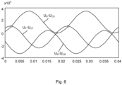
- Figure 6 illustrates an example of waveforms of respective voltages across each switch 1a, 1b and 1c.
- the voltage across the switch 1a of the first phase R is U R -U CR
- the voltage across the switch 1b of the second phase S is Us-Ucs
- the voltage across the switch 1c of the third phase T is U T -U CT .
- Such instances are marked with a small circle in the diagram of figure 6 .
Landscapes
- Engineering & Computer Science (AREA)
- Power Engineering (AREA)
- Driving Mechanisms And Operating Circuits Of Arc-Extinguishing High-Tension Switches (AREA)
- Inverter Devices (AREA)
Priority Applications (3)
| Application Number | Priority Date | Filing Date | Title |
|---|---|---|---|
| EP22216194.5A EP4391265A1 (de) | 2022-12-22 | 2022-12-22 | Reduzierung des einschaltstroms zu einer kondensatorbank |
| US18/534,998 US12562564B2 (en) | 2022-12-22 | 2023-12-11 | Reducing inrush current to a capacitor bank |
| CN202311721778.7A CN118249301A (zh) | 2022-12-22 | 2023-12-14 | 减少去往电容器组的涌入电流 |
Applications Claiming Priority (1)
| Application Number | Priority Date | Filing Date | Title |
|---|---|---|---|
| EP22216194.5A EP4391265A1 (de) | 2022-12-22 | 2022-12-22 | Reduzierung des einschaltstroms zu einer kondensatorbank |
Publications (1)
| Publication Number | Publication Date |
|---|---|
| EP4391265A1 true EP4391265A1 (de) | 2024-06-26 |
Family
ID=84569502
Family Applications (1)
| Application Number | Title | Priority Date | Filing Date |
|---|---|---|---|
| EP22216194.5A Pending EP4391265A1 (de) | 2022-12-22 | 2022-12-22 | Reduzierung des einschaltstroms zu einer kondensatorbank |
Country Status (3)
| Country | Link |
|---|---|
| US (1) | US12562564B2 (de) |
| EP (1) | EP4391265A1 (de) |
| CN (1) | CN118249301A (de) |
Citations (4)
| Publication number | Priority date | Publication date | Assignee | Title |
|---|---|---|---|---|
| EP0222727B1 (de) * | 1985-09-10 | 1989-07-26 | Sprecher Energie Österreich Gesellschaft m.b.H. | Einrichtung zum Minimieren von Netzrückwirkungen beim Ein- und Ausschalten von induktiven und kapazitiven Elementen im Hochspannungsnetz |
| WO2001050561A1 (en) * | 2000-01-03 | 2001-07-12 | Eaton Corporation | Modular, miniaturized switchgear |
| US20070253124A1 (en) * | 2006-05-01 | 2007-11-01 | Eaton Corporation | Circuit interrupter including point-on-wave controller and voltage sensors |
| EP3230998B1 (de) * | 2014-12-11 | 2018-12-05 | General Electric Technology GmbH | Verfahren zum betrieb kapazitiver lasten und vorrichtung zur durchführung des verfahrens |
Family Cites Families (7)
| Publication number | Priority date | Publication date | Assignee | Title |
|---|---|---|---|---|
| DE4425247A1 (de) | 1994-07-16 | 1996-01-18 | Fraunhofer Ges Forschung | Schaltvorrichtung für eine kondensatorbestückte Blindleistungskompensationseinrichtung |
| DE19639064C2 (de) | 1996-09-16 | 2001-05-31 | Eaw Relaistechnik Gmbh | Elektromagnetisch betätigtes, dreipolig symmetrisch aufgebautes Schütz |
| DE19803775C1 (de) | 1998-01-26 | 1999-07-15 | Eckehard Dr Ing Gebauer | Synchronisiert schaltendes ein- oder mehrpoliges Vakuumschütz |
| CA2298583C (en) | 1998-07-16 | 2004-08-31 | Mitsubishi Denki Kabushiki Kaisha | Synchronous switching apparatus for use with a multiple phase power sys tem |
| JP2000188044A (ja) | 1998-12-21 | 2000-07-04 | Mitsubishi Electric Corp | 位相制御開閉装置 |
| JP5547013B2 (ja) * | 2010-09-22 | 2014-07-09 | 株式会社東芝 | 突入電流抑制装置 |
| EP3358588A1 (de) * | 2017-02-02 | 2018-08-08 | ABB Schweiz AG | Dreipoliger leistungsschalter mit phasenspezifischer ansteuerung |
-
2022
- 2022-12-22 EP EP22216194.5A patent/EP4391265A1/de active Pending
-
2023
- 2023-12-11 US US18/534,998 patent/US12562564B2/en active Active
- 2023-12-14 CN CN202311721778.7A patent/CN118249301A/zh active Pending
Patent Citations (4)
| Publication number | Priority date | Publication date | Assignee | Title |
|---|---|---|---|---|
| EP0222727B1 (de) * | 1985-09-10 | 1989-07-26 | Sprecher Energie Österreich Gesellschaft m.b.H. | Einrichtung zum Minimieren von Netzrückwirkungen beim Ein- und Ausschalten von induktiven und kapazitiven Elementen im Hochspannungsnetz |
| WO2001050561A1 (en) * | 2000-01-03 | 2001-07-12 | Eaton Corporation | Modular, miniaturized switchgear |
| US20070253124A1 (en) * | 2006-05-01 | 2007-11-01 | Eaton Corporation | Circuit interrupter including point-on-wave controller and voltage sensors |
| EP3230998B1 (de) * | 2014-12-11 | 2018-12-05 | General Electric Technology GmbH | Verfahren zum betrieb kapazitiver lasten und vorrichtung zur durchführung des verfahrens |
Also Published As
| Publication number | Publication date |
|---|---|
| CN118249301A (zh) | 2024-06-25 |
| US12562564B2 (en) | 2026-02-24 |
| US20240213764A1 (en) | 2024-06-27 |
Similar Documents
| Publication | Publication Date | Title |
|---|---|---|
| US4405867A (en) | System for transferring a load between two power sources without interruption of power to the load | |
| EP3041016B1 (de) | Gleichstromleistungsschalter und ausschaltungsverfahren des gleichstromleistungsschalters | |
| MX2008000516A (es) | Dispositivo de arranque de motor electrico a base de sistema micro-electromecanico. | |
| EP2523205B1 (de) | Schaltung und Verfahren zur Unterbrechung des Stromflusses in einem Gleichstrompfad | |
| US10110057B2 (en) | Transfer switch apparatus and methods using transition time monitoring and adaptation | |
| EP3577670B1 (de) | Dreipoliger leistungsschalter mit phasenspezifischer ansteuerung | |
| US5635772A (en) | Method and apparatus for transferring between electrical power sources which adaptively blocks transfer until load voltage decays to safe value | |
| US3786337A (en) | Thyristors for effecting tap changing on transformers and including current limiting resistors and standby trigger system | |
| US3887860A (en) | Fuseless inverter | |
| MXPA96005115A (en) | Method and apparatus for transfer between sources of electrical energy that block adaptative transfer until the voltage of charge achieves a secure value | |
| EP4391265A1 (de) | Reduzierung des einschaltstroms zu einer kondensatorbank | |
| US10840042B2 (en) | Method of performing a circuit-breaking and closing operation | |
| JP4495030B2 (ja) | 開閉装置の閉極位相制御装置 | |
| EP0923801A1 (de) | Phasenüberwachung | |
| US11251599B2 (en) | DC circuit breaker | |
| US12603494B2 (en) | Reducing transformer inrush current | |
| EP4297214A1 (de) | Reduzieren des transformator-einschaltstroms | |
| EP4297215B1 (de) | Reduzieren des transformator-einschaltstroms | |
| EP2656363B1 (de) | Schaltanordnung | |
| EP1634311B1 (de) | Stromversorgung von Kondensatorlasten | |
| SU1117773A1 (ru) | Способ автоматического повторного включени трехфазной линии электропередачи | |
| AU2010366069A1 (en) | Switching arrangement | |
| SU1550441A1 (ru) | Способ определени наличи короткого замыкани и рассто ни до его места в электрической сети напр жением 6-10 кВ | |
| SU1144166A1 (ru) | Ограничитель дуговых перенапр жений | |
| SU612330A1 (ru) | Способ трехфазного автоматического повторного включени с контролем напр жени и улавливанием синхронизма линии электропередачи с шунтирующими реакторами |
Legal Events
| Date | Code | Title | Description |
|---|---|---|---|
| PUAI | Public reference made under article 153(3) epc to a published international application that has entered the european phase |
Free format text: ORIGINAL CODE: 0009012 |
|
| STAA | Information on the status of an ep patent application or granted ep patent |
Free format text: STATUS: THE APPLICATION HAS BEEN PUBLISHED |
|
| AK | Designated contracting states |
Kind code of ref document: A1 Designated state(s): AL AT BE BG CH CY CZ DE DK EE ES FI FR GB GR HR HU IE IS IT LI LT LU LV MC ME MK MT NL NO PL PT RO RS SE SI SK SM TR |
|
| STAA | Information on the status of an ep patent application or granted ep patent |
Free format text: STATUS: REQUEST FOR EXAMINATION WAS MADE |
|
| 17P | Request for examination filed |
Effective date: 20241121 |
|
| RBV | Designated contracting states (corrected) |
Designated state(s): AL AT BE BG CH CY CZ DE DK EE ES FI FR GB GR HR HU IE IS IT LI LT LU LV MC ME MK MT NL NO PL PT RO RS SE SI SK SM TR |