EP4393634A1 - Lötlegierung, lötkugel, lötvorform, lötpaste und lötverbindung - Google Patents
Lötlegierung, lötkugel, lötvorform, lötpaste und lötverbindung Download PDFInfo
- Publication number
- EP4393634A1 EP4393634A1 EP22876492.4A EP22876492A EP4393634A1 EP 4393634 A1 EP4393634 A1 EP 4393634A1 EP 22876492 A EP22876492 A EP 22876492A EP 4393634 A1 EP4393634 A1 EP 4393634A1
- Authority
- EP
- European Patent Office
- Prior art keywords
- solder
- good
- excellent excellent
- bal
- less
- Prior art date
- Legal status (The legal status is an assumption and is not a legal conclusion. Google has not performed a legal analysis and makes no representation as to the accuracy of the status listed.)
- Pending
Links
Images

Classifications
-
- B—PERFORMING OPERATIONS; TRANSPORTING
- B23—MACHINE TOOLS; METAL-WORKING NOT OTHERWISE PROVIDED FOR
- B23K—SOLDERING OR UNSOLDERING; WELDING; CLADDING OR PLATING BY SOLDERING OR WELDING; CUTTING BY APPLYING HEAT LOCALLY, e.g. FLAME CUTTING; WORKING BY LASER BEAM
- B23K35/00—Rods, electrodes, materials, or media, for use in soldering, welding, or cutting
- B23K35/02—Rods, electrodes, materials, or media, for use in soldering, welding, or cutting characterised by mechanical features, e.g. shape
- B23K35/0222—Rods, electrodes, materials, or media, for use in soldering, welding, or cutting characterised by mechanical features, e.g. shape for use in soldering or brazing
- B23K35/0244—Powders, particles or spheres; Preforms made therefrom
-
- B—PERFORMING OPERATIONS; TRANSPORTING
- B23—MACHINE TOOLS; METAL-WORKING NOT OTHERWISE PROVIDED FOR
- B23K—SOLDERING OR UNSOLDERING; WELDING; CLADDING OR PLATING BY SOLDERING OR WELDING; CUTTING BY APPLYING HEAT LOCALLY, e.g. FLAME CUTTING; WORKING BY LASER BEAM
- B23K35/00—Rods, electrodes, materials, or media, for use in soldering, welding, or cutting
- B23K35/22—Rods, electrodes, materials, or media, for use in soldering, welding, or cutting characterised by the composition or nature of the material
- B23K35/24—Selection of soldering or welding materials proper
- B23K35/26—Selection of soldering or welding materials proper with the principal constituent melting at less than 400°C
- B23K35/262—Sn as the principal constituent
-
- B—PERFORMING OPERATIONS; TRANSPORTING
- B23—MACHINE TOOLS; METAL-WORKING NOT OTHERWISE PROVIDED FOR
- B23K—SOLDERING OR UNSOLDERING; WELDING; CLADDING OR PLATING BY SOLDERING OR WELDING; CUTTING BY APPLYING HEAT LOCALLY, e.g. FLAME CUTTING; WORKING BY LASER BEAM
- B23K35/00—Rods, electrodes, materials, or media, for use in soldering, welding, or cutting
- B23K35/02—Rods, electrodes, materials, or media, for use in soldering, welding, or cutting characterised by mechanical features, e.g. shape
- B23K35/0222—Rods, electrodes, materials, or media, for use in soldering, welding, or cutting characterised by mechanical features, e.g. shape for use in soldering or brazing
- B23K35/0244—Powders, particles or spheres; Preforms made therefrom
- B23K35/025—Pastes, creams or slurries
-
- B—PERFORMING OPERATIONS; TRANSPORTING
- B23—MACHINE TOOLS; METAL-WORKING NOT OTHERWISE PROVIDED FOR
- B23K—SOLDERING OR UNSOLDERING; WELDING; CLADDING OR PLATING BY SOLDERING OR WELDING; CUTTING BY APPLYING HEAT LOCALLY, e.g. FLAME CUTTING; WORKING BY LASER BEAM
- B23K35/00—Rods, electrodes, materials, or media, for use in soldering, welding, or cutting
- B23K35/22—Rods, electrodes, materials, or media, for use in soldering, welding, or cutting characterised by the composition or nature of the material
- B23K35/24—Selection of soldering or welding materials proper
- B23K35/26—Selection of soldering or welding materials proper with the principal constituent melting at less than 400°C
-
- C—CHEMISTRY; METALLURGY
- C22—METALLURGY; FERROUS OR NON-FERROUS ALLOYS; TREATMENT OF ALLOYS OR NON-FERROUS METALS
- C22C—ALLOYS
- C22C13/00—Alloys based on tin
Definitions
- the present invention relates to a solder alloy, a solder ball, a solder preform, a solder paste, and a solder joint to be used for various electronic equipment.
- solder joints in which the solder joints are exposed to a harsh environment include, in addition to use for commercial-off-the-shelf electronic equipment, use for vehicle-mounted electronic equipment or industrial electronic equipment.
- a substrate of vehicle-mounted electronic equipment may be disposed in a position to be exposed to a high temperature, such as an engine room.
- a temperature as low as -40°C or less in a cold weather region depending on the use environment, a physical external force such as an impact may be applied to the electronic equipment.
- An object of the present invention is to provide a solder alloy, a solder ball, a solder preform, a solder paste, and a solder j oint, which have excellent wettability and high reliability by prevention of rupture of solder joints.
- the inventors intentionally focused on In that causes a volume change of the solder alloy. Depending on a content, In promotes solid-phase transformation between ⁇ Sn and ySn, and accordingly causes a volume change due to the solid-phase transformation. Then, the inventors examined a solder alloy with an increased content of In as described in Patent Document 1.
- the inventors examined contents of Cu, Sb, and Ni in detail. Further, the inventors focused on the fact that, at the time of a temperature rise of a solder joint in a cooling/heating cycle, when solid-phase transformation from ⁇ Sn to ⁇ Sn immediately occurs, the stress is quickly relaxed, and also examined the content of Ag in detail. As a result, the inventors found that a solder alloy with contents of Ag, Cu, Sb, In, and Ni as additive elements concurrently falling within predetermined ranges has excellent wettability, and prevents rupture of solder joints, and completed the present invention.
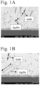
- Fig. 1 is sectional SEM photographs of solder alloys
- Fig. 1A illustrates that in Example 6
- Fig. 1B that in illustrates Comparative Example 3
- Fig. 1C illustrates that in Comparative Example 8.
- Ag can quickly relax the strain energy at the time of temperature rise by decreasing a temperature that causes phase transformation from ⁇ Sn to ySn, and prevent rupture of solder joints.
- Ag forms a network of Ag 3 Sn, and can improve the strength of the solder alloy itself.
- the Ag content is less than 1.0%, the temperature that causes phase transformation from ⁇ Sn to ⁇ Sn does not decrease and phase transformation does not occur, and rupture of solder joints cannot be prevented. Further, a fine Ag 3 Sn network is not formed, and the strength deteriorates.
- a lower limit of the Ag content is 1.0% or more, preferably 1.5% or more, and more preferably 2.0% or more.
- an Ag content of more than 3.7% causes crystallization of a coarse Ag 3 Sn primary crystal, and deteriorates the strength.
- An upper limit of the Ag content is 3.7% or less, preferably 3.0% or less, and more preferably 2.3% or less.
- Cu can improve the wettability of molten solder by suppressing an increase in liquidus-line temperature.
- the Cu content is less than 0.4% or more than 0.8%, the liquidus-line temperature increases, the fluidity at a joining temperature deteriorates, and accordingly, the wettability deteriorates.
- the Cu content is more than 0.8%, a compound of Cu and Sn precipitates, and an intermetallic compound formed at a joint interface becomes hard.
- a lower limit of the Cu content is 0.4% or more, preferably 0.5% or more.
- An upper limit of the Cu content is 0.8% or less, preferably 0.7% or less, and more preferably 0.6% or less.
- Sb can cause a fine InSb compound to crystallize and improve the strength of the solder alloy itself when Sb is added to the solder alloy with a predetermined content of In.
- the solid solubility limit of Sb to Sn changes in an operating temperature range including a room temperature, so that solid solution of Sb into Sn and Sb precipitation are repeated according to temperature changes.
- Sb forms a supersaturated solid solution in a high-temperature range, so that the solder alloy is improved in bulk strength due to solid solution strengthening. According to this, the liquidus-line temperature decreases, so that the wettability is improved.
- In When In reaches a transformation point in response to a temperature change, In causes gradual phase transformation from ⁇ Sn to ySn, and accordingly, the strain energy is relaxed, and a solder joint can be prevented from being ruptured.
- a solder joint was conventionally considered to easily rupture when its volume change was large in a cooling/heating cycle, in the present invention, by intentionally preparing the alloy composition so as to increase the volume change, a solder joint can be more effectively prevented from being ruptured than in the case of conventional solder alloys.
- the In content is less than 5.0%, solid-phase transformation of the Sn phase does not occur.
- a lower limit of the In content is 5.0% or more, preferably 6.00% or more, and more preferably 7.50%.
- the In content is more than 10.00%, the liquidus-line temperature excessively decreases, and solid-phase transformation of the Sn phase does not occur.
- An upper limit of the In content is 10.00% or less, and preferably 9.00% or less.
- Ni can strengthen a joint interface by blocking diffusion of Cu to Sn after soldering, suppressing growth of an intermetallic compound that precipitates at the joint interface, and suppressing coarsening of the intermetallic compound that precipitates at the joint interface.
- the joint interface cannot be strengthened.
- a lower limit of the Ni content is 0.01% or more, preferably 0.02% or more, and more preferably 0.03% or more.
- the Ni content is more than 0.06%, due to an increase in liquidus-line temperature, the wettability deteriorates.
- An upper limit of the Ni content is 0.06% or less, preferably 0.05% or less, and more preferably 0.04% or less.
- the balance of the solder alloy according to the present invention is Sn.
- unavoidable impurity may be contained. Even when unavoidable impurity is contained, it does not affect the above-described effects.
- Co is an optional element having the effects of suppressing growth of the intermetallic compound and refining the alloy structure.
- An upper limit of the Co content is preferably 0.100% or less, more preferably 0.050% or less, and further preferably 0.010% or less.
- a lower limit of the Co content is not particularly limited, from the viewpoint of refining the alloy structure, the lower limit is preferably 0.001% or more, more preferably 0.003% or more, further preferably 0.005% or more, still further preferably 0.006% or more, particularly preferably 0.007% or more, and most preferably 0.008% or more.
- Bi is an optional element that dissolves in the Sn phase and can improve the strength of the solder alloy. When an appropriate amount of Bi is added, the solder alloy may not embrittle but maintain high strength.
- An upper limit of the Bi content is preferably 5.0% or less, more preferably 1.0% or less, and further preferably 0.3% or less. Although a lower limit of the Bi content is not particularly limited, from the viewpoint of sufficiently obtaining solid solution strengthening, the lower limit needs to be 0.1% or more.
- the liquidus-line temperature can be adjusted to a more proper range.
- the liquidus-line temperature decreases as its content increases, and Cu, Sb, and Ni whose liquidus-line temperatures rise as their contents increase, are contained so as to maintain their balance.
- Cu, Sb, and Ni form an intermetallic compound whose melting point is higher than that of Sn, so that in order to obtain a proper liquidus-line temperature, it is preferable that their contents are comprehensively adjusted as well as the content of In.
- a lower limit of the relation (2) is preferably 251 or more, more preferably 300 or more, and particularly preferably 345 or more.
- An upper limit of the relation (2) is preferably 699 or less, more preferably 600 or less, and further preferably 500 or less.
- the solder alloy according to the present invention can be used as a solder ball.
- a solder ball according to the present invention is used to form bumps of electrodes and a substrate of a semiconductor package such as a BGA (Ball Grid Array).
- a diameter of the solder ball according to the present invention is preferably within a range of 1 to 1000 ⁇ m.
- the solder ball can be produced by a general solder ball production method.
- a shape of a solder preform according to the present invention is not particularly limited, and can be used in the form of a plate shape, a ring shape, a cylindrical shape, a ribbon shape, a square shape, a disc shape, a washer shape, a chip shape, and a wire shape, etc.
- the solder preform may internally contain high-melting-point metallic grains (for example, Ni grains and Cu grains, and an alloy powder mainly containing Ni and Cu) that have a melting point higher than that of the solder alloy and are easily wet with molten solder.
- the solder alloy according to the present invention can be used as solder paste.
- the solder paste is obtained by mixing a solder alloy powder with a small amount of flux and processing these in paste form.
- the solder alloy according to the present invention may be used as solder paste for mounting an electronic component to a printed circuit board by a reflow soldering method.
- the flux to be used for the solder paste may be either a water-soluble flux or a water-insoluble flux. Typically, a rosin-based flux as a rosin-based water-insoluble flux is used.
Landscapes
- Engineering & Computer Science (AREA)
- Mechanical Engineering (AREA)
- Chemical & Material Sciences (AREA)
- Materials Engineering (AREA)
- Metallurgy (AREA)
- Organic Chemistry (AREA)
- Electric Connection Of Electric Components To Printed Circuits (AREA)
Applications Claiming Priority (2)
| Application Number | Priority Date | Filing Date | Title |
|---|---|---|---|
| JP2021161531A JP7161133B1 (ja) | 2021-09-30 | 2021-09-30 | はんだ合金、はんだボール、はんだプリフォーム、はんだペースト及びはんだ継手 |
| PCT/JP2022/036552 WO2023054629A1 (ja) | 2021-09-30 | 2022-09-29 | はんだ合金、はんだボール、はんだプリフォーム、はんだペースト及びはんだ継手 |
Publications (2)
| Publication Number | Publication Date |
|---|---|
| EP4393634A1 true EP4393634A1 (de) | 2024-07-03 |
| EP4393634A4 EP4393634A4 (de) | 2025-07-09 |
Family
ID=83782320
Family Applications (1)
| Application Number | Title | Priority Date | Filing Date |
|---|---|---|---|
| EP22876492.4A Pending EP4393634A4 (de) | 2021-09-30 | 2022-09-29 | Lötlegierung, lötkugel, lötvorform, lötpaste und lötverbindung |
Country Status (8)
| Country | Link |
|---|---|
| US (1) | US20250058414A1 (de) |
| EP (1) | EP4393634A4 (de) |
| JP (1) | JP7161133B1 (de) |
| KR (1) | KR102786493B1 (de) |
| CN (1) | CN118043166B (de) |
| MX (1) | MX2024003975A (de) |
| TW (2) | TWI844972B (de) |
| WO (1) | WO2023054629A1 (de) |
Family Cites Families (20)
| Publication number | Priority date | Publication date | Assignee | Title |
|---|---|---|---|---|
| JPH037005A (ja) | 1989-06-02 | 1991-01-14 | Fuji Electric Co Ltd | 配電盤の引出形機器の落下防止装置 |
| JP2002086294A (ja) * | 2000-09-14 | 2002-03-26 | Nippon Steel Corp | 半田合金、半田ボールおよび半田バンプを有する電子部材 |
| JP2004188453A (ja) * | 2002-12-11 | 2004-07-08 | Harima Chem Inc | Sn系はんだ合金 |
| WO2014013632A1 (ja) | 2012-07-19 | 2014-01-23 | ハリマ化成株式会社 | はんだ合金、ソルダペーストおよび電子回路基板 |
| CN103341699A (zh) * | 2013-07-04 | 2013-10-09 | 浙江亚通焊材有限公司 | 一种取代锡铅钎料的Sn-In-Ag无铅钎料 |
| JP5730354B2 (ja) * | 2013-07-17 | 2015-06-10 | ハリマ化成株式会社 | はんだ組成物、ソルダペーストおよび電子回路基板 |
| AU2015254179B2 (en) * | 2014-04-30 | 2017-07-20 | Nihon Superior Co., Ltd. | Lead-free solder alloy |
| US9931716B2 (en) * | 2014-06-24 | 2018-04-03 | Harima Chemicals, Incorporated | Solder alloy, solder composition, solder paste, and electronic circuit board |
| US20160279741A1 (en) * | 2015-03-24 | 2016-09-29 | Tamura Corporation | Lead-free solder alloy, electronic circuit board, and electronic control device |
| JP6560272B2 (ja) * | 2017-01-31 | 2019-08-14 | 株式会社タムラ製作所 | ソルダペースト、電子回路基板及び電子制御装置 |
| BR112018068596A2 (pt) * | 2016-03-22 | 2019-02-12 | Tamura Corporation | liga de soldas sem chumbo, composição de fluxo, composição de pasta de solda, placa de circuito eletrônico, e controlador eletrônico |
| JP6745453B2 (ja) * | 2016-05-18 | 2020-08-26 | パナソニックIpマネジメント株式会社 | はんだ合金およびそれを用いた実装構造体 |
| JP6230737B1 (ja) * | 2017-03-10 | 2017-11-15 | 株式会社タムラ製作所 | 鉛フリーはんだ合金、ソルダペースト及び電子回路基板 |
| JP6349615B1 (ja) * | 2017-10-03 | 2018-07-04 | 株式会社弘輝 | はんだ合金、はんだ接合材料及び電子回路基板 |
| JP2019155467A (ja) * | 2018-03-16 | 2019-09-19 | 千住金属工業株式会社 | 鉛フリーはんだ合金 |
| CN112638574A (zh) * | 2018-08-31 | 2021-04-09 | 铟泰公司 | SnBi和SnIn焊锡合金 |
| CN108994480A (zh) * | 2018-10-10 | 2018-12-14 | 云南锡业锡材有限公司 | 一种SnBiAgCu高可靠性无铅焊料合金 |
| JP6624322B1 (ja) * | 2019-03-27 | 2019-12-25 | 千住金属工業株式会社 | はんだ合金、はんだボール、はんだプリフォーム、はんだペースト及びはんだ継手 |
| JP7089491B2 (ja) * | 2019-04-23 | 2022-06-22 | 株式会社タムラ製作所 | フラックス組成物、ソルダペースト及び電子回路基板 |
| TWI814081B (zh) * | 2019-09-02 | 2023-09-01 | 美商阿爾發金屬化工公司 | 高溫超高可靠性合金、其製造方法及其應用 |
-
2021
- 2021-09-30 JP JP2021161531A patent/JP7161133B1/ja active Active
-
2022
- 2022-09-29 WO PCT/JP2022/036552 patent/WO2023054629A1/ja not_active Ceased
- 2022-09-29 MX MX2024003975A patent/MX2024003975A/es unknown
- 2022-09-29 EP EP22876492.4A patent/EP4393634A4/de active Pending
- 2022-09-29 KR KR1020247013098A patent/KR102786493B1/ko active Active
- 2022-09-29 CN CN202280066205.2A patent/CN118043166B/zh active Active
- 2022-09-29 US US18/697,138 patent/US20250058414A1/en active Pending
- 2022-09-30 TW TW111137230A patent/TWI844972B/zh active
- 2022-09-30 TW TW113104128A patent/TWI845466B/zh active
Also Published As
| Publication number | Publication date |
|---|---|
| TW202421326A (zh) | 2024-06-01 |
| KR20240056780A (ko) | 2024-04-30 |
| CN118043166B (zh) | 2024-11-12 |
| TW202315698A (zh) | 2023-04-16 |
| US20250058414A1 (en) | 2025-02-20 |
| TWI844972B (zh) | 2024-06-11 |
| KR102786493B1 (ko) | 2025-03-28 |
| WO2023054629A1 (ja) | 2023-04-06 |
| CN118043166A (zh) | 2024-05-14 |
| EP4393634A4 (de) | 2025-07-09 |
| MX2024003975A (es) | 2024-04-29 |
| TWI845466B (zh) | 2024-06-11 |
| JP2023051074A (ja) | 2023-04-11 |
| JP7161133B1 (ja) | 2022-10-26 |
Similar Documents
| Publication | Publication Date | Title |
|---|---|---|
| CN111745321B (zh) | 软钎料合金、焊料球、软钎料预成型坯、焊膏和钎焊接头 | |
| EP2937432B1 (de) | Bleifreie messinglegierung | |
| EP4393635A1 (de) | Lötlegierung, lötkugel, lötvorform, lötpaste und lötverbindung | |
| CN115815871B (zh) | 软钎料合金、焊膏、软钎料预成型坯和钎焊接头 | |
| TWI645047B (zh) | 焊料合金、焊料球及焊接接頭 | |
| CN111683785B (zh) | 焊料合金、焊膏、焊球、带芯焊料及焊接接头 | |
| KR102672970B1 (ko) | 땜납 합금, 땜납 볼, 땜납 페이스트 및 솔더 조인트 | |
| EP4393634A1 (de) | Lötlegierung, lötkugel, lötvorform, lötpaste und lötverbindung | |
| EP4674561A1 (de) | Lötlegierung, lötkugel, lötvorform, lötverbindung und schaltung | |
| EP4667148A1 (de) | Lötlegierung, lötkugel, lötpaste und lötverbindung | |
| EP4169660B1 (de) | Lötlegierung, lötpaste, lötkugel, lötvorform und lötverbindung | |
| HK40104161B (zh) | 软釺料合金、焊料球、预成型软釺料、焊膏和釺焊接头 | |
| HK40104161A (zh) | 软釺料合金、焊料球、预成型软釺料、焊膏和釺焊接头 | |
| HK40103889A (zh) | 软釺料合金、焊料球、预成型软釺料、焊膏和釺焊接头 |
Legal Events
| Date | Code | Title | Description |
|---|---|---|---|
| STAA | Information on the status of an ep patent application or granted ep patent |
Free format text: STATUS: THE INTERNATIONAL PUBLICATION HAS BEEN MADE |
|
| PUAI | Public reference made under article 153(3) epc to a published international application that has entered the european phase |
Free format text: ORIGINAL CODE: 0009012 |
|
| STAA | Information on the status of an ep patent application or granted ep patent |
Free format text: STATUS: REQUEST FOR EXAMINATION WAS MADE |
|
| 17P | Request for examination filed |
Effective date: 20240328 |
|
| AK | Designated contracting states |
Kind code of ref document: A1 Designated state(s): AL AT BE BG CH CY CZ DE DK EE ES FI FR GB GR HR HU IE IS IT LI LT LU LV MC MK MT NL NO PL PT RO RS SE SI SK SM TR |
|
| DAV | Request for validation of the european patent (deleted) | ||
| DAX | Request for extension of the european patent (deleted) | ||
| A4 | Supplementary search report drawn up and despatched |
Effective date: 20250610 |
|
| RIC1 | Information provided on ipc code assigned before grant |
Ipc: C22C 13/00 20060101ALI20250603BHEP Ipc: B23K 35/02 20060101ALI20250603BHEP Ipc: B23K 35/26 20060101AFI20250603BHEP |