EP4394079A1 - Appareil et procédé de traitement de substrat - Google Patents
Appareil et procédé de traitement de substrat Download PDFInfo
- Publication number
- EP4394079A1 EP4394079A1 EP23806984.3A EP23806984A EP4394079A1 EP 4394079 A1 EP4394079 A1 EP 4394079A1 EP 23806984 A EP23806984 A EP 23806984A EP 4394079 A1 EP4394079 A1 EP 4394079A1
- Authority
- EP
- European Patent Office
- Prior art keywords
- pipelines
- source
- carrier gas
- cavity
- gas
- Prior art date
- Legal status (The legal status is an assumption and is not a legal conclusion. Google has not performed a legal analysis and makes no representation as to the accuracy of the status listed.)
- Granted
Links
Images




Classifications
-
- C—CHEMISTRY; METALLURGY
- C23—COATING METALLIC MATERIAL; COATING MATERIAL WITH METALLIC MATERIAL; CHEMICAL SURFACE TREATMENT; DIFFUSION TREATMENT OF METALLIC MATERIAL; COATING BY VACUUM EVAPORATION, BY SPUTTERING, BY ION IMPLANTATION OR BY CHEMICAL VAPOUR DEPOSITION, IN GENERAL; INHIBITING CORROSION OF METALLIC MATERIAL OR INCRUSTATION IN GENERAL
- C23C—COATING METALLIC MATERIAL; COATING MATERIAL WITH METALLIC MATERIAL; SURFACE TREATMENT OF METALLIC MATERIAL BY DIFFUSION INTO THE SURFACE, BY CHEMICAL CONVERSION OR SUBSTITUTION; COATING BY VACUUM EVAPORATION, BY SPUTTERING, BY ION IMPLANTATION OR BY CHEMICAL VAPOUR DEPOSITION, IN GENERAL
- C23C16/00—Chemical coating by decomposition of gaseous compounds, without leaving reaction products of surface material in the coating, i.e. chemical vapour deposition [CVD] processes
- C23C16/44—Chemical coating by decomposition of gaseous compounds, without leaving reaction products of surface material in the coating, i.e. chemical vapour deposition [CVD] processes characterised by the method of coating
- C23C16/455—Chemical coating by decomposition of gaseous compounds, without leaving reaction products of surface material in the coating, i.e. chemical vapour deposition [CVD] processes characterised by the method of coating characterised by the method used for introducing gases into reaction chamber or for modifying gas flows in reaction chamber
- C23C16/45523—Pulsed gas flow or change of composition over time
- C23C16/45525—Atomic layer deposition [ALD]
- C23C16/45544—Atomic layer deposition [ALD] characterized by the apparatus
-
- C—CHEMISTRY; METALLURGY
- C23—COATING METALLIC MATERIAL; COATING MATERIAL WITH METALLIC MATERIAL; CHEMICAL SURFACE TREATMENT; DIFFUSION TREATMENT OF METALLIC MATERIAL; COATING BY VACUUM EVAPORATION, BY SPUTTERING, BY ION IMPLANTATION OR BY CHEMICAL VAPOUR DEPOSITION, IN GENERAL; INHIBITING CORROSION OF METALLIC MATERIAL OR INCRUSTATION IN GENERAL
- C23C—COATING METALLIC MATERIAL; COATING MATERIAL WITH METALLIC MATERIAL; SURFACE TREATMENT OF METALLIC MATERIAL BY DIFFUSION INTO THE SURFACE, BY CHEMICAL CONVERSION OR SUBSTITUTION; COATING BY VACUUM EVAPORATION, BY SPUTTERING, BY ION IMPLANTATION OR BY CHEMICAL VAPOUR DEPOSITION, IN GENERAL
- C23C16/00—Chemical coating by decomposition of gaseous compounds, without leaving reaction products of surface material in the coating, i.e. chemical vapour deposition [CVD] processes
- C23C16/22—Chemical coating by decomposition of gaseous compounds, without leaving reaction products of surface material in the coating, i.e. chemical vapour deposition [CVD] processes characterised by the deposition of inorganic material, other than metallic material
- C23C16/30—Deposition of compounds, mixtures or solid solutions, e.g. borides, carbides, nitrides
- C23C16/34—Nitrides
- C23C16/345—Silicon nitride
-
- C—CHEMISTRY; METALLURGY
- C23—COATING METALLIC MATERIAL; COATING MATERIAL WITH METALLIC MATERIAL; CHEMICAL SURFACE TREATMENT; DIFFUSION TREATMENT OF METALLIC MATERIAL; COATING BY VACUUM EVAPORATION, BY SPUTTERING, BY ION IMPLANTATION OR BY CHEMICAL VAPOUR DEPOSITION, IN GENERAL; INHIBITING CORROSION OF METALLIC MATERIAL OR INCRUSTATION IN GENERAL
- C23C—COATING METALLIC MATERIAL; COATING MATERIAL WITH METALLIC MATERIAL; SURFACE TREATMENT OF METALLIC MATERIAL BY DIFFUSION INTO THE SURFACE, BY CHEMICAL CONVERSION OR SUBSTITUTION; COATING BY VACUUM EVAPORATION, BY SPUTTERING, BY ION IMPLANTATION OR BY CHEMICAL VAPOUR DEPOSITION, IN GENERAL
- C23C16/00—Chemical coating by decomposition of gaseous compounds, without leaving reaction products of surface material in the coating, i.e. chemical vapour deposition [CVD] processes
- C23C16/22—Chemical coating by decomposition of gaseous compounds, without leaving reaction products of surface material in the coating, i.e. chemical vapour deposition [CVD] processes characterised by the deposition of inorganic material, other than metallic material
- C23C16/30—Deposition of compounds, mixtures or solid solutions, e.g. borides, carbides, nitrides
- C23C16/40—Oxides
-
- C—CHEMISTRY; METALLURGY
- C23—COATING METALLIC MATERIAL; COATING MATERIAL WITH METALLIC MATERIAL; CHEMICAL SURFACE TREATMENT; DIFFUSION TREATMENT OF METALLIC MATERIAL; COATING BY VACUUM EVAPORATION, BY SPUTTERING, BY ION IMPLANTATION OR BY CHEMICAL VAPOUR DEPOSITION, IN GENERAL; INHIBITING CORROSION OF METALLIC MATERIAL OR INCRUSTATION IN GENERAL
- C23C—COATING METALLIC MATERIAL; COATING MATERIAL WITH METALLIC MATERIAL; SURFACE TREATMENT OF METALLIC MATERIAL BY DIFFUSION INTO THE SURFACE, BY CHEMICAL CONVERSION OR SUBSTITUTION; COATING BY VACUUM EVAPORATION, BY SPUTTERING, BY ION IMPLANTATION OR BY CHEMICAL VAPOUR DEPOSITION, IN GENERAL
- C23C16/00—Chemical coating by decomposition of gaseous compounds, without leaving reaction products of surface material in the coating, i.e. chemical vapour deposition [CVD] processes
- C23C16/22—Chemical coating by decomposition of gaseous compounds, without leaving reaction products of surface material in the coating, i.e. chemical vapour deposition [CVD] processes characterised by the deposition of inorganic material, other than metallic material
- C23C16/30—Deposition of compounds, mixtures or solid solutions, e.g. borides, carbides, nitrides
- C23C16/40—Oxides
- C23C16/401—Oxides containing silicon
-
- C—CHEMISTRY; METALLURGY
- C23—COATING METALLIC MATERIAL; COATING MATERIAL WITH METALLIC MATERIAL; CHEMICAL SURFACE TREATMENT; DIFFUSION TREATMENT OF METALLIC MATERIAL; COATING BY VACUUM EVAPORATION, BY SPUTTERING, BY ION IMPLANTATION OR BY CHEMICAL VAPOUR DEPOSITION, IN GENERAL; INHIBITING CORROSION OF METALLIC MATERIAL OR INCRUSTATION IN GENERAL
- C23C—COATING METALLIC MATERIAL; COATING MATERIAL WITH METALLIC MATERIAL; SURFACE TREATMENT OF METALLIC MATERIAL BY DIFFUSION INTO THE SURFACE, BY CHEMICAL CONVERSION OR SUBSTITUTION; COATING BY VACUUM EVAPORATION, BY SPUTTERING, BY ION IMPLANTATION OR BY CHEMICAL VAPOUR DEPOSITION, IN GENERAL
- C23C16/00—Chemical coating by decomposition of gaseous compounds, without leaving reaction products of surface material in the coating, i.e. chemical vapour deposition [CVD] processes
- C23C16/22—Chemical coating by decomposition of gaseous compounds, without leaving reaction products of surface material in the coating, i.e. chemical vapour deposition [CVD] processes characterised by the deposition of inorganic material, other than metallic material
- C23C16/30—Deposition of compounds, mixtures or solid solutions, e.g. borides, carbides, nitrides
- C23C16/40—Oxides
- C23C16/403—Oxides of aluminium, magnesium or beryllium
-
- C—CHEMISTRY; METALLURGY
- C23—COATING METALLIC MATERIAL; COATING MATERIAL WITH METALLIC MATERIAL; CHEMICAL SURFACE TREATMENT; DIFFUSION TREATMENT OF METALLIC MATERIAL; COATING BY VACUUM EVAPORATION, BY SPUTTERING, BY ION IMPLANTATION OR BY CHEMICAL VAPOUR DEPOSITION, IN GENERAL; INHIBITING CORROSION OF METALLIC MATERIAL OR INCRUSTATION IN GENERAL
- C23C—COATING METALLIC MATERIAL; COATING MATERIAL WITH METALLIC MATERIAL; SURFACE TREATMENT OF METALLIC MATERIAL BY DIFFUSION INTO THE SURFACE, BY CHEMICAL CONVERSION OR SUBSTITUTION; COATING BY VACUUM EVAPORATION, BY SPUTTERING, BY ION IMPLANTATION OR BY CHEMICAL VAPOUR DEPOSITION, IN GENERAL
- C23C16/00—Chemical coating by decomposition of gaseous compounds, without leaving reaction products of surface material in the coating, i.e. chemical vapour deposition [CVD] processes
- C23C16/22—Chemical coating by decomposition of gaseous compounds, without leaving reaction products of surface material in the coating, i.e. chemical vapour deposition [CVD] processes characterised by the deposition of inorganic material, other than metallic material
- C23C16/30—Deposition of compounds, mixtures or solid solutions, e.g. borides, carbides, nitrides
- C23C16/40—Oxides
- C23C16/405—Oxides of refractory metals or yttrium
-
- C—CHEMISTRY; METALLURGY
- C23—COATING METALLIC MATERIAL; COATING MATERIAL WITH METALLIC MATERIAL; CHEMICAL SURFACE TREATMENT; DIFFUSION TREATMENT OF METALLIC MATERIAL; COATING BY VACUUM EVAPORATION, BY SPUTTERING, BY ION IMPLANTATION OR BY CHEMICAL VAPOUR DEPOSITION, IN GENERAL; INHIBITING CORROSION OF METALLIC MATERIAL OR INCRUSTATION IN GENERAL
- C23C—COATING METALLIC MATERIAL; COATING MATERIAL WITH METALLIC MATERIAL; SURFACE TREATMENT OF METALLIC MATERIAL BY DIFFUSION INTO THE SURFACE, BY CHEMICAL CONVERSION OR SUBSTITUTION; COATING BY VACUUM EVAPORATION, BY SPUTTERING, BY ION IMPLANTATION OR BY CHEMICAL VAPOUR DEPOSITION, IN GENERAL
- C23C16/00—Chemical coating by decomposition of gaseous compounds, without leaving reaction products of surface material in the coating, i.e. chemical vapour deposition [CVD] processes
- C23C16/44—Chemical coating by decomposition of gaseous compounds, without leaving reaction products of surface material in the coating, i.e. chemical vapour deposition [CVD] processes characterised by the method of coating
- C23C16/4401—Means for minimising impurities, e.g. dust, moisture or residual gas, in the reaction chamber
- C23C16/4405—Cleaning of reactor or parts inside the reactor by using reactive gases
-
- C—CHEMISTRY; METALLURGY
- C23—COATING METALLIC MATERIAL; COATING MATERIAL WITH METALLIC MATERIAL; CHEMICAL SURFACE TREATMENT; DIFFUSION TREATMENT OF METALLIC MATERIAL; COATING BY VACUUM EVAPORATION, BY SPUTTERING, BY ION IMPLANTATION OR BY CHEMICAL VAPOUR DEPOSITION, IN GENERAL; INHIBITING CORROSION OF METALLIC MATERIAL OR INCRUSTATION IN GENERAL
- C23C—COATING METALLIC MATERIAL; COATING MATERIAL WITH METALLIC MATERIAL; SURFACE TREATMENT OF METALLIC MATERIAL BY DIFFUSION INTO THE SURFACE, BY CHEMICAL CONVERSION OR SUBSTITUTION; COATING BY VACUUM EVAPORATION, BY SPUTTERING, BY ION IMPLANTATION OR BY CHEMICAL VAPOUR DEPOSITION, IN GENERAL
- C23C16/00—Chemical coating by decomposition of gaseous compounds, without leaving reaction products of surface material in the coating, i.e. chemical vapour deposition [CVD] processes
- C23C16/44—Chemical coating by decomposition of gaseous compounds, without leaving reaction products of surface material in the coating, i.e. chemical vapour deposition [CVD] processes characterised by the method of coating
- C23C16/4401—Means for minimising impurities, e.g. dust, moisture or residual gas, in the reaction chamber
- C23C16/4408—Means for minimising impurities, e.g. dust, moisture or residual gas, in the reaction chamber by purging residual gases from the reaction chamber or gas lines
-
- C—CHEMISTRY; METALLURGY
- C23—COATING METALLIC MATERIAL; COATING MATERIAL WITH METALLIC MATERIAL; CHEMICAL SURFACE TREATMENT; DIFFUSION TREATMENT OF METALLIC MATERIAL; COATING BY VACUUM EVAPORATION, BY SPUTTERING, BY ION IMPLANTATION OR BY CHEMICAL VAPOUR DEPOSITION, IN GENERAL; INHIBITING CORROSION OF METALLIC MATERIAL OR INCRUSTATION IN GENERAL
- C23C—COATING METALLIC MATERIAL; COATING MATERIAL WITH METALLIC MATERIAL; SURFACE TREATMENT OF METALLIC MATERIAL BY DIFFUSION INTO THE SURFACE, BY CHEMICAL CONVERSION OR SUBSTITUTION; COATING BY VACUUM EVAPORATION, BY SPUTTERING, BY ION IMPLANTATION OR BY CHEMICAL VAPOUR DEPOSITION, IN GENERAL
- C23C16/00—Chemical coating by decomposition of gaseous compounds, without leaving reaction products of surface material in the coating, i.e. chemical vapour deposition [CVD] processes
- C23C16/44—Chemical coating by decomposition of gaseous compounds, without leaving reaction products of surface material in the coating, i.e. chemical vapour deposition [CVD] processes characterised by the method of coating
- C23C16/4412—Details relating to the exhausts, e.g. pumps, filters, scrubbers, particle traps
-
- C—CHEMISTRY; METALLURGY
- C23—COATING METALLIC MATERIAL; COATING MATERIAL WITH METALLIC MATERIAL; CHEMICAL SURFACE TREATMENT; DIFFUSION TREATMENT OF METALLIC MATERIAL; COATING BY VACUUM EVAPORATION, BY SPUTTERING, BY ION IMPLANTATION OR BY CHEMICAL VAPOUR DEPOSITION, IN GENERAL; INHIBITING CORROSION OF METALLIC MATERIAL OR INCRUSTATION IN GENERAL
- C23C—COATING METALLIC MATERIAL; COATING MATERIAL WITH METALLIC MATERIAL; SURFACE TREATMENT OF METALLIC MATERIAL BY DIFFUSION INTO THE SURFACE, BY CHEMICAL CONVERSION OR SUBSTITUTION; COATING BY VACUUM EVAPORATION, BY SPUTTERING, BY ION IMPLANTATION OR BY CHEMICAL VAPOUR DEPOSITION, IN GENERAL
- C23C16/00—Chemical coating by decomposition of gaseous compounds, without leaving reaction products of surface material in the coating, i.e. chemical vapour deposition [CVD] processes
- C23C16/44—Chemical coating by decomposition of gaseous compounds, without leaving reaction products of surface material in the coating, i.e. chemical vapour deposition [CVD] processes characterised by the method of coating
- C23C16/448—Chemical coating by decomposition of gaseous compounds, without leaving reaction products of surface material in the coating, i.e. chemical vapour deposition [CVD] processes characterised by the method of coating characterised by the method used for generating reactive gas streams, e.g. by evaporation or sublimation of precursor materials
- C23C16/4481—Chemical coating by decomposition of gaseous compounds, without leaving reaction products of surface material in the coating, i.e. chemical vapour deposition [CVD] processes characterised by the method of coating characterised by the method used for generating reactive gas streams, e.g. by evaporation or sublimation of precursor materials by evaporation using carrier gas in contact with the source material
-
- C—CHEMISTRY; METALLURGY
- C23—COATING METALLIC MATERIAL; COATING MATERIAL WITH METALLIC MATERIAL; CHEMICAL SURFACE TREATMENT; DIFFUSION TREATMENT OF METALLIC MATERIAL; COATING BY VACUUM EVAPORATION, BY SPUTTERING, BY ION IMPLANTATION OR BY CHEMICAL VAPOUR DEPOSITION, IN GENERAL; INHIBITING CORROSION OF METALLIC MATERIAL OR INCRUSTATION IN GENERAL
- C23C—COATING METALLIC MATERIAL; COATING MATERIAL WITH METALLIC MATERIAL; SURFACE TREATMENT OF METALLIC MATERIAL BY DIFFUSION INTO THE SURFACE, BY CHEMICAL CONVERSION OR SUBSTITUTION; COATING BY VACUUM EVAPORATION, BY SPUTTERING, BY ION IMPLANTATION OR BY CHEMICAL VAPOUR DEPOSITION, IN GENERAL
- C23C16/00—Chemical coating by decomposition of gaseous compounds, without leaving reaction products of surface material in the coating, i.e. chemical vapour deposition [CVD] processes
- C23C16/44—Chemical coating by decomposition of gaseous compounds, without leaving reaction products of surface material in the coating, i.e. chemical vapour deposition [CVD] processes characterised by the method of coating
- C23C16/455—Chemical coating by decomposition of gaseous compounds, without leaving reaction products of surface material in the coating, i.e. chemical vapour deposition [CVD] processes characterised by the method of coating characterised by the method used for introducing gases into reaction chamber or for modifying gas flows in reaction chamber
-
- C—CHEMISTRY; METALLURGY
- C23—COATING METALLIC MATERIAL; COATING MATERIAL WITH METALLIC MATERIAL; CHEMICAL SURFACE TREATMENT; DIFFUSION TREATMENT OF METALLIC MATERIAL; COATING BY VACUUM EVAPORATION, BY SPUTTERING, BY ION IMPLANTATION OR BY CHEMICAL VAPOUR DEPOSITION, IN GENERAL; INHIBITING CORROSION OF METALLIC MATERIAL OR INCRUSTATION IN GENERAL
- C23C—COATING METALLIC MATERIAL; COATING MATERIAL WITH METALLIC MATERIAL; SURFACE TREATMENT OF METALLIC MATERIAL BY DIFFUSION INTO THE SURFACE, BY CHEMICAL CONVERSION OR SUBSTITUTION; COATING BY VACUUM EVAPORATION, BY SPUTTERING, BY ION IMPLANTATION OR BY CHEMICAL VAPOUR DEPOSITION, IN GENERAL
- C23C16/00—Chemical coating by decomposition of gaseous compounds, without leaving reaction products of surface material in the coating, i.e. chemical vapour deposition [CVD] processes
- C23C16/44—Chemical coating by decomposition of gaseous compounds, without leaving reaction products of surface material in the coating, i.e. chemical vapour deposition [CVD] processes characterised by the method of coating
- C23C16/455—Chemical coating by decomposition of gaseous compounds, without leaving reaction products of surface material in the coating, i.e. chemical vapour deposition [CVD] processes characterised by the method of coating characterised by the method used for introducing gases into reaction chamber or for modifying gas flows in reaction chamber
- C23C16/45523—Pulsed gas flow or change of composition over time
- C23C16/45525—Atomic layer deposition [ALD]
- C23C16/45527—Atomic layer deposition [ALD] characterized by the ALD cycle, e.g. different flows or temperatures during half-reactions, unusual pulsing sequence, use of precursor mixtures or auxiliary reactants or activations
-
- C—CHEMISTRY; METALLURGY
- C23—COATING METALLIC MATERIAL; COATING MATERIAL WITH METALLIC MATERIAL; CHEMICAL SURFACE TREATMENT; DIFFUSION TREATMENT OF METALLIC MATERIAL; COATING BY VACUUM EVAPORATION, BY SPUTTERING, BY ION IMPLANTATION OR BY CHEMICAL VAPOUR DEPOSITION, IN GENERAL; INHIBITING CORROSION OF METALLIC MATERIAL OR INCRUSTATION IN GENERAL
- C23C—COATING METALLIC MATERIAL; COATING MATERIAL WITH METALLIC MATERIAL; SURFACE TREATMENT OF METALLIC MATERIAL BY DIFFUSION INTO THE SURFACE, BY CHEMICAL CONVERSION OR SUBSTITUTION; COATING BY VACUUM EVAPORATION, BY SPUTTERING, BY ION IMPLANTATION OR BY CHEMICAL VAPOUR DEPOSITION, IN GENERAL
- C23C16/00—Chemical coating by decomposition of gaseous compounds, without leaving reaction products of surface material in the coating, i.e. chemical vapour deposition [CVD] processes
- C23C16/44—Chemical coating by decomposition of gaseous compounds, without leaving reaction products of surface material in the coating, i.e. chemical vapour deposition [CVD] processes characterised by the method of coating
- C23C16/455—Chemical coating by decomposition of gaseous compounds, without leaving reaction products of surface material in the coating, i.e. chemical vapour deposition [CVD] processes characterised by the method of coating characterised by the method used for introducing gases into reaction chamber or for modifying gas flows in reaction chamber
- C23C16/45561—Gas plumbing upstream of the reaction chamber
-
- C—CHEMISTRY; METALLURGY
- C23—COATING METALLIC MATERIAL; COATING MATERIAL WITH METALLIC MATERIAL; CHEMICAL SURFACE TREATMENT; DIFFUSION TREATMENT OF METALLIC MATERIAL; COATING BY VACUUM EVAPORATION, BY SPUTTERING, BY ION IMPLANTATION OR BY CHEMICAL VAPOUR DEPOSITION, IN GENERAL; INHIBITING CORROSION OF METALLIC MATERIAL OR INCRUSTATION IN GENERAL
- C23C—COATING METALLIC MATERIAL; COATING MATERIAL WITH METALLIC MATERIAL; SURFACE TREATMENT OF METALLIC MATERIAL BY DIFFUSION INTO THE SURFACE, BY CHEMICAL CONVERSION OR SUBSTITUTION; COATING BY VACUUM EVAPORATION, BY SPUTTERING, BY ION IMPLANTATION OR BY CHEMICAL VAPOUR DEPOSITION, IN GENERAL
- C23C16/00—Chemical coating by decomposition of gaseous compounds, without leaving reaction products of surface material in the coating, i.e. chemical vapour deposition [CVD] processes
- C23C16/44—Chemical coating by decomposition of gaseous compounds, without leaving reaction products of surface material in the coating, i.e. chemical vapour deposition [CVD] processes characterised by the method of coating
- C23C16/46—Chemical coating by decomposition of gaseous compounds, without leaving reaction products of surface material in the coating, i.e. chemical vapour deposition [CVD] processes characterised by the method of coating characterised by the method used for heating the substrate
-
- C—CHEMISTRY; METALLURGY
- C23—COATING METALLIC MATERIAL; COATING MATERIAL WITH METALLIC MATERIAL; CHEMICAL SURFACE TREATMENT; DIFFUSION TREATMENT OF METALLIC MATERIAL; COATING BY VACUUM EVAPORATION, BY SPUTTERING, BY ION IMPLANTATION OR BY CHEMICAL VAPOUR DEPOSITION, IN GENERAL; INHIBITING CORROSION OF METALLIC MATERIAL OR INCRUSTATION IN GENERAL
- C23C—COATING METALLIC MATERIAL; COATING MATERIAL WITH METALLIC MATERIAL; SURFACE TREATMENT OF METALLIC MATERIAL BY DIFFUSION INTO THE SURFACE, BY CHEMICAL CONVERSION OR SUBSTITUTION; COATING BY VACUUM EVAPORATION, BY SPUTTERING, BY ION IMPLANTATION OR BY CHEMICAL VAPOUR DEPOSITION, IN GENERAL
- C23C16/00—Chemical coating by decomposition of gaseous compounds, without leaving reaction products of surface material in the coating, i.e. chemical vapour deposition [CVD] processes
- C23C16/44—Chemical coating by decomposition of gaseous compounds, without leaving reaction products of surface material in the coating, i.e. chemical vapour deposition [CVD] processes characterised by the method of coating
- C23C16/50—Chemical coating by decomposition of gaseous compounds, without leaving reaction products of surface material in the coating, i.e. chemical vapour deposition [CVD] processes characterised by the method of coating using electric discharges
-
- C—CHEMISTRY; METALLURGY
- C23—COATING METALLIC MATERIAL; COATING MATERIAL WITH METALLIC MATERIAL; CHEMICAL SURFACE TREATMENT; DIFFUSION TREATMENT OF METALLIC MATERIAL; COATING BY VACUUM EVAPORATION, BY SPUTTERING, BY ION IMPLANTATION OR BY CHEMICAL VAPOUR DEPOSITION, IN GENERAL; INHIBITING CORROSION OF METALLIC MATERIAL OR INCRUSTATION IN GENERAL
- C23C—COATING METALLIC MATERIAL; COATING MATERIAL WITH METALLIC MATERIAL; SURFACE TREATMENT OF METALLIC MATERIAL BY DIFFUSION INTO THE SURFACE, BY CHEMICAL CONVERSION OR SUBSTITUTION; COATING BY VACUUM EVAPORATION, BY SPUTTERING, BY ION IMPLANTATION OR BY CHEMICAL VAPOUR DEPOSITION, IN GENERAL
- C23C16/00—Chemical coating by decomposition of gaseous compounds, without leaving reaction products of surface material in the coating, i.e. chemical vapour deposition [CVD] processes
- C23C16/44—Chemical coating by decomposition of gaseous compounds, without leaving reaction products of surface material in the coating, i.e. chemical vapour deposition [CVD] processes characterised by the method of coating
- C23C16/52—Controlling or regulating the coating process
-
- C—CHEMISTRY; METALLURGY
- C23—COATING METALLIC MATERIAL; COATING MATERIAL WITH METALLIC MATERIAL; CHEMICAL SURFACE TREATMENT; DIFFUSION TREATMENT OF METALLIC MATERIAL; COATING BY VACUUM EVAPORATION, BY SPUTTERING, BY ION IMPLANTATION OR BY CHEMICAL VAPOUR DEPOSITION, IN GENERAL; INHIBITING CORROSION OF METALLIC MATERIAL OR INCRUSTATION IN GENERAL
- C23C—COATING METALLIC MATERIAL; COATING MATERIAL WITH METALLIC MATERIAL; SURFACE TREATMENT OF METALLIC MATERIAL BY DIFFUSION INTO THE SURFACE, BY CHEMICAL CONVERSION OR SUBSTITUTION; COATING BY VACUUM EVAPORATION, BY SPUTTERING, BY ION IMPLANTATION OR BY CHEMICAL VAPOUR DEPOSITION, IN GENERAL
- C23C16/00—Chemical coating by decomposition of gaseous compounds, without leaving reaction products of surface material in the coating, i.e. chemical vapour deposition [CVD] processes
- C23C16/44—Chemical coating by decomposition of gaseous compounds, without leaving reaction products of surface material in the coating, i.e. chemical vapour deposition [CVD] processes characterised by the method of coating
- C23C16/54—Apparatus specially adapted for continuous coating
-
- H—ELECTRICITY
- H01—ELECTRIC ELEMENTS
- H01J—ELECTRIC DISCHARGE TUBES OR DISCHARGE LAMPS
- H01J37/00—Discharge tubes with provision for introducing objects or material to be exposed to the discharge, e.g. for the purpose of examination or processing thereof
- H01J37/32—Gas-filled discharge tubes
-
- H—ELECTRICITY
- H10—SEMICONDUCTOR DEVICES; ELECTRIC SOLID-STATE DEVICES NOT OTHERWISE PROVIDED FOR
- H10F—INORGANIC SEMICONDUCTOR DEVICES SENSITIVE TO INFRARED RADIATION, LIGHT, ELECTROMAGNETIC RADIATION OF SHORTER WAVELENGTH OR CORPUSCULAR RADIATION
- H10F71/00—Manufacture or treatment of devices covered by this subclass
-
- H—ELECTRICITY
- H10—SEMICONDUCTOR DEVICES; ELECTRIC SOLID-STATE DEVICES NOT OTHERWISE PROVIDED FOR
- H10P—GENERIC PROCESSES OR APPARATUS FOR THE MANUFACTURE OR TREATMENT OF DEVICES COVERED BY CLASS H10
- H10P14/00—Formation of materials, e.g. in the shape of layers or pillars
- H10P14/60—Formation of materials, e.g. in the shape of layers or pillars of insulating materials
- H10P14/63—Formation of materials, e.g. in the shape of layers or pillars of insulating materials characterised by the formation processes
- H10P14/6326—Deposition processes
- H10P14/6328—Deposition from the gas or vapour phase
- H10P14/6334—Deposition from the gas or vapour phase using decomposition or reaction of gaseous or vapour phase compounds, i.e. chemical vapour deposition
- H10P14/6336—Deposition from the gas or vapour phase using decomposition or reaction of gaseous or vapour phase compounds, i.e. chemical vapour deposition in the presence of a plasma [PECVD]
-
- H—ELECTRICITY
- H10—SEMICONDUCTOR DEVICES; ELECTRIC SOLID-STATE DEVICES NOT OTHERWISE PROVIDED FOR
- H10P—GENERIC PROCESSES OR APPARATUS FOR THE MANUFACTURE OR TREATMENT OF DEVICES COVERED BY CLASS H10
- H10P14/00—Formation of materials, e.g. in the shape of layers or pillars
- H10P14/60—Formation of materials, e.g. in the shape of layers or pillars of insulating materials
- H10P14/63—Formation of materials, e.g. in the shape of layers or pillars of insulating materials characterised by the formation processes
- H10P14/6326—Deposition processes
- H10P14/6328—Deposition from the gas or vapour phase
- H10P14/6334—Deposition from the gas or vapour phase using decomposition or reaction of gaseous or vapour phase compounds, i.e. chemical vapour deposition
- H10P14/6339—Deposition from the gas or vapour phase using decomposition or reaction of gaseous or vapour phase compounds, i.e. chemical vapour deposition deposition by cyclic CVD, e.g. ALD, ALE or pulsed CVD
-
- H—ELECTRICITY
- H10—SEMICONDUCTOR DEVICES; ELECTRIC SOLID-STATE DEVICES NOT OTHERWISE PROVIDED FOR
- H10P—GENERIC PROCESSES OR APPARATUS FOR THE MANUFACTURE OR TREATMENT OF DEVICES COVERED BY CLASS H10
- H10P14/00—Formation of materials, e.g. in the shape of layers or pillars
- H10P14/60—Formation of materials, e.g. in the shape of layers or pillars of insulating materials
- H10P14/66—Formation of materials, e.g. in the shape of layers or pillars of insulating materials characterised by the type of materials
- H10P14/668—Formation of materials, e.g. in the shape of layers or pillars of insulating materials characterised by the type of materials the materials being characterised by the deposition precursor materials
- H10P14/6681—Formation of materials, e.g. in the shape of layers or pillars of insulating materials characterised by the type of materials the materials being characterised by the deposition precursor materials the precursor containing a compound comprising Si
- H10P14/6682—Formation of materials, e.g. in the shape of layers or pillars of insulating materials characterised by the type of materials the materials being characterised by the deposition precursor materials the precursor containing a compound comprising Si the compound being a silane, e.g. disilane, methylsilane or chlorosilane
-
- H—ELECTRICITY
- H10—SEMICONDUCTOR DEVICES; ELECTRIC SOLID-STATE DEVICES NOT OTHERWISE PROVIDED FOR
- H10P—GENERIC PROCESSES OR APPARATUS FOR THE MANUFACTURE OR TREATMENT OF DEVICES COVERED BY CLASS H10
- H10P14/00—Formation of materials, e.g. in the shape of layers or pillars
- H10P14/60—Formation of materials, e.g. in the shape of layers or pillars of insulating materials
- H10P14/69—Inorganic materials
- H10P14/692—Inorganic materials composed of oxides, glassy oxides or oxide-based glasses
- H10P14/6921—Inorganic materials composed of oxides, glassy oxides or oxide-based glasses containing silicon
- H10P14/69215—Inorganic materials composed of oxides, glassy oxides or oxide-based glasses containing silicon the material being a silicon oxide, e.g. SiO2
-
- H—ELECTRICITY
- H10—SEMICONDUCTOR DEVICES; ELECTRIC SOLID-STATE DEVICES NOT OTHERWISE PROVIDED FOR
- H10P—GENERIC PROCESSES OR APPARATUS FOR THE MANUFACTURE OR TREATMENT OF DEVICES COVERED BY CLASS H10
- H10P14/00—Formation of materials, e.g. in the shape of layers or pillars
- H10P14/60—Formation of materials, e.g. in the shape of layers or pillars of insulating materials
- H10P14/69—Inorganic materials
- H10P14/692—Inorganic materials composed of oxides, glassy oxides or oxide-based glasses
- H10P14/6938—Inorganic materials composed of oxides, glassy oxides or oxide-based glasses the material containing at least one metal element, e.g. metal oxides, metal oxynitrides or metal oxycarbides
-
- H—ELECTRICITY
- H10—SEMICONDUCTOR DEVICES; ELECTRIC SOLID-STATE DEVICES NOT OTHERWISE PROVIDED FOR
- H10P—GENERIC PROCESSES OR APPARATUS FOR THE MANUFACTURE OR TREATMENT OF DEVICES COVERED BY CLASS H10
- H10P14/00—Formation of materials, e.g. in the shape of layers or pillars
- H10P14/60—Formation of materials, e.g. in the shape of layers or pillars of insulating materials
- H10P14/69—Inorganic materials
- H10P14/692—Inorganic materials composed of oxides, glassy oxides or oxide-based glasses
- H10P14/6938—Inorganic materials composed of oxides, glassy oxides or oxide-based glasses the material containing at least one metal element, e.g. metal oxides, metal oxynitrides or metal oxycarbides
- H10P14/6939—Inorganic materials composed of oxides, glassy oxides or oxide-based glasses the material containing at least one metal element, e.g. metal oxides, metal oxynitrides or metal oxycarbides characterised by the metal
- H10P14/69391—Inorganic materials composed of oxides, glassy oxides or oxide-based glasses the material containing at least one metal element, e.g. metal oxides, metal oxynitrides or metal oxycarbides characterised by the metal the material containing aluminium, e.g. Al2O3
-
- H—ELECTRICITY
- H10—SEMICONDUCTOR DEVICES; ELECTRIC SOLID-STATE DEVICES NOT OTHERWISE PROVIDED FOR
- H10P—GENERIC PROCESSES OR APPARATUS FOR THE MANUFACTURE OR TREATMENT OF DEVICES COVERED BY CLASS H10
- H10P14/00—Formation of materials, e.g. in the shape of layers or pillars
- H10P14/60—Formation of materials, e.g. in the shape of layers or pillars of insulating materials
- H10P14/69—Inorganic materials
- H10P14/692—Inorganic materials composed of oxides, glassy oxides or oxide-based glasses
- H10P14/6938—Inorganic materials composed of oxides, glassy oxides or oxide-based glasses the material containing at least one metal element, e.g. metal oxides, metal oxynitrides or metal oxycarbides
- H10P14/6939—Inorganic materials composed of oxides, glassy oxides or oxide-based glasses the material containing at least one metal element, e.g. metal oxides, metal oxynitrides or metal oxycarbides characterised by the metal
- H10P14/69394—Inorganic materials composed of oxides, glassy oxides or oxide-based glasses the material containing at least one metal element, e.g. metal oxides, metal oxynitrides or metal oxycarbides characterised by the metal the material containing titanium, e.g. TiO2
-
- H—ELECTRICITY
- H10—SEMICONDUCTOR DEVICES; ELECTRIC SOLID-STATE DEVICES NOT OTHERWISE PROVIDED FOR
- H10P—GENERIC PROCESSES OR APPARATUS FOR THE MANUFACTURE OR TREATMENT OF DEVICES COVERED BY CLASS H10
- H10P14/00—Formation of materials, e.g. in the shape of layers or pillars
- H10P14/60—Formation of materials, e.g. in the shape of layers or pillars of insulating materials
- H10P14/69—Inorganic materials
- H10P14/694—Inorganic materials composed of nitrides
- H10P14/6943—Inorganic materials composed of nitrides containing silicon
- H10P14/69433—Inorganic materials composed of nitrides containing silicon the material being a silicon nitride not containing oxygen, e.g. SixNy or SixByNz
-
- H—ELECTRICITY
- H10—SEMICONDUCTOR DEVICES; ELECTRIC SOLID-STATE DEVICES NOT OTHERWISE PROVIDED FOR
- H10P—GENERIC PROCESSES OR APPARATUS FOR THE MANUFACTURE OR TREATMENT OF DEVICES COVERED BY CLASS H10
- H10P72/00—Handling or holding of wafers, substrates or devices during manufacture or treatment thereof
-
- Y—GENERAL TAGGING OF NEW TECHNOLOGICAL DEVELOPMENTS; GENERAL TAGGING OF CROSS-SECTIONAL TECHNOLOGIES SPANNING OVER SEVERAL SECTIONS OF THE IPC; TECHNICAL SUBJECTS COVERED BY FORMER USPC CROSS-REFERENCE ART COLLECTIONS [XRACs] AND DIGESTS
- Y02—TECHNOLOGIES OR APPLICATIONS FOR MITIGATION OR ADAPTATION AGAINST CLIMATE CHANGE
- Y02P—CLIMATE CHANGE MITIGATION TECHNOLOGIES IN THE PRODUCTION OR PROCESSING OF GOODS
- Y02P70/00—Climate change mitigation technologies in the production process for final industrial or consumer products
- Y02P70/50—Manufacturing or production processes characterised by the final manufactured product
Definitions
- the first processing unit is a thermal ALD processing unit, and at least one path of gas in the thermal ALD processing unit is introduced into the apparatus cavity in a pulse mode; and the second processing unit is a PECVD processing unit, and gas in the PECVD processing unit is introduced into a same apparatus cavity in a non-pulse mode.
- each pipeline is subjected to an anti-oxidation treatment.
- the apparatus further comprises an exhaust gas treater; and the exhaust gas treater is applied to processing gas pumped out from the reaction cavity, and is also applied to processing gas exhausted from the ozone destructor.
- the apparatus cavity further has an auxiliary heat tube arranged, the auxiliary heat tube is applied to heating, so as to enable a fast temperature rise of the apparatus cavity.
- the PECVD processing unit and the thermal ALD processing unit share the carrier gas source and the source bottle.
- the reaction cavity has a plurality of graphite boats arranged inside; a number of the graphite boats is N, while N is a positive integer; the graphite boat is applied to loading the substrate; and a number of the substrate loaded in the graphite boat is M, while M is a positive integer.
- the ozone generator is kept in an on state, and excess ozone generated by the ozone generator is treated by the ozone destructor.
- the substrate continues to perform the PECVD process in the apparatus cavity.
- the thermal ALD process is realized on the tubular platform for a first time, thus forming a first deposition layer in the apparatus cavity in a pulse mode, such as aluminum oxide, silicon oxide, gallium oxide, titanium oxide or a plurality of other oxides; before further forming a second deposition layer different from the first deposition layer in the same apparatus cavity in a non-pulse mode, such as silicon nitride, in such a way, it is able to avoid a defect in the prior art caused by a direct plasma bombardment onto a surface of a silicon substrate.
- a pulse mode such as aluminum oxide, silicon oxide, gallium oxide, titanium oxide or a plurality of other oxides
- the present application provides a substrate treating apparatus, the apparatus is applied to performing a thermal atomic layer deposition on the substrate on a tubular PECVD equipment platform.
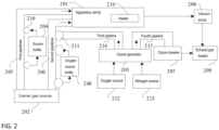
- the apparatus comprises: a carrier gas source 202, a plurality of first pipelines 205, a plurality of second pipelines 206, a source bottle 204, an ozone generator 203, a plurality of first fluid valves 210, a plurality of second fluid valves 211, and an apparatus cavity 201.
- the apparatus cavity 201 is applied to accommodating a substrate and serving as a reaction place thereof. Both the first pipelines 205 and the second pipelines 206 are applied to transmitting carrier gas to the apparatus cavity 201.
- the carrier gas source 202 may further be applied to supplying a non-reactive gas.
- the first fluid valves 210 and the second fluid valves 211 are arranged as a solenoid valve or any other kind of valves.
- the apparatus cavity 201 may be any three-dimensional structure prepared by a plurality of other materials.
- the apparatus cavity 201 may have more than two gas inlets arranged.
- the source bottle 204 may be arranged at any position on the first pipelines 205.
- the carrier gas source 202 may have a conversion valve arranged, the conversion valve is applied to supplying the carrier gas to the first pipelines 205 or the second pipelines 206 selectively in a same flow.
- the conversion valve may directly change the carrier gas introduced into the first pipelines 205 to be introduced into the second pipelines 206 with a same flow, may also increase a flow of gas introduced into the second pipelines 206 at a same time of reducing that being introduced into the first pipelines 205 gradually, while the flow reduced in the first pipelines is as same as that increased in the second pipelines, making total flows of gas entering the cavity through the first pipelines 205 and through the second pipelines 206 are a same.
- the ozone generator 203 has the third pipeline 214 connected, the third pipeline 214 is communicated with the second pipelines 206, and the third pipeline 214 has a flow meter (not shown in the figures) arranged inside, while the flow meter detects a flow of gas in the third pipeline.
- the second pipelines 206 have an exhaust pipeline arranged at a place close to the carrier gas source 202.
- An exhaust pipeline is arranged on the second pipelines 206 at a place close to the carrier gas source 202.
- the exhaust pipeline comprises a flow controller, and the flow controller controls a flow in the exhaust pipeline to be as same as that of gas detected by the flow meter.
- a flow of gas in the third pipeline is as same as that of exhausted gas, a flow of gas flowing into the cavity will not be changed.
- the first pipelines 205 When adopting the source bottle 204 as an oxygen source to the second pipelines 206, if the flow difference before and after introducing the carrier gas into the source bottle 204 is over large, it is possible to adopt the gas exhaust pipeline of the second pipelines 206 to achieve an adjustment and control of the flow difference, before finally keeping the flow of the gas entering the cavity constant.
- the conversion valve is applied to selecting to supply the carrier gas in a same flow to the first pipelines 205 or the second pipelines 206, such that when carrying out an ALD reaction, a flow of the gas being introduced in a purging process between two half reactions is same, that lowers any variations of gas pressure and flow field between different processes, thereby keeping a constant gas pressure and gas flow during a whole ALD process, thus balancing a reaction process, and ensuring film forming quality and stable performance of a final cell.
- the anti-oxidation treatment comprises coating of silicon oxide.
- the anti-oxidation treatment may comprise coating of any other anti-oxidation materials.
- the apparatus further comprises a vacuum pump 208.
- the vacuum pump 208 is applied to pumping out gas from the apparatus cavity 201.
- the vacuum pump 208 may be arranged as a suction pump or other negative pressure equipment.
- the apparatus further comprises an exhaust gas treater 209.
- the exhaust gas treater 209 is applied to processing gas pumped out from the apparatus cavity 201.
- the exhaust gas treater 209 is also applied to processing gas exhausted from the ozone destructor 207.
- the apparatus cavity 201 has a heater 216 arranged, and the heater 216 is applied to controlling a reaction temperature of the apparatus cavity 201.
- the apparatus cavity 201 further has an auxiliary heat tube (not shown in the figure) arranged, the auxiliary heat tube (not shown in the figures) is applied to heating, such that the apparatus cavity 201 can be rapidly heated up to satisfy a requirement of a silicon nitride process.
- the auxiliary heat tube is arranged at an inner top of a furnace tube. After the aluminum oxide process is completed in the apparatus cavity 201, the auxiliary heat tube (not shown in the figures) is open to enable a faster temperature rise of the apparatus cavity 201, so as to shorten a temperature rise period as much as possible, and improve processing efficiency.
- the heater 216 may be arranged in any forms, as long as it is possible to achieve an effect of enabling the substrate to reach a desired heating temperature and keeping a continuous temperature control.
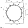
- the apparatus cavity 201 has a plurality of graphite boats arranged inside.
- a number of the graphite boats is N, and N is a positive integer.
- the graphite boat is applied to loading the substrates.
- a number of the substrates loaded by the graphite boat is M, and M is a positive integer.
- the first processing unit is a thermal ALD processing unit, and at least one path of gas in the thermal ALD processing unit is introduced into the apparatus cavity in a pulse mode; and the second processing unit is a PECVD processing unit, and gas in the PECVD processing unit is introduced into a same apparatus cavity in a non-pulse mode.
- the PECVD processing unit and the thermal ALD processing unit share the carrier gas source, the source bottle, and the apparatus cavity.
- the first processing unit is a thermal atomic layer deposition processing unit (that is, a thermal ALD processing unit), and at least one path of gas in the thermal ALD processing unit is introduced into the apparatus cavity in a pulse mode, so as to form a first deposition layer on the substrate.
- the second processing unit is a plasma enhanced chemical vapor deposition unit (that is, a PECVD processing unit), gas of the PECVD processing unit is introduced into a same apparatus cavity in a non-pulse mode, so as to further form a second deposition layer different from the first deposition layer on the substrate.
- the carrier gas source has the conversion valve arranged, and the conversion valve is applied to selecting to supply the carrier gas in a same flow to the first pipelines or the second pipelines, that is, the carrier gas source introduces continuously a same flow of the carrier gas into a same tubular cavity alternately through the first pipelines and the second pipelines by the conversion valve.
- a heating period for the heater 216 to heat up the substrate is 5 to 10 minutes, the heating period depending on a state of the graphite boats and a state of the cavity being heated up.
- the pressure maintaining test comprises that the apparatus cavity 201 has a pressure change no more than 3Pa in 15s.
- the gas pumped out from the apparatus cavity 201 by the vacuum pump 208 is introduced into the exhaust gas treater 209.
- the gas exhausted from the ozone destructor 207 is introduced into the exhaust gas treater 209.
- the substrate continues to subject the PECVD process in the apparatus cavity 201.
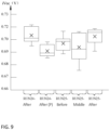
- a plurality of parameters adopted by the substrate treating method are shown as Table 1, and the temperatures of the apparatus cavity 201 at moments T1-T6 are all set as 200 degrees Celsius.
- the carrier gas source 202 adopts argon with a flow value of 2500 standard milliliters per minute.
- a flow value of the ozone is set as 3000 standard milliliters per minute and a concentration as 18.5 wt%.
- the chemical source adopts trimethylaluminum (TMA).
- TMA trimethylaluminum
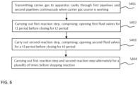
- the first fluid valves 210 are open for 5 seconds before being closed for 7 seconds.
- the second fluid valves 211 are open for 7 seconds before being closed for 8 seconds.
- An operation of 27 seconds in total stated above is one cycle.
- the graphite boats are arranged as eight: A-H.
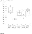
- Each graphite boat has 56 substrates loaded, and each substrate has a unique location in the graphite boat. After the cycle has been carried out for 500 times, a thickness test is carried out onto a substrate testing point by an elliptical polarizer.
- the substrate continues to subject the PECVD process in the same tubular cavity.
- the first deposition layer in the tubular cavity in a pulse mode based on the thermal ALD processing, including aluminum oxide, silicon oxide, gallium oxide, titanium oxide or other oxides; followed by forming the second deposition layer different from the first deposition layer in the same tubular cavity in a non-pulse mode by the PECVD processing, such as silicon nitride.
- the first deposition lay and the second deposition layer are formed in the same tubular cavity, and the second deposition layer is formed by the PECVD unit in the non-pulse mode in the tubular cavity, while the first deposition layer is formed by the thermal ALD processing unit in a pulse mode in the same tubular cavity, thus the first deposition layer often cannot be deposited on the substrate uniformly, which affects the molding quality of a chip substrate seriously, and often causes an unqualified product.
- the heater heats up the substrate; the carrier gas source fills the carrier gas into the tubular cavity before carrying out a pressure maintaining test, while the vacuum pump pumps out gas in the tubular cavity.
- the carrier gas source introduces continuously a same flow of carrier gas into the same tubular cavity alternately through the first pipelines and the second pipelines by the conversion valve.
- the ozone generator is communicated to the third pipeline and kept in an on state, the ozone generator introduces the ozone of a first flow into the second pipelines through the third pipeline.
- the third pipeline has a flow meter arranged in, and the flow meter is applied to detecting a flow of the ozone in the third pipeline; meanwhile, the second pipelines has an exhaust pipeline arranged at a place close to the carrier gas source, a flow controller on the exhaust pipeline is applied to controlling the exhaust pipeline to exhaust gas from the second pipelines, making a flow of the exhausted gas from the second pipelines as same as that of the ozone detected by the flow meter in the third pipeline, so as to ensure a sum of the flow of the carrier gas obtained from the second pipelines and a flow of the ozone obtained from the second pipelines through the third pipeline to be as same as the flow of the carrier gas obtained from the first pipelines.
- FIG. 7 illustrates a schematic diagram on a region division to the substrate according to the present application.
- the substrate is divided into X regions, and X is a positive integer.
- a diameter of the substrate is any size smaller than a size of the graphite boat.
Landscapes
- Chemical & Material Sciences (AREA)
- Engineering & Computer Science (AREA)
- Materials Engineering (AREA)
- General Chemical & Material Sciences (AREA)
- Chemical Kinetics & Catalysis (AREA)
- Mechanical Engineering (AREA)
- Metallurgy (AREA)
- Organic Chemistry (AREA)
- Inorganic Chemistry (AREA)
- Plasma & Fusion (AREA)
- Physics & Mathematics (AREA)
- Analytical Chemistry (AREA)
- Chemical Vapour Deposition (AREA)
- Formation Of Insulating Films (AREA)
Applications Claiming Priority (2)
| Application Number | Priority Date | Filing Date | Title |
|---|---|---|---|
| CN202210547272.8A CN114959649A (zh) | 2022-05-19 | 2022-05-19 | 一种基片处理设备和方法 |
| PCT/CN2023/094772 WO2023222033A1 (fr) | 2022-05-19 | 2023-05-17 | Appareil et procédé de traitement de substrat |
Publications (4)
| Publication Number | Publication Date |
|---|---|
| EP4394079A1 true EP4394079A1 (fr) | 2024-07-03 |
| EP4394079A4 EP4394079A4 (fr) | 2025-04-30 |
| EP4394079B1 EP4394079B1 (fr) | 2026-02-04 |
| EP4394079C0 EP4394079C0 (fr) | 2026-02-04 |
Family
ID=82986007
Family Applications (1)
| Application Number | Title | Priority Date | Filing Date |
|---|---|---|---|
| EP23806984.3A Active EP4394079B1 (fr) | 2022-05-19 | 2023-05-17 | Appareil et procédé de traitement de substrat |
Country Status (5)
| Country | Link |
|---|---|
| US (1) | US20240392438A1 (fr) |
| EP (1) | EP4394079B1 (fr) |
| CN (1) | CN114959649A (fr) |
| ES (1) | ES3062096T3 (fr) |
| WO (1) | WO2023222033A1 (fr) |
Families Citing this family (1)
| Publication number | Priority date | Publication date | Assignee | Title |
|---|---|---|---|---|
| CN114959649A (zh) * | 2022-05-19 | 2022-08-30 | 江苏微导纳米科技股份有限公司 | 一种基片处理设备和方法 |
Family Cites Families (17)
| Publication number | Priority date | Publication date | Assignee | Title |
|---|---|---|---|---|
| US7393561B2 (en) * | 1997-08-11 | 2008-07-01 | Applied Materials, Inc. | Method and apparatus for layer by layer deposition of thin films |
| JP3864585B2 (ja) * | 1998-11-04 | 2007-01-10 | 住友金属工業株式会社 | ステンレス鋼管内面の酸化処理方法 |
| KR100496906B1 (ko) * | 2002-10-21 | 2005-06-28 | 주식회사 아이피에스 | Ald 박막증착장치 |
| JP2009076881A (ja) * | 2007-08-30 | 2009-04-09 | Tokyo Electron Ltd | 処理ガス供給システム及び処理装置 |
| US8728239B2 (en) * | 2011-07-29 | 2014-05-20 | Asm America, Inc. | Methods and apparatus for a gas panel with constant gas flow |
| JP6346022B2 (ja) * | 2013-07-31 | 2018-06-20 | 京セラ株式会社 | 薄膜形成方法および太陽電池素子の製造方法 |
| CN107119264B (zh) * | 2017-06-14 | 2019-03-08 | 东南大学 | 同腔原位复合沉积铱-氧化铝高温涂层设备与工艺 |
| CN109423695B (zh) * | 2017-08-31 | 2021-06-04 | 中国科学院苏州纳米技术与纳米仿生研究所 | 掺杂源供应管路及化学气相沉积系统 |
| CN107868944B (zh) * | 2017-10-31 | 2020-02-07 | 北京北方华创微电子装备有限公司 | 一种氮化钛原子层沉积装置及其沉积方法 |
| CN207933525U (zh) * | 2018-02-06 | 2018-10-02 | 江苏微导纳米装备科技有限公司 | 一种真空反应装置及反应腔 |
| CN108149225A (zh) * | 2018-02-06 | 2018-06-12 | 江苏微导纳米装备科技有限公司 | 一种真空反应装置及反应方法 |
| CN109518164A (zh) * | 2018-12-20 | 2019-03-26 | 北京北方华创微电子装备有限公司 | 原子层沉积设备及方法 |
| CN111304633B (zh) * | 2020-03-23 | 2022-07-22 | 北京北方华创微电子装备有限公司 | 气相沉积设备以及气相沉积方法 |
| CN111560605A (zh) * | 2020-06-18 | 2020-08-21 | 北京北方华创微电子装备有限公司 | 原子层沉积设备的前驱体传输装置和前驱体传输方法 |
| CN213146096U (zh) * | 2020-08-06 | 2021-05-07 | 北京北方华创微电子装备有限公司 | 半导体工艺设备的进气装置及半导体工艺设备 |
| CN113416945B (zh) * | 2021-06-24 | 2022-10-21 | 北京北方华创微电子装备有限公司 | 原子层沉积设备的进气装置及原子层沉积设备 |
| CN114959649A (zh) * | 2022-05-19 | 2022-08-30 | 江苏微导纳米科技股份有限公司 | 一种基片处理设备和方法 |
-
2022
- 2022-05-19 CN CN202210547272.8A patent/CN114959649A/zh active Pending
-
2023
- 2023-05-17 WO PCT/CN2023/094772 patent/WO2023222033A1/fr not_active Ceased
- 2023-05-17 EP EP23806984.3A patent/EP4394079B1/fr active Active
- 2023-05-17 ES ES23806984T patent/ES3062096T3/es active Active
- 2023-05-17 US US18/695,828 patent/US20240392438A1/en active Pending
Also Published As
| Publication number | Publication date |
|---|---|
| EP4394079A4 (fr) | 2025-04-30 |
| EP4394079B1 (fr) | 2026-02-04 |
| ES3062096T3 (en) | 2026-04-08 |
| US20240392438A1 (en) | 2024-11-28 |
| WO2023222033A1 (fr) | 2023-11-23 |
| EP4394079C0 (fr) | 2026-02-04 |
| CN114959649A (zh) | 2022-08-30 |
Similar Documents
| Publication | Publication Date | Title |
|---|---|---|
| KR100257302B1 (ko) | 성막방법 | |
| US7482283B2 (en) | Thin film forming method and thin film forming device | |
| US8685866B2 (en) | Method of manufacturing semiconductor device and substrate processing apparatus | |
| CN100392148C (zh) | 用单晶片低压cvd淀积氧化硅和氮氧化物的方法 | |
| US8202809B2 (en) | Method of manufacturing semiconductor device, method of processing substrate, and substrate processing apparatus | |
| US9624579B2 (en) | Film forming apparatus, film forming method, and non-transitory computer-readable storage medium | |
| US10428426B2 (en) | Method and apparatus to prevent deposition rate/thickness drift, reduce particle defects and increase remote plasma system lifetime | |
| US20150140839A1 (en) | Substrate processing apparatus | |
| US20140023794A1 (en) | Method And Apparatus For Low Temperature ALD Deposition | |
| JP2014067783A (ja) | 基板処理装置、半導体装置の製造方法及び基板処理方法 | |
| US12014920B2 (en) | Apparatus for hydrogen assisted atmospheric radical oxidation | |
| US20160064190A1 (en) | Substrate processing apparatus | |
| US20170117145A1 (en) | Boron nitride film forming method and semiconductor device manufacturing method | |
| EP3751018A1 (fr) | Dispositif de réaction sous vide et procédé de réaction | |
| US20050136693A1 (en) | Thermal processing unit and thermal processing method | |
| EP4394079B1 (fr) | Appareil et procédé de traitement de substrat | |
| TW201903848A (zh) | 用來在半導體基材上形成膜層的方法與裝置及半導體基材 | |
| US20140242810A1 (en) | Substrate processing apparatus and method of supplying and exhausting gas | |
| JP2013151722A (ja) | 半導体装置の製造方法 | |
| CN117144339A (zh) | 薄膜沉积方法及设备 | |
| JP3960987B2 (ja) | 反応容器 | |
| US20250279289A1 (en) | Vaporization system and semiconductor process equipment | |
| TWI720412B (zh) | 半導體裝置之製造方法、基板處理裝置及記錄媒體 | |
| JP2011142347A (ja) | 基板処理装置 | |
| CN223561687U (zh) | 原子层沉积设备的进气装置及原子层沉积设备 |
Legal Events
| Date | Code | Title | Description |
|---|---|---|---|
| STAA | Information on the status of an ep patent application or granted ep patent |
Free format text: STATUS: THE INTERNATIONAL PUBLICATION HAS BEEN MADE |
|
| PUAI | Public reference made under article 153(3) epc to a published international application that has entered the european phase |
Free format text: ORIGINAL CODE: 0009012 |
|
| STAA | Information on the status of an ep patent application or granted ep patent |
Free format text: STATUS: REQUEST FOR EXAMINATION WAS MADE |
|
| 17P | Request for examination filed |
Effective date: 20240327 |
|
| AK | Designated contracting states |
Kind code of ref document: A1 Designated state(s): AL AT BE BG CH CY CZ DE DK EE ES FI FR GB GR HR HU IE IS IT LI LT LU LV MC ME MK MT NL NO PL PT RO RS SE SI SK SM TR |
|
| RIN1 | Information on inventor provided before grant (corrected) |
Inventor name: WANG, YUNSONG Inventor name: ZHANG, PENG Inventor name: LI, WEI MIN Inventor name: LI, XIANG Inventor name: LIAO, BAOCHEN Inventor name: WU, XINYUAN |
|
| A4 | Supplementary search report drawn up and despatched |
Effective date: 20250328 |
|
| RIC1 | Information provided on ipc code assigned before grant |
Ipc: H10F 71/00 20250101ALI20250324BHEP Ipc: H01L 21/67 20060101ALI20250324BHEP Ipc: H01L 21/02 20060101ALI20250324BHEP Ipc: H01J 37/32 20060101ALI20250324BHEP Ipc: C23C 16/54 20060101ALI20250324BHEP Ipc: C23C 16/44 20060101ALI20250324BHEP Ipc: H01L 21/316 20060101ALI20250324BHEP Ipc: C23C 16/52 20060101ALI20250324BHEP Ipc: C23C 16/34 20060101ALI20250324BHEP Ipc: C23C 16/40 20060101ALI20250324BHEP Ipc: C23C 16/50 20060101ALI20250324BHEP Ipc: C23C 16/455 20060101AFI20250324BHEP |
|
| DAV | Request for validation of the european patent (deleted) | ||
| DAX | Request for extension of the european patent (deleted) | ||
| GRAP | Despatch of communication of intention to grant a patent |
Free format text: ORIGINAL CODE: EPIDOSNIGR1 |
|
| STAA | Information on the status of an ep patent application or granted ep patent |
Free format text: STATUS: GRANT OF PATENT IS INTENDED |
|
| INTG | Intention to grant announced |
Effective date: 20250924 |
|
| GRAS | Grant fee paid |
Free format text: ORIGINAL CODE: EPIDOSNIGR3 |
|
| GRAA | (expected) grant |
Free format text: ORIGINAL CODE: 0009210 |
|
| STAA | Information on the status of an ep patent application or granted ep patent |
Free format text: STATUS: THE PATENT HAS BEEN GRANTED |
|
| AK | Designated contracting states |
Kind code of ref document: B1 Designated state(s): AL AT BE BG CH CY CZ DE DK EE ES FI FR GB GR HR HU IE IS IT LI LT LU LV MC ME MK MT NL NO PL PT RO RS SE SI SK SM TR |
|
| REG | Reference to a national code |
Ref country code: CH Ref legal event code: F10 Free format text: ST27 STATUS EVENT CODE: U-0-0-F10-F00 (AS PROVIDED BY THE NATIONAL OFFICE) Effective date: 20260204 Ref country code: GB Ref legal event code: FG4D |
|
| REG | Reference to a national code |
Ref country code: IE Ref legal event code: FG4D |
|
| U01 | Request for unitary effect filed |
Effective date: 20260204 |
|
| U07 | Unitary effect registered |
Designated state(s): AT BE BG DE DK EE FI FR IT LT LU LV MT NL PT RO SE SI Effective date: 20260209 |
|
| REG | Reference to a national code |
Ref country code: ES Ref legal event code: FG2A Ref document number: 3062096 Country of ref document: ES Kind code of ref document: T3 Effective date: 20260408 |
|
| U20 | Renewal fee for the european patent with unitary effect paid |
Year of fee payment: 4 Effective date: 20260407 |