EP4394094A1 - Cristal de nitrure de gallium, substrat de nitrure de gallium et procédé de production de cristal de nitrure de gallium - Google Patents
Cristal de nitrure de gallium, substrat de nitrure de gallium et procédé de production de cristal de nitrure de gallium Download PDFInfo
- Publication number
- EP4394094A1 EP4394094A1 EP22861365.9A EP22861365A EP4394094A1 EP 4394094 A1 EP4394094 A1 EP 4394094A1 EP 22861365 A EP22861365 A EP 22861365A EP 4394094 A1 EP4394094 A1 EP 4394094A1
- Authority
- EP
- European Patent Office
- Prior art keywords
- main surface
- crystal
- less
- line segment
- gallium nitride
- Prior art date
- Legal status (The legal status is an assumption and is not a legal conclusion. Google has not performed a legal analysis and makes no representation as to the accuracy of the status listed.)
- Pending
Links
Images
Classifications
-
- C—CHEMISTRY; METALLURGY
- C30—CRYSTAL GROWTH
- C30B—SINGLE-CRYSTAL GROWTH; UNIDIRECTIONAL SOLIDIFICATION OF EUTECTIC MATERIAL OR UNIDIRECTIONAL DEMIXING OF EUTECTOID MATERIAL; REFINING BY ZONE-MELTING OF MATERIAL; PRODUCTION OF A HOMOGENEOUS POLYCRYSTALLINE MATERIAL WITH DEFINED STRUCTURE; SINGLE CRYSTALS OR HOMOGENEOUS POLYCRYSTALLINE MATERIAL WITH DEFINED STRUCTURE; AFTER-TREATMENT OF SINGLE CRYSTALS OR A HOMOGENEOUS POLYCRYSTALLINE MATERIAL WITH DEFINED STRUCTURE; APPARATUS THEREFOR
- C30B7/00—Single-crystal growth from solutions using solvents which are liquid at normal temperature, e.g. aqueous solutions
- C30B7/10—Single-crystal growth from solutions using solvents which are liquid at normal temperature, e.g. aqueous solutions by application of pressure, e.g. hydrothermal processes
- C30B7/105—Single-crystal growth from solutions using solvents which are liquid at normal temperature, e.g. aqueous solutions by application of pressure, e.g. hydrothermal processes using ammonia as solvent, i.e. ammonothermal processes
-
- C—CHEMISTRY; METALLURGY
- C30—CRYSTAL GROWTH
- C30B—SINGLE-CRYSTAL GROWTH; UNIDIRECTIONAL SOLIDIFICATION OF EUTECTIC MATERIAL OR UNIDIRECTIONAL DEMIXING OF EUTECTOID MATERIAL; REFINING BY ZONE-MELTING OF MATERIAL; PRODUCTION OF A HOMOGENEOUS POLYCRYSTALLINE MATERIAL WITH DEFINED STRUCTURE; SINGLE CRYSTALS OR HOMOGENEOUS POLYCRYSTALLINE MATERIAL WITH DEFINED STRUCTURE; AFTER-TREATMENT OF SINGLE CRYSTALS OR A HOMOGENEOUS POLYCRYSTALLINE MATERIAL WITH DEFINED STRUCTURE; APPARATUS THEREFOR
- C30B29/00—Single crystals or homogeneous polycrystalline material with defined structure characterised by the material or by their shape
- C30B29/10—Inorganic compounds or compositions
- C30B29/40—AIIIBV compounds wherein A is B, Al, Ga, In or Tl and B is N, P, As, Sb or Bi
- C30B29/403—AIII-nitrides
- C30B29/406—Gallium nitride
Definitions
- these devices be produced using a high-quality semiconductor substrate (free-standing substrate) made of the same kind of material and having few crystal defects, and a technique of producing a GaN crystal that can be used for such semiconductor substrates has been actively studied.
- the HVPE method is a method in which a chloride of Ga and NH 3 are introduced into a furnace in a hydrogen stream and thermally decomposed to deposit crystals generated by thermal decomposition on a substrate.
- a (0001) crystal plane and a (000-1) crystal plane are collectively referred to as a c-plane, a ⁇ 10-10 ⁇ crystal plane is referred to as an m-plane, and a ⁇ 11-20 ⁇ crystal plane is referred to as an a-plane.
- a crystal axis perpendicular to the c-plane is called a c-axis
- a crystal axis perpendicular to the m-plane is called an m-axis
- a crystal axis perpendicular to the a-plane is called an a-axis.
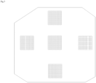
- a first line segment which is a virtual line segment extending in a first direction on the specific main surface A and having a length of 40 mm and a second line segment which is a virtual line segment extending in a second direction perpendicular to the first direction on the specific main surface A and having a length of 40 mm can be drawn, and a facet growth region density in a random square region of 1 cm ⁇ 1 cm on the specific main surface A does not exceed 100 cm -2 .
- a first line segment which is a virtual line segment extending in a first direction on the specific main surface A and having a length of 40 mm and a second line segment which is a virtual line segment extending in a second direction perpendicular to the first direction on the specific main surface A and having a length of 40 mm can be drawn, and a ratio of an area of facet growth regions to an area of the specific main surface A (area of facet growth regions/area of specific main surface A) is 10% or less.
- the GaN crystal of the third aspect preferably includes the main surface 2, having an inclination of 0 degrees or more and 10 degrees or less from a (0001) crystal plane which is a main surface on an opposite side of the main surface 1.
- a method for observing the number of facet growth regions is not particularly limited as long as the facet growth regions can be specified, and for example, a method for observing the number of pits derived from the facet growth regions visually or with a microscope or the like, a method for observing bright regions of a yellow band in a photoluminescence (PL) image, or the like can be used.
- a method for observing the number of pits derived from the facet growth regions visually or with a microscope or the like a method for observing bright regions of a yellow band in a photoluminescence (PL) image, or the like can be used.
- PL photoluminescence
- a diameter of a main surface of the GaN crystal is not particularly limited, and is preferably 45 mm or more, and can be 50 mm or more, 60 mm or more, 80 mm or more, or 100 mm or more in stages. Typically, the diameter is 45 to 55 mm (about 2 inches), 95 to 105 mm (about 4 inches), 145 to 155 mm (about 6 inches), 195 to 205 mm (about 8 inches), 295 to 305 mm (about 12 inches), and the like.
- a surface area of the main surface of the GaN crystal is not particularly limited, and is preferably 15 cm 2 or more, and may be 15 cm 2 or more and less than 50 cm 2 , 50 cm 2 or more and less than 100 cm 2 , 100 cm 2 or more and less than 200 cm 2 , 200 cm 2 or more and less than 350 cm 2 , 350 cm 2 or more and less than 500 cm 2 , 500 cm 2 or more and less than 750 cm 2 , or the like.
- a maximum area, that can be taken, of a cross-section perpendicular to the growth direction of the crystal satisfy these numerical ranges.
- the concentration of hydrogen (H) in the GaN crystal is preferably 2 ⁇ 10 19 atoms/cm 3 or less, more preferably 1 ⁇ 10 19 atoms/cm 3 or less, still more preferably 5 ⁇ 10 18 atoms/cm 3 or less, and particularly preferably 1 ⁇ 10 18 atoms/cm 3 or less.
- hydrogen (H) is contained at a concentration of 1 ⁇ 10 17 atoms/cm 3 or more.
- the concentration of oxygen (O) in the GaN crystal is preferably 2 ⁇ 10 19 atoms/cm 3 or less, more preferably 1 ⁇ 10 19 atoms/cm 3 or less, still more preferably 5 ⁇ 10 18 atoms/cm 3 or less, and particularly preferably 1 ⁇ 10 18 atoms/cm 3 or less.
- H hydrogen
- O oxygen
- halogen element other than fluorine examples include chlorine (Cl), bromine (Br), and iodine (I), and it is preferable that the halogen element substantially contained in the GaN crystal is only fluorine.
- Such crystals are obtained, for example, by using only a mineralizer containing F as a halogen.
- An example of a preferred aspect of the GaN crystal of the present embodiment is as follows.
- a gallium nitride crystal which contains a halogen element in the crystal and in which the halogen element substantially contained is only fluorine, the gallium nitride crystal including a main surface 1 having an inclination of 0 degrees or more and 10 degrees or less from a (000-1) crystal plane, in which the main surface 1 is a specific main surface A satisfying at least one of the following conditions (A1) to (A3).
- a first line segment which is a virtual line segment extending in a first direction on the specific main surface A and having a length of 40 mm and a second line segment which is a virtual line segment extending in a second direction perpendicular to the first direction on the specific main surface A and having a length of 40 mm can be drawn, and a facet growth region density in a random square region of 10 mm ⁇ 10 mm on the specific main surface A does not exceed 500 cm -2 , and preferably does not exceed 100 cm -2 .
- a first line segment which is a virtual line segment extending in a first direction on the specific main surface A and having a length of 40 mm and a second line segment which is a virtual line segment extending in a second direction perpendicular to the first direction on the specific main surface A and having a length of 40 mm can be drawn, and at least one square region of 20 mm ⁇ 20 mm having a facet growth region density of less than 5 cm -2 is found in the specific main surface A.
- the fact that the halogen element substantially contained in the GaN crystal is only fluorine means that the total content of halogen elements other than F in the crystal is 1/100 or less of the content of F.
- a member (for example, a lining material) used for a reaction vessel is hardly corroded.
- the total content of halogen elements other than F in the crystal is more preferably 1/150 or less, and still more preferably 1/200 or less of the content of F.
- a gallium nitride crystal which contains F in the crystal and in which a total content of halogen elements other than F is 1/100 or less of a content of F, the gallium nitride crystal including a main surface 1 having an inclination of 0 degrees or more and 10 degrees or less from a (000-1) crystal plane, in which the main surface 1 is a specific main surface A satisfying at least one of the following conditions (A1) to (A3).
- Specific examples of the surface (growth surface) of the GaN seed for crystal growth on the GaN seed described above include a nitrogen polar surface of the GaN seed.
- a thickness thereof is preferably 300 ⁇ m or more, and if the diameter is larger than this, a preferable lower limit value of the thickness becomes also larger.
- the thickness of the GaN seed is not particularly limited, but is usually 20 mm or less.
- Examples of a preferred embodiment include a step of growing a GaN crystal on a surface of the GaN seed, in a reaction vessel containing a GaN seed having a nitrogen polar surface obtained by a liquid phase growth method, a nitrogen-containing solvent, a raw material, and a mineralizer, by controlling the nitrogen-containing solvent to be in a supercritical state and/or a subcritical state.
- the present inventors have found that a GaN crystal in which generation of specific crystal defects is curbed can be obtained by using the GaN seed described above and satisfying the crystal growth conditions.
- the detailed reason for this is not clear yet, but is presumed as follows. It is considered that, in the formation of the facet growth region on the nitrogen polar surface of the GaN crystal, since a crystal growth rate in the facet plane direction is relatively slow as compared with a crystal growth rate in a (000-1) plane direction, the facet growth region continues to exist without being completely filled. Specifically, it is considered that the growth rate of a facet plane represented by a (10-1-1) plane or a (10-1-2) plane is slower than the growth rate of a (000-1) plane.
- the present inventors have found that the growth rate in a specific facet plane direction can be improved by setting the pressure in the reaction vessel to 200 MPa or less and setting the temperature of the crystal growth region to 600°C or higher, which is a higher temperature as compared with the conventional method. As a result, it is considered that the relative difference in crystal growth rate between the (000-1) plane direction and the facet plane direction decreases, and the formation of the facet growth region can be curbed. It is presumed that the facet growth region density can be greatly improved by a synergistic effect obtained by combining with the suppression effect obtained by adopting the GaN seed obtained by the liquid phase growth method described above. In addition, as will be described later, it is also possible to effectively reduce the facet growth region density by reducing foreign matter externally adhering to the growth surface of the GaN seed.
- the present inventors have found that a GaN crystal in which an area ratio between the main surface 1 and the main surface 2 (main surface 1/main surface 2) is large can be obtained by using the GaN seed described above and satisfying the crystal growth conditions.
- the detailed reason for this is not clear yet, but is presumed as follows.
- a growth rate of a facet plane for example, a (10-1-2) surface
- a growth rate of a facet plane for example, a (10-1-1) surface
- an area of the facet plane having the gentler inclination is enlarged, and accordingly, an area of the main surface (main surface 1) on the nitrogen polar surface side is reduced.
- the mineralizer exhibit negative solubility characteristics in the nitrogen-containing solvent in the vicinity of the temperature at which the GaN crystal is grown.
- ammonium fluoride exhibits negative solubility characteristics in ammonia in a temperature range of 400°C or higher.
- the temperature of the crystal growth region is 450°C or higher, in a case where only ammonium fluoride is used as the mineralizer, ammonium fluoride exhibits negative solubility characteristics at the crystal growth temperature.
- the slope of the solubility curve determined based on each solubility characteristic varies depending on a mixing ratio. When an absolute value of the slope of the solubility curve is small, the efficiency of crystal growth is deteriorated, and thus the mixing ratio is adjusted so that a solubility curve with an appropriate slope is shown.
- the molar concentration of fluorine contained in the mineralizer with respect to the nitrogen-containing solvent is preferably 0.2 mol% or more, more preferably 0.27 mol% or more, still more preferably 1.0 mol% or more, and particularly preferably 1.5 mol% or more, and is preferably 30 mol% or less, more preferably 20 mol% or less, still more preferably 10 mol% or less, and particularly preferably 2 mol% or less.
- concentration is high, the solubility of the raw material in the nitrogen-containing solvent is improved, and the growth rate tends to increase, which is preferable.
- the concentration is low, since the solubility can be appropriately maintained, spontaneous nucleation can be curbed, and the degree of supersaturation can be kept small, so that control is facilitated, which is preferable.
- the crystal is grown by setting the pressure in the reaction vessel during crystal growth to 200 MPa or less.
- the pressure in the reaction vessel is preferably 5 MPa or more, more preferably 10 MPa or more, still more preferably 12 MPa or more, particularly preferably 15 MPa or more, and most preferably 20 MPa or more, and is preferably 150 MPa or less, more preferably 120 MPa or less, and still more preferably 100 MPa or less.
- the production method of the present embodiment is characterized in that a GaN crystal can be efficiently grown even under a relatively low pressure. When the crystal is grown at a relatively low pressure, a thickness of the pressure-resistant container can be reduced, and the energy efficiency can also be increased, thereby curbing the costs.
- the amount of water or oxygen contained in the polycrystalline raw material used as a raw material be small.
- the oxygen content in the polycrystalline raw material is usually 10000 ppm or less, preferably 1000 ppm or less, and particularly preferably 1 ppm or less.
- the ease of incorporating oxygen into the polycrystalline raw material is related to reactivity with moisture or absorption capacity. As the crystallinity of the polycrystalline raw material is worse, more active groups such as NH groups are present on the surface, and there is a possibility that the active groups react with water to partially form oxides and hydroxides. Therefore, it is usually preferable to use a polycrystalline raw material having as high crystallinity as possible.
- the growth reaction of the GaN crystal is performed in a reaction vessel.
- the reaction vessel means a container which is used for producing a GaN crystal in a state in which a nitrogen-containing solvent in a supercritical state and/or a subcritical state can be in direct contact with an inner wall surface thereof, and preferred examples thereof include a structure itself inside the pressure-resistant container and a capsule installed in the pressure-resistant container.
- a pressure-resistant portion of the reaction vessel is preferably made of any one of a Ni-based alloy, an Fe-based alloy, and a cobalt-based alloy, or an alloy obtained by combining these alloys, and is particularly preferably made of a Ni-Fe-based alloy (it is particularly preferable that the Ni-Fe-based alloy have an Fe content of 30 to 40 mass%, and contain Cr, Ti, Al, and Nb as other elements).
- a mode in which the reaction vessel is made using these alloys is not particularly limited.
- the inner surface of the pressure-resistant portion may be directly lined or coated with a material excellent in corrosion resistance to form a reaction vessel, or a capsule made of a material excellent in corrosion resistance may be disposed in the pressure-resistant container.
- a shape of the reaction vessel may be any shape such as a cylindrical shape.
- the reaction vessel may be installed upright, horizontally, or obliquely, and it is particularly preferable to use the reaction vessel in an upright state.
- a platinum group or a platinum group alloy can be used for a lining material or a capsule as the corrosion-resistant portion.
- the platinum group include Pt, Au, Ir, Ru, Rh, Pd, and Ag.
- Ag or an alloy containing Ag can be suitably used as the lining material by using a compound containing fluorine as the mineralizer alone.
- a GaN crystal on a surface of the GaN seed is grown by controlling a solvent to be in a supercritical state and/or a subcritical state.
- the pressure conditions in this case are as described above.
- the temperature at the time of growth is set to temperatures different between the raw material dissolution region in which the raw material dissolves and the crystal growth region in which the crystal is grown on the seed crystal.
- the temperature of the crystal growth region be 600°C or higher.
- the temperature is more preferably 610°C or higher.
- the temperature of the crystal growth region may be higher, and can be preferably set to, for example, 700°C or lower, or 650°C or lower.
- the temperature of the raw material dissolution region is set to be higher than the temperature of the crystal growth region in a case where a mineralizer having negative solubility characteristics is used.
- the temperature is set to be lower than the temperature of the crystal growth region.
- the temperature difference between the raw material dissolution region and the crystal growth region is usually set to 30°C or higher and preferably 40°C or higher, and is usually set to 150°C or lower and preferably 120°C or lower.
- the surface of the GaN seed is also preferable to etch the surface of the GaN seed by adjusting the solubility. As a result, a surface layer portion of the GaN seed dissolves, and a damaged layer that can serve as a starting point of facet growth can be removed.
- a surface (growth surface) of the GaN seed for crystal growth on the GaN seed have fewer growth inhibiting factors that can serve as starting points of facet growth.
- the growth inhibiting factors that can serve as starting points of facet growth include, as described above, crystal defects such as dislocations inherent in GaN seeds, and in addition, foreign matter externally adhering to the surface of the GaN seed can also be the growth inhibiting factors. Examples of such foreign matter include impurities present on an inner wall of the reaction vessel, and fine pieces of GaN polycrystal as a raw material.
- the direction of the growth surface of the GaN seed when the GaN seed is placed in the reaction vessel is parallel to the height direction of the reaction vessel or has a downward angle. In this case, it is possible to prevent foreign matter from externally adhering to the growth surface of the GaN seed, which is desirable from the viewpoint of suppressing facet growth.
- a cleaning method is not particularly limited, and for example, foreign matter adhering to the inner wall can be removed by physical cleaning with a brush or the like or chemical cleaning with an acid, an alkali, or the like.
- a degassing step of heat degassing the inside of the reaction vessel before the growth step described above it is preferable to include a degassing step of heat degassing the inside of the reaction vessel before the growth step described above.
- a method of heat degassing is not particularly limited, and the heat degassing can be performed by a known method, and examples thereof include a method of degassing with a vacuum pump while heating.
- the degree of vacuum at the time of heat degassing is preferably as high as possible, and is usually preferably 5 ⁇ 10 -4 Pa or less, more preferably 1 ⁇ 10 -4 Pa or less, and still more preferably 5 ⁇ 10 -5 Pa or less.
- the heat degassing time is preferably 2 hours or more, more preferably 6 hours or more, further preferably 12 hours or more, preferably 72 hours or less, more preferably 48 hours or less, and particularly preferably 24 hours or less.
- a processing step of processing a GaN crystal may be included after the growth step.
- the processing for example, it is conceivable to acquire only a portion having desired characteristics by slicing the obtained GaN crystal, and it is most preferable to acquire only a portion meeting the range of crystal quality requirements as described above.
- the GaN crystal thus obtained can be used as a GaN substrate to be described later.
- GaN substrate gallium nitride substrate obtained by slicing the GaN crystal, and a method for producing the same.
- a diameter of the GaN substrate is 50 mm or more, typically 50 to 55 mm (about 2 inches), 100 to 105 mm (about 4 inches), 150 to 155 mm (about 6 inches), and the like. Since the GaN substrate is required to have strength enough not to hinder handling, a thickness thereof is usually 250 ⁇ m or more, and can be further increased according to the diameter.
- the thickness is preferably 250 ⁇ m or more and more preferably 300 ⁇ m or more, and is preferably 450 ⁇ m or less and more preferably 400 ⁇ m or less.
- the thickness is preferably 350 ⁇ m or more, more preferably 400 ⁇ m or more, and preferably 750 ⁇ m or less, and more preferably 650 ⁇ m or less.
- XRC X-ray rocking curve
- the ratio of a total areas of the facet growth regions to the area of the main area 1 of the present crystal was 42%.
- a gallium nitride crystal including: a main surface 1 having an inclination of 0 degrees or more and 10 degrees or less from a (000-1) crystal plane; and a main surface 2, having an inclination of 0 degrees or more and 10 degrees or less from a (0001) crystal plane which is a main surface on an opposite side, in which a thickness in a c-axis direction is 1 mm or more, and an area ratio between a (10-1-1) plane and a (10-1-2) plane satisfies the following relational expression (C).
- a method for producing a gallium nitride crystal including: a seed preparation step of preparing a GaN seed which is obtained by a liquid phase growth method and has a nitrogen polar surface; and a crystal growth step of growing a GaN crystal on the nitrogen polar surface of the GaN seed by an ammonothermal method by setting a pressure in a reaction vessel containing a mineralizer containing fluorine to 200 MPa or less and a temperature of a crystal growth region to 600°C or higher.
- a high-quality GaN crystal with curbed specific defects can be produced.
- the GaN crystal efficiently produced by the producing method of the present disclosure can be applied not only to blue light emitting diodes (LED) and blue semiconductor lasers (LD) made of nitride-based semiconductors of Group 13 elements of the periodic table, but also to a wide range of applications such as GaN substrates for power semiconductor elements (power devices) and high frequency power devices. Therefore, the industrial applicability of the present disclosure is extremely high.
Landscapes
- Chemical & Material Sciences (AREA)
- Engineering & Computer Science (AREA)
- Crystallography & Structural Chemistry (AREA)
- Materials Engineering (AREA)
- Metallurgy (AREA)
- Organic Chemistry (AREA)
- Inorganic Chemistry (AREA)
- Crystals, And After-Treatments Of Crystals (AREA)
Applications Claiming Priority (2)
| Application Number | Priority Date | Filing Date | Title |
|---|---|---|---|
| JP2021137526 | 2021-08-25 | ||
| PCT/JP2022/031744 WO2023027077A1 (fr) | 2021-08-25 | 2022-08-23 | Cristal de nitrure de gallium, substrat de nitrure de gallium et procédé de production de cristal de nitrure de gallium |
Publications (2)
| Publication Number | Publication Date |
|---|---|
| EP4394094A1 true EP4394094A1 (fr) | 2024-07-03 |
| EP4394094A4 EP4394094A4 (fr) | 2025-08-20 |
Family
ID=85322855
Family Applications (1)
| Application Number | Title | Priority Date | Filing Date |
|---|---|---|---|
| EP22861365.9A Pending EP4394094A4 (fr) | 2021-08-25 | 2022-08-23 | Cristal de nitrure de gallium, substrat de nitrure de gallium et procédé de production de cristal de nitrure de gallium |
Country Status (7)
| Country | Link |
|---|---|
| US (1) | US20240191395A1 (fr) |
| EP (1) | EP4394094A4 (fr) |
| JP (1) | JPWO2023027077A1 (fr) |
| KR (1) | KR20240051191A (fr) |
| CN (1) | CN117897521A (fr) |
| TW (1) | TW202314971A (fr) |
| WO (1) | WO2023027077A1 (fr) |
Families Citing this family (1)
| Publication number | Priority date | Publication date | Assignee | Title |
|---|---|---|---|---|
| JP7195431B2 (ja) * | 2019-06-27 | 2022-12-23 | 三菱電機株式会社 | 光半導体装置の製造方法 |
Family Cites Families (13)
| Publication number | Priority date | Publication date | Assignee | Title |
|---|---|---|---|---|
| JP4229624B2 (ja) | 2002-03-19 | 2009-02-25 | 三菱化学株式会社 | 窒化物単結晶の製造方法 |
| JP4433696B2 (ja) | 2003-06-17 | 2010-03-17 | 三菱化学株式会社 | 窒化物結晶の製造方法 |
| WO2009149299A1 (fr) * | 2008-06-04 | 2009-12-10 | Sixpoint Materials | Procédés de création des cristaux de nitrure du groupe iii de cristallinité améliorée à partir de germe de nitrure du groupe iii initial par croissance ammoniothermique |
| US9589792B2 (en) * | 2012-11-26 | 2017-03-07 | Soraa, Inc. | High quality group-III metal nitride crystals, methods of making, and methods of use |
| WO2010079814A1 (fr) | 2009-01-08 | 2010-07-15 | 三菱化学株式会社 | Procédé de fabrication de cristal de nitrure, cristal de nitrure et dispositif de fabrication de celui-ci |
| EP2660365B1 (fr) * | 2010-12-27 | 2023-03-22 | Mitsubishi Chemical Corporation | Procédé et dispositif de fabrication de cristal semi-conducteur de gan |
| JP2013038116A (ja) * | 2011-08-04 | 2013-02-21 | Sumitomo Electric Ind Ltd | Iii族窒化物結晶基板の製造方法 |
| JP5733120B2 (ja) * | 2011-09-09 | 2015-06-10 | 住友電気工業株式会社 | ソーワイヤおよびそれを用いたiii族窒化物結晶基板の製造方法 |
| JP6024335B2 (ja) * | 2012-09-21 | 2016-11-16 | 三菱化学株式会社 | 周期表第13属金属窒化物半導体基板の製造方法 |
| WO2014129544A1 (fr) * | 2013-02-22 | 2014-08-28 | 三菱化学株式会社 | Cristal de nitrure de métal du groupe 13 du tableau périodique, et son procédé de production |
| WO2015107813A1 (fr) * | 2014-01-17 | 2015-07-23 | 三菱化学株式会社 | SUBSTRAT GaN, SON PROCÉDÉ DE PRODUCTION, PROCÉDÉ DE PRODUCTION D'UN CRISTAL GaN, ET PROCÉDÉ DE FABRICATION D'UN DISPOSITIF À SEMI-CONDUCTEURS |
| JP2015178438A (ja) * | 2014-02-28 | 2015-10-08 | 三菱化学株式会社 | 窒化ガリウム自立基板、窒化ガリウム結晶及び窒化ガリウム自立基板の生産方法 |
| KR102426231B1 (ko) * | 2016-08-08 | 2022-07-29 | 미쯔비시 케미컬 주식회사 | 도전성 C면 GaN 기판 |
-
2022
- 2022-08-23 EP EP22861365.9A patent/EP4394094A4/fr active Pending
- 2022-08-23 KR KR1020247009295A patent/KR20240051191A/ko active Pending
- 2022-08-23 JP JP2023543934A patent/JPWO2023027077A1/ja active Pending
- 2022-08-23 CN CN202280057716.8A patent/CN117897521A/zh active Pending
- 2022-08-23 WO PCT/JP2022/031744 patent/WO2023027077A1/fr not_active Ceased
- 2022-08-23 TW TW111131668A patent/TW202314971A/zh unknown
-
2024
- 2024-02-23 US US18/585,407 patent/US20240191395A1/en active Pending
Also Published As
| Publication number | Publication date |
|---|---|
| JPWO2023027077A1 (fr) | 2023-03-02 |
| TW202314971A (zh) | 2023-04-01 |
| EP4394094A4 (fr) | 2025-08-20 |
| CN117897521A (zh) | 2024-04-16 |
| US20240191395A1 (en) | 2024-06-13 |
| KR20240051191A (ko) | 2024-04-19 |
| WO2023027077A1 (fr) | 2023-03-02 |
Similar Documents
| Publication | Publication Date | Title |
|---|---|---|
| US12107129B2 (en) | Self-standing GaN substrate, GaN crystal, method for producing GaN single crystal, and method for producing semiconductor device | |
| KR20090064379A (ko) | 질화물 반도체의 제조 방법, 결정 성장 속도 증가제, 질화물 단결정, 웨이퍼 및 디바이스 | |
| US20100111808A1 (en) | Group-iii nitride monocrystal with improved crystal quality grown on an etched-back seed crystal and method of producing the same | |
| JP5888208B2 (ja) | 窒化物結晶の製造方法 | |
| TW202020940A (zh) | n型GaN結晶、GaN晶圓、及GaN結晶、GaN晶圓和氮化物半導體裝置的製造方法 | |
| JP6020440B2 (ja) | 窒化物結晶の製造方法 | |
| US20100075107A1 (en) | Hexagonal wurtzite single crystal and hexagonal wurtzite single crystal substrate | |
| US20240191395A1 (en) | Gallium nitride crystal, gallium nitride substrate, and method for producing gallium nitride crystal | |
| KR101668385B1 (ko) | 육방정 우르차이트 단결정 | |
| EP2770089A1 (fr) | Procédé de production d'un cristal semi-conducteur de nitrure d'un métal du groupe 13 du tableau périodique et cristal semi-conducteur de nitrure d'un métal du groupe 13 du tableau périodique produit par ledit procédé de production | |
| JP2014118323A (ja) | 周期表第13族金属窒化物半導体結晶の製造方法及び周期表第13族金属窒化物半導体結晶 | |
| EP4299801A1 (fr) | Cristal de nitrure de gallium, substrat de nitrure de gallium et procédé de production de substrat de nitrure de gallium | |
| JP6123421B2 (ja) | Iii族窒化物結晶塊 | |
| JP6187064B2 (ja) | 周期表第13族金属窒化物半導体基板 | |
| JP6192956B2 (ja) | 窒化物単結晶の製造方法 | |
| JP2014047134A (ja) | Iii族窒化物結晶塊 | |
| JP2013184886A (ja) | 窒化物半導体結晶の製造方法および窒化物半導体結晶 |
Legal Events
| Date | Code | Title | Description |
|---|---|---|---|
| STAA | Information on the status of an ep patent application or granted ep patent |
Free format text: STATUS: THE INTERNATIONAL PUBLICATION HAS BEEN MADE |
|
| PUAI | Public reference made under article 153(3) epc to a published international application that has entered the european phase |
Free format text: ORIGINAL CODE: 0009012 |
|
| STAA | Information on the status of an ep patent application or granted ep patent |
Free format text: STATUS: REQUEST FOR EXAMINATION WAS MADE |
|
| 17P | Request for examination filed |
Effective date: 20240313 |
|
| AK | Designated contracting states |
Kind code of ref document: A1 Designated state(s): AL AT BE BG CH CY CZ DE DK EE ES FI FR GB GR HR HU IE IS IT LI LT LU LV MC MK MT NL NO PL PT RO RS SE SI SK SM TR |
|
| DAV | Request for validation of the european patent (deleted) | ||
| DAX | Request for extension of the european patent (deleted) | ||
| REG | Reference to a national code |
Ref country code: DE Ref legal event code: R079 Free format text: PREVIOUS MAIN CLASS: C30B0029380000 Ipc: C30B0029400000 |
|
| RIC1 | Information provided on ipc code assigned before grant |
Ipc: C30B 7/10 20060101ALI20250424BHEP Ipc: C30B 29/40 20060101AFI20250424BHEP |
|
| A4 | Supplementary search report drawn up and despatched |
Effective date: 20250721 |
|
| RIC1 | Information provided on ipc code assigned before grant |
Ipc: C30B 29/40 20060101AFI20250715BHEP Ipc: C30B 7/10 20060101ALI20250715BHEP |