EP4394418A1 - Dispositif semi-conducteur à composant magnétique doux intégré et son procédé de production - Google Patents
Dispositif semi-conducteur à composant magnétique doux intégré et son procédé de production Download PDFInfo
- Publication number
- EP4394418A1 EP4394418A1 EP22217445.0A EP22217445A EP4394418A1 EP 4394418 A1 EP4394418 A1 EP 4394418A1 EP 22217445 A EP22217445 A EP 22217445A EP 4394418 A1 EP4394418 A1 EP 4394418A1
- Authority
- EP
- European Patent Office
- Prior art keywords
- soft
- magnetic component
- magnetic
- semiconductor substrate
- excitation
- Prior art date
- Legal status (The legal status is an assumption and is not a legal conclusion. Google has not performed a legal analysis and makes no representation as to the accuracy of the status listed.)
- Pending
Links
Images



Classifications
-
- H—ELECTRICITY
- H10—SEMICONDUCTOR DEVICES; ELECTRIC SOLID-STATE DEVICES NOT OTHERWISE PROVIDED FOR
- H10N—ELECTRIC SOLID-STATE DEVICES NOT OTHERWISE PROVIDED FOR
- H10N52/00—Hall-effect devices
- H10N52/80—Constructional details
-
- G—PHYSICS
- G01—MEASURING; TESTING
- G01R—MEASURING ELECTRIC VARIABLES; MEASURING MAGNETIC VARIABLES
- G01R33/00—Arrangements or instruments for measuring magnetic variables
- G01R33/0005—Geometrical arrangement of magnetic sensor elements; Apparatus combining different magnetic sensor types
-
- G—PHYSICS
- G01—MEASURING; TESTING
- G01R—MEASURING ELECTRIC VARIABLES; MEASURING MAGNETIC VARIABLES
- G01R33/00—Arrangements or instruments for measuring magnetic variables
- G01R33/0011—Arrangements or instruments for measuring magnetic variables comprising means, e.g. flux concentrators, flux guides, for guiding or concentrating the magnetic flux, e.g. to the magnetic sensor
-
- G—PHYSICS
- G01—MEASURING; TESTING
- G01R—MEASURING ELECTRIC VARIABLES; MEASURING MAGNETIC VARIABLES
- G01R33/00—Arrangements or instruments for measuring magnetic variables
- G01R33/0023—Electronic aspects, e.g. circuits for stimulation, evaluation, control; Treating the measured signals; calibration
- G01R33/0041—Electronic aspects, e.g. circuits for stimulation, evaluation, control; Treating the measured signals; calibration using feed-back or modulation techniques
-
- G—PHYSICS
- G01—MEASURING; TESTING
- G01R—MEASURING ELECTRIC VARIABLES; MEASURING MAGNETIC VARIABLES
- G01R33/00—Arrangements or instruments for measuring magnetic variables
- G01R33/02—Measuring direction or magnitude of magnetic fields or magnetic flux
- G01R33/06—Measuring direction or magnitude of magnetic fields or magnetic flux using galvano-magnetic devices
- G01R33/063—Magneto-impedance sensors; Nanocristallin sensors
-
- G—PHYSICS
- G01—MEASURING; TESTING
- G01R—MEASURING ELECTRIC VARIABLES; MEASURING MAGNETIC VARIABLES
- G01R33/00—Arrangements or instruments for measuring magnetic variables
- G01R33/02—Measuring direction or magnitude of magnetic fields or magnetic flux
- G01R33/06—Measuring direction or magnitude of magnetic fields or magnetic flux using galvano-magnetic devices
- G01R33/07—Hall effect devices
-
- H—ELECTRICITY
- H10—SEMICONDUCTOR DEVICES; ELECTRIC SOLID-STATE DEVICES NOT OTHERWISE PROVIDED FOR
- H10N—ELECTRIC SOLID-STATE DEVICES NOT OTHERWISE PROVIDED FOR
- H10N50/00—Galvanomagnetic devices
- H10N50/80—Constructional details
-
- H—ELECTRICITY
- H10—SEMICONDUCTOR DEVICES; ELECTRIC SOLID-STATE DEVICES NOT OTHERWISE PROVIDED FOR
- H10N—ELECTRIC SOLID-STATE DEVICES NOT OTHERWISE PROVIDED FOR
- H10N52/00—Hall-effect devices
- H10N52/01—Manufacture or treatment
-
- H—ELECTRICITY
- H10—SEMICONDUCTOR DEVICES; ELECTRIC SOLID-STATE DEVICES NOT OTHERWISE PROVIDED FOR
- H10N—ELECTRIC SOLID-STATE DEVICES NOT OTHERWISE PROVIDED FOR
- H10N52/00—Hall-effect devices
- H10N52/101—Semiconductor Hall-effect devices
-
- H—ELECTRICITY
- H10—SEMICONDUCTOR DEVICES; ELECTRIC SOLID-STATE DEVICES NOT OTHERWISE PROVIDED FOR
- H10N—ELECTRIC SOLID-STATE DEVICES NOT OTHERWISE PROVIDED FOR
- H10N59/00—Integrated devices, or assemblies of multiple devices, comprising at least one galvanomagnetic or Hall-effect element covered by groups H10N50/00 - H10N52/00
Definitions
- the present invention relates in general to the field of semiconductor devices comprising a semiconductor substrate comprising a soft-magnetic component.
- the present invention is also related to a method of producing such a semiconductor device.
- Various kinds of semiconductor devices comprising an active soft-magnetic component or a passive soft-magnetic component, are known in the art.
- Examples of devices with an active soft-magnetic component are devices with a magneto-resistive (MR) component, or with a magneto-impedance (MI) component.
- Examples of devices with a passive soft-magnetic component are integrated fluxgates, integrated transformers, magnetic sensor devices with Hall elements and an flux concentrator (IMC), etc.
- the present invention provides a semiconductor device, comprising: a semiconductor substrate (e.g. CMOS substrate) comprising: an excitation circuit for applying an excitation signal (e.g. a current or a voltage signal), and a soft-magnetic component (e.g. comprising or made of an FeNi alloy) for guiding magnetic flux lines (e.g. of a magnetic field to be measured); wherein the soft-magnetic component is electrically connected to said excitation circuit by means of at least two electrical contacts (e.g.
- an excitation signal e.g. a current or a voltage signal
- a soft-magnetic component e.g. comprising or made of an FeNi alloy
- the at least two electrical contacts are back contacts situated at a bottom surface of the soft-magnetic component side contacts situated at a lateral surface of the soft magnetic component; wherein the semiconductor substrate further comprises at least one electromagnetic transducer (e.g. at least one Hall element, at least one coil) arranged in close vicinity of the soft-magnetic component, and operatively connected thereto; wherein the excitation circuit comprises a modulator for providing a modulated signal (e.g.
- the semiconductor device further comprises a demodulator configured to demodulate signals obtained from the at least one electromagnetic transducer.
- the soft-magnetic component is preferably a passive component during normal operation of the semiconductor device, e.g. as a sensor device, an integrated transformer, or an integrated fluxgate.
- the soft-magnetic component may e.g. be an integrated magnetic flux concentrator (IMC) or an integrated fluxgate, or the core of a transformer, which typically "left floating” during normal operation, or which is connected to a single potential (e.g. ground).
- IMC integrated magnetic flux concentrator
- the core of a transformer which typically "left floating” during normal operation, or which is connected to a single potential (e.g. ground).
- FIG. 9 An example of this embodiment is illustrated in FIG. 9 .
- the present invention provides a semiconductor device, comprising: a semiconductor substrate (e.g. CMOS substrate) comprising: an excitation circuit for applying an excitation signal (e.g. a current or a voltage signal), and a sensing circuit for measuring a response signal (e.g. a voltage or a current signal), and a soft-magnetic component (e.g. comprising or made of an FeNi alloy) for guiding magnetic flux lines (e.g. of a magnetic field to be measured); wherein the soft-magnetic component is electrically connected to said excitation circuit and to said sensing circuit by means of at least two electrical contacts (e.g.
- the at least two electrical contacts are back contacts situated at a bottom surface of the soft-magnetic component side contacts situated at a lateral surface of the soft magnetic component;
- the excitation circuit comprises a modulator for providing a modulated signal (e.g. a PWM signal, a PSK (phase shift keying) signal, an FM modulated signal, an AM modulated signal) to the soft-magnetic component in order to modulate its magnetic permeability;
- the semiconductor device further comprises a demodulator configured to demodulate signals obtained from the sensing circuit.
- the soft-magnetic component is preferably an active component during normal operation of the semiconductor device, e.g. as an MR sensor or as an MI sensor device.
- the present invention provides a semiconductor device, comprising: a semiconductor substrate (e.g. CMOS substrate) comprising: an excitation circuit for generating an excitation signal (e.g. a current or a voltage signal), and a sensing circuit for measuring or detecting a response signal (e.g. a voltage or a current signal), and a soft-magnetic component (e.g. comprising or made of an FeNi alloy) for guiding magnetic flux lines (e.g. of a magnetic field to be measured); wherein the soft-magnetic component is electrically connected to said excitation circuit and to said sensing circuit by means of at least two electrical contacts (e.g.
- the at least two electrical contacts are back contacts situated at a bottom surface of the soft-magnetic component or side contacts situated at a lateral surface of the soft magnetic component; wherein the semiconductor device (e.g. the sensing circuit, or a processor circuit connected to the sensing circuit) is configured to detect a defect (e.g. a mechanical or electrical defect) based on the response signal.
- a defect e.g. a mechanical or electrical defect
- FIG. 7 and FIG. 8 Examples of this embodiment are illustrated in FIG. 7 and FIG. 8 .
- the soft-magnetic component may be an active component during normal operation of the semiconductor device, or a passive component.
- the soft-magnetic component is preferably a passive component during normal operation of the semiconductor device, e.g. as a sensor device, as a transformer, as an integrated fluxgate.
- a passive component during normal operation of the semiconductor device, e.g. as a sensor device, as a transformer, as an integrated fluxgate.
- FIG. 8 An example of such embodiment is illustrated in FIG. 8 .
- the soft-magnetic component may act as an IMC
- the transducers are one or more Hall plates
- the "energizing and readout circuit” comprises a “biasing and readout” circuit for Hall plates.
- the at least one electromagnetic transducer is at least one coil.
- the semiconductor device may be a sensor device.
- the excitation circuit is configured for applying a voltage (e.g. a dc voltage, an ac voltage, a combination of a dc voltage and an ac voltage) over said at least two electrical contacts and the sensing circuit is configured for measuring a current flowing through the soft-magnetic component.
- a voltage e.g. a dc voltage, an ac voltage, a combination of a dc voltage and an ac voltage
- the biasing means comprises a coil, e.g. a planar coil, implemented in the so called “metal stack” or “interconnection stack” of the semiconductor device, e.g. of the CMOS device.
- This coil may comprise one or two or three metal layers.
- the biasing coil may for example be implemented in a similar manner as the transmitter coil described EP3961926(A1 ), and illustrated in FIG. 8(a) to FIG. 8(d) thereof, which document is incorporated herein by reference in its entirety, but in the current application, preferably supplied with a DC-current.
- the trapezoidal shapes are spaced from the elongated portion of the soft-magnetic element (e.g. as illustrated in FIG. 4 ), in which case, there is a small distance between the elongated portion and the trapezoidal shapes.
- soft-magnetic component is meant that a component or element that consists of, or mainly comprises a soft-magnetic material, e.g. an element made of an FeNi alloy.
- the "soft-magnetic component” may be used as a magneto-resistive (MR) element, a magneto-impedance (MI) element, a passive magnetic flux concentrator (e.g. an IMC or a transformer core), or an integrated fluxgate.
- MR magneto-resistive
- MI magneto-impedance
- IMC passive magnetic flux concentrator
- Circuits for interfacing with MR elements, MI elements, horizontal Hall elements, vertical Hall elements, and coils i.e. circuits for providing an energy signal to, and circuits for obtaining a readout signal from such elements, are known in the art, are not the main focus of the present invention, and hence need not be described in more detail here.
- the MI-element 111 of FIG. 1 has an elongated shape extending in a first direction X, parallel to the semiconductor substrate.
- the X-direction is also referred to as the "longitudinal direction”.
- a second axis Y also referred to herein as “transversal direction” or “width direction” is oriented parallel to the substrate 100 and perpendicular to the X-axis.
- a third axis Z also referred to herein as "height direction” is oriented perpendicular to the substrate 100.
- the excitation circuit 101 of FIG. 1 is electrically connected to the MI-element 111 by means of two "bottom contacts” or “back-contacts” E1, E2, spaced apart over a first non-zero distance along the X-direction.
- the sensing circuit 102 is electrically connected to the MI-element 111 by means of two "bottom contacts” or “back-contacts” 51, S2, spaced apart over a second non-zero distance along the X-direction.
- the second distance may be smaller than the first distance, or may be equal to the first distance, e.g. in case the excitation contacts and the sensing contacts coincide (e.g. as illustrated in FIG. 2 ).
- the excitation contacts E1, E2 may be offset from the outer ends A, B of the soft-magnetic element 111 in the longitudinal direction, e.g. at least L*3%, or at least L*5%, or at least L*10%, or at least L*15%, where L is the length of the MI-element in the longitudinal direction. In this way, the risk of a non-uniform current density due to side effects and/or surface defects near the edges or near the outer ends of the MI-structure, can be reduced or avoided.
- both ratios L/W and T/W are in the range from 5 to 20. This is beneficial for the skin effect, and thus for the impedance measurement.
- the inventors also came to the idea that the sensed signals can also be used to verify if the soft-magnetic component is (still) present, is not broken or peeled off. This can be implemented e.g. by testing if the measuring current is higher than a predefined threshold. In fact, this diagnostic test is very useful as a safety check, not only for MI-elements, but also for other soft-magnetic components, as will be described further.
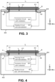
- FIG. 3 shows a semiconductor substrate 300 with a soft-magnetic component 311 and with electromagnetic transducers (in the example of FIG. 3 : two horizontal Hall elements, H1, H2) arranged near ends of the (e.g. elongated shaped) soft-magnetic component 311 or near the periphery of the (e.g. circular shaped) soft-magnetic component 311, and circuitry 301, 302 for applying a modulated signal to the soft magnetic component 311, and circuitry 307 for reading and demodulating signals obtained from the electromagnetic transducers H1, H2.
- the soft-magnetic component 311 is primarily used to guide flux lines, but its permeability is varied.
- the readout circuit 307 with demodulator is configured for demodulating the signals obtained from the transducers, e.g. the Hall elements H1, H2.
- the demodulation is synchronous with the modulation, e.g. using a same clock reference (not explicitly shown).
- the modulation is not fixed, but e.g. one or more of the frequency, the amplitude, the duty cycle, the dc component of modulation signal is varied.
- FIG. 4 shows a semiconductor substrate 400 which can be seen as a variant of FIG. 3 , further comprising a sensing circuit 402 for measuring and demodulating a response signal obtained from the soft-magnetic component 411.
- This soft-magnetic component may for example be designed (material and shape and size) as an MR element or as an MI element.
- the readout circuit 407 and the Hall elements H1, H2 are omitted.
- the readout circuit 407 and the Hall elements H1, H2 are present, and this same soft-magnetic component 411 is also used as a flux-guide for guiding flux lines to the electromagnetic transducers H1, H2 (e.g. horizontal Hall elements).
- the Hall elements H1, H2 may be read-out while the excitation circuit 401 is disabled or disconnected from the soft-magnetic component.
- the Hall elements H1, H2 may be read-out while the excitation circuit 401 is active and applying a modulated signal to the soft-magnetic material, to thereby modulate its magnetic sensitivity.
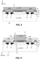
- FIG. 5 shows a cross-sectional view of a semiconductor device 500, e.g. a CMOS substrate, with a soft-magnetic component 511 electrically connected to circuitry of the semiconductor substrate 500 via openings 516a, 516b through a polyimide layer 554 on top of which the soft-magnetic element 511 is situated.
- each opening 516a, 516b accommodates an excitation contact E1, E2 and a sense contact S1, S2.
- the opening is substantially filled with the soft-magnetic material.
- This technique may be used to provide a soft-magnetic component having "back contacts" or “bottom contacts", not only for an MI-component, but also for a passive soft-magnetic component (e.g. a disk shaped IMC), or a soft-magnetic core of an integrated transformer, or the soft-magnetic core of an integrated fluxgate, e.g. for enabling detection of a mechanical problem (e.g. broken or peeled off).
- a mechanical problem
- FIG. 5 The main purpose of FIG. 5 is to show how a soft-magnetic component 511 can be electrically connected to circuitry of a semiconductor substrate by means of "back contacts".
- the semiconductor substrate 500 may be based on a CMOS device with a passivation layer 552 and with contact pads 551.
- a buffer layer 554 e.g. a polyimide layer is applied; a first relative large opening 516a is made in the buffer layer above the contact pads E1, 51, and a second relatively large opening 516b is made in the buffer layer above the contact pads E2, S2, and four relatively small openings are made to expose the contact pads 551.
- a conductive seed layer 555 may be sputtered, and a soft magnetic material (e.g.
- FeNi or a FeNi alloy may be applied on top of the seed layer, e.g. by electroplating.
- the relatively large openings are thus mainly filled with the soft-magnetic material 511, and the soft-magnetic component 511 thus formed, has four "back contacts" or "bottom contacts”.
- the contact pads 511 are made by the CMOS process (with high position accuracy), and that the position tolerances of the opening 516a, 516b through the buffer layer 554 can be relaxed.
- any of the circuits shown FIG. 1 to FIG. 4 can be used, and other components, such as e.g. Hall plates or coils may also be added, e.g. planar coils under the soft-magnet component, or coils wound around the soft-magnetic component (e.g. using electrical tracks underneath and bond wires above).
- other components such as e.g. Hall plates or coils may also be added, e.g. planar coils under the soft-magnet component, or coils wound around the soft-magnetic component (e.g. using electrical tracks underneath and bond wires above).
- the soft-magnetic component 511 is a circular disk
- the semiconductor substrate further comprises a plurality of horizontal Hall elements arranged near the periphery of that disk, for example, as also illustrated in FIG. 12 to FIG. 17B and FIG. 19 .
- the sensor contact 51 coincides with the excitation contact E1
- the sensor contact S2 coincides with the excitation contact E2.
- FIG. 6 shows a semiconductor substrate 600, e.g. a CMOS substrate with electronic circuitry (not shown in FIG. 6 , but see e.g. FIG. 1 to FIG. 4 and FIG. 7 to FIG. 10 , etc.), and with a soft-magnetic component 611 electrically connected to said circuitry of the semiconductor substrate via "side-contacts".
- the substrate 600 of FIG. 6 can be seen as a variant of the substrate 500 of FIG. 5 .
- the semiconductor substrate 600 may be based on a CMOS device with a passivation layer 652 and with contact pads 651.
- a buffer layer 654 e.g. a polyimide layer is applied; a first relative large opening 616a, 616b is made in the buffer layer 654 above the contact pads E1, 51, and a second relatively large opening is made in the buffer layer 654 above the contact pads E2, S2, and four relatively small openings are made to expose the contact pads 651.
- a conductive seed layer 655 may be sputtered.
- the soft magnetic material is not applied yet, but first a mask is applied to cover a region between the two relatively large openings 616a, 616b, and the openings are mainly filled with a conductive material, such as e.g. copper (Cu). Then the material in the intermediate region is removed, and a soft magnetic material (e.g. FeNi or a FeNi alloy) is applied, on top of the seed layer, e.g. by electroplating.
- the relatively large openings are thus mainly filled with the non-magnetic material (e.g. Cu), and the soft-magnetic component 611 thus formed may have two or more side contact surfaces 656a, 656b. In this way, the direction of a current flowing through the soft-magnetic material in some embodiments of the present invention, can be better controlled, and the current can be made more uniform.
- the sensing contact 51 may coincide with the excitation contact E1
- the sensing contact S2 may coincide with the excitation contact E2.
- FIG. 7 is a schematic representation of a semiconductor device 750 having a soft magnetic component 711, and an excitation circuit 701 and a sensing circuit 702, and a processing circuit 706, the device being configured for detecting (e.g. in a diagnostic mode) a defect of the soft-magnetic component, e.g. broken or (partially) peeled off.
- This diagnostic function can be added to any existing semiconductor device having an active or passive soft-magnetic component, e.g. can be added to any of the circuits of FIG. 2 to FIG. 4 and variants thereof.
- the soft-magnetic component may be any one of an MR element, an MI element, an IMC, an integrated fluxgate, a magnetic core of an integrated transformer, etc.
- the excitation circuit may be configured to generate a DC signal or an AC signal.
- the processing circuit 706 may be configured to output a signal indicative of the defect.
- an electrical resistance or an impedance of the soft-magnetic component is compared with a predefined threshold value, and if the resistance or impedance is larger than the threshold value, an error is detected.
- This fault-detection may not be the sole function of the semiconductor device. Indeed, the semiconductor device may have multiple modes of operation, may have additional circuitry, and may have additional components, such as e.g. two or more Hall elements near a periphery of the soft-magnetic component 711, or such as e.g. two or more coils arranged near or around the soft-magnetic component 711.
- the processing circuit may also output another signal or value, e.g. an impedance, a magnetic field value, a current, a torque, a linear or angular position.
- the first sensing contact 51 may coincide with the first excitation contact E1
- the second sensing contact S2 may coincide with the second excitation contact E2.
- the contacts may be implemented as "back contacts” and/or “side contacts”, e.g. as illustrated in FIG. 5 and/or FIG. 6 .
- FIG. 7 may be seen as a variant or a more detailed version of FIG. 1 and FIG. 2 , and as a subset of FIG. 4 .
- FIG. 8 shows a semiconductor device 850, which can be seen as a variant of the semiconductor device 750 of FIG. 7 .
- the device 850 further comprises one or more electromagnetic transducers T1, T2 (e.g. Hall elements or coils) arranged in the vicinity of the soft-magnetic component 811, and operatively connected thereto.
- T1, T2 e.g. Hall elements or coils
- the soft-magnetic component 811 is an IMC
- the transducers are Horizontal Hall elements arranged near a periphery of the IMC.
- the "energizing and readout circuit” 807 is typically referred to as a "biasing and readout” circuit.
- the semiconductor substrate may comprise more than two Horizontal Hall elements as also illustrated e.g. in FIG. 15, FIG. 16 , FIG. 19 , FIG. 20 .
- the soft-magnetic component 811 is an integrated fluxgate
- the transducers T1, T2 are coils, e.g. spiral coils arranged near opposite ends of the soft-magnetic component 811, or coils wrapped around the soft-magnetic component.
- the "energizing and readout circuit” 807 may also be referred to as “transmitter circuit” and "receiver circuit”.
- the first coil T1 may be referred to as "excitation coil”
- the second coil T2 may be referred to as "pick-up coil”
- the third (optional) coil T3 may be referred to as "biasing coil”.
- This semiconductor device 850 may have two modes of operation, e.g. a first mode (e.g. diagnostic mode) for detecting a defect of the soft-magnetic component 811 mainly using the circuits 801 and 802; and a second mode wherein the soft-magnetic component may be left floating, while signals are obtained from the transducers T1, T2.
- a first mode e.g. diagnostic mode
- a second mode wherein the soft-magnetic component may be left floating, while signals are obtained from the transducers T1, T2.
- FIG. 9 shows a semiconductor device 950, which can be seen as a variant of the semiconductor device 850 of FIG. 8 , wherein the sensing contacts S1, 52 coincide with the excitation contacts E1, E2 respectively, and wherein the semiconductor device 950 further comprises a modulator for modulating the magnetic permeability of the soft-magnetic material, e.g. as part of the excitation circuit 901, and further comprises a demodulator 917, e.g. following the readout circuit 907 for demodulating the signals obtained from the one or more electromagnetic transducers T1, T2.
- the modulation may be AM modulation or FM modulation, or other suitable types of modulation.
- Preferably "synchronous demodulation" is used.
- the sensing circuit 802 of FIG. 8 may be present (e.g. for detecting a defect of the soft-magnetic component), or may be omitted.
- the soft-magnetic component 911 may be an IMC and the transducers T1, T2 may be horizontal Hall elements. In another specific example, the soft-magnetic component 911 may be an integrated fluxgate and the transducers T1, T2 may be coils.
- FIG. 10 shows a semiconductor device 1050, which can be seen as another variant of the semiconductor device 850 of FIG. 8 , wherein the semiconductor device 1050 further comprises a modulator for modulating the magnetic permeability of the soft-magnetic component 1011, e.g. as part of the excitation circuit 1001, and further comprises a demodulator 1017, e.g. following the sensing circuit 1002 for demodulating the signals obtained from the sensing circuit 1002.
- the one or more electromagnetic transducers T1, T2 and the "energizing and readout circuit" 807 of FIG. 8 may be present, or may be omitted.
- the soft-magnetic component 1011 may be a magneto-resistive (MR) component or a magneto-inductive (MI) component, e.g. having an elongated shape.
- the optional horizontal Hall elements may be located near the ends of the soft-magnetic component.
- the output signal provided by the processing circuit 1006 may be related to a magnetic field strength measured by the soft-magnetic component 1011.
- FIG. 11(a) shows a top view
- FIG. 11(b) shows a side view of an example or a variant of FIG. 8
- the sensing contacts S1, 52 coincide with the excitation contacts E1, E2 respectively
- the soft-magnetic component 1111 is a magneto-inductive (MI) element having an elongated shape extending in a direction X parallel to the substrate, and wherein two horizontal Hall elements are located near the longitudinal ends of the MI-element 1111.
- MI magneto-inductive
- a processing circuit is not explicitly shown in FIG. 11(a) and FIG. 11(b) , but see e.g. FIG. 7 to FIG. 10 .
- the semiconductor device 1150 may have various modes of operation, such as one or more, two or more, or all three of the following:
- the semiconductor substrate 1100 further comprises a modulator and a demodulator, e.g. arranged as illustrated in FIG. 3, FIG. 4 , or FIG. 10 .
- a semiconductor device may offer:
- Embodiments of the present invention may implement one ore more or all of these five modes of operation.
- FIG. 12(a) shows a top view
- FIG. 12(b) shows a side view of a semiconductor device 1250 which is a variant of the semiconductor device 1150 shown in FIG. 11(a) and FIG. 11(b)
- the soft-magnetic component 1211 is an integrated magnetic field concentrator (IMC) having a disk shape, and wherein two horizontal Hall elements H1, H2 are located near a periphery of the IMC, 180° spaced apart.
- IMC integrated magnetic field concentrator
- a processing circuit is not explicitly shown in FIG. 12(a) and FIG. 12(b) , but see e.g. FIG. 7 to FIG. 10 .
- the semiconductor device 1250 may have various modes of operation, such as one or more of the following:
- the semiconductor substrate 1200 further comprises a modulator and a demodulator, e.g. arranged as illustrated in FIG. 3, FIG. 4 , or FIG. 9 .
- a modulator and a demodulator e.g. arranged as illustrated in FIG. 3, FIG. 4 , or FIG. 9 .
- Such a device may have: iii) a third mode of operation, in which the magnetic permeability of the IMC 1211 is modulated, and the signals h1, h2 obtained from the Hall elements H1, H2 are demodulated.
- FIG. 13 is a simplified representation of a semiconductor device 1250 as illustrated in FIG. 12(a) and FIG. 12(b) or variants thereof, having two electrical contacts c1, c2 and two Horizontal Hall elements H1, H2, angularly spaced by 180°.
- the Hall elements H1, H2 are located at a first radial distance from the centre of the disk.
- the electrical contacts c1, c2 are located at a second radial distance from the centre of the disk, smaller than the first radial distance.
- each contact c1, c2 is arranged in close vicinity of a corresponding Hall element.
- the contacts c1, c2 are arranged on a virtual line interconnecting the two Hall elements, but the present invention is not limited thereto, as that is not absolutely required to detect a defect.
- FIG. 14 shows a variant of FIG. 13 , where the electrical contacts c1, c2 are also located at a second radius smaller than the first radius, but the angular positions of the electrical contacts are angularly offset by an angle ⁇ from the angular positions of the corresponding horizontal Hall elements.
- FIG. 15 shows another variant of FIG. 13 , wherein four horizontal Hall elements H1 to H4 are arranged near the periphery of the disk shaped soft-magnetic component, and are angularly spaced by multiples of 90°, and wherein four electrical contacts c1 to c4 are arranged on a second radius smaller than the first radius, and wherein each electrical contact is arranged in close proximity to a corresponding Hall element.
- the contacts may be excited and sensed in a pairwise manner, e.g. by applying at a first moment in time, a voltage between c1 and c2, while leaving c3 and c4 floating (disconnected), and measuring a resulting first current, and comparing the first current with a predefined threshold value,; and by applying at a second moment in time, a voltage between c3 and c4, while leaving c1 and c2 floating (disconnected), and measuring a resulting second current, and comparing the second current with the predefined threshold value, and detecting a defect if one or both of the first and second current is lower than the predefined threshold.
- the present invention is not limited to this particular scheme, and other schemes are possible as well, for example by applying a voltage between c1 and c3 at a first moment in time, and by applying a voltage between c2 and c4 at a second moment in time, and comparing the resulting currents with said predefined threshold value.
- the number of contacts is equal to the number of Hall elements, but that is not absolutely required, and in other embodiments, the number of contacts may be higher or lower than the number of Hall elements, as long as there are at least two contacts.
- the contacts are all located at the same radial distance, and are angularly spaced uniformly, but that is not absolutely required for the invention to work.
- the soft-magnetic component of FIG. 18 furthermore comprises two electrical contacts c1, c2, and the semiconductor substrate 1800 further comprises a test-circuit for detecting a defect of the soft-magnetic component, e.g. similar to the test circuit of FIG. 11 and FIG. 12 .
- the method may further comprise step g) of flowing a relatively strong electrical current during through the soft-magnetic component during a relatively short time-period, for creating an easy axis.
- FIG. 22 shows a flow chart of a method 2230 of manufacturing a semiconductor substrate, or a semiconductor device (e.g. a sensor device) comprising such a semiconductor substrate.
- the method of FIG. 22 can be seen as a special case of the method of FIG. 21 , wherein the soft-magnetic material is connected with circuitry of the semiconductor substrate via "back contacts" or "bottom contacts”.
- the method 2230 comprises the following steps:
- step 2233 and step 2237 are typically used in a CMOS process to form a bonding pad in the top metal of the "metal stack” (also known as “interconnection stack”).
- the bonding pad would then be routed to circuitry of the semiconductor substrate using the metal layers of the "metal stack”.
- FIG. 23 shows a flow chart of a method 2330 of manufacturing a semiconductor substrate, or a semiconductor device (e.g. a sensor device) comprising such a semiconductor substrate.
- the method of FIG. 23 can be seen as a special case of the method of FIG. 21 , wherein the soft-magnetic material is connected with circuitry of the semiconductor substrate via "back contacts" or "bottom contacts”.
- the method 2230 comprises the following steps:
Landscapes
- Physics & Mathematics (AREA)
- Condensed Matter Physics & Semiconductors (AREA)
- General Physics & Mathematics (AREA)
- Engineering & Computer Science (AREA)
- Manufacturing & Machinery (AREA)
- Chemical & Material Sciences (AREA)
- Nanotechnology (AREA)
- Hall/Mr Elements (AREA)
Priority Applications (4)
| Application Number | Priority Date | Filing Date | Title |
|---|---|---|---|
| EP22217445.0A EP4394418A1 (fr) | 2022-12-31 | 2022-12-31 | Dispositif semi-conducteur à composant magnétique doux intégré et son procédé de production |
| PCT/EP2023/087284 WO2024141406A1 (fr) | 2022-12-31 | 2023-12-21 | Dispositif à semi-conducteur avec composant magnétique doux intégré et son procédé de production |
| US18/392,467 US20240224815A1 (en) | 2022-12-31 | 2023-12-21 | Semiconductor device with integrated soft-magnetic component, and method of producing same |
| CN202380089765.4A CN120500642A (zh) | 2022-12-31 | 2023-12-21 | 具有集成软磁组件的半导体设备及其生产方法 |
Applications Claiming Priority (1)
| Application Number | Priority Date | Filing Date | Title |
|---|---|---|---|
| EP22217445.0A EP4394418A1 (fr) | 2022-12-31 | 2022-12-31 | Dispositif semi-conducteur à composant magnétique doux intégré et son procédé de production |
Publications (1)
| Publication Number | Publication Date |
|---|---|
| EP4394418A1 true EP4394418A1 (fr) | 2024-07-03 |
Family
ID=84785282
Family Applications (1)
| Application Number | Title | Priority Date | Filing Date |
|---|---|---|---|
| EP22217445.0A Pending EP4394418A1 (fr) | 2022-12-31 | 2022-12-31 | Dispositif semi-conducteur à composant magnétique doux intégré et son procédé de production |
Country Status (4)
| Country | Link |
|---|---|
| US (1) | US20240224815A1 (fr) |
| EP (1) | EP4394418A1 (fr) |
| CN (1) | CN120500642A (fr) |
| WO (1) | WO2024141406A1 (fr) |
Families Citing this family (2)
| Publication number | Priority date | Publication date | Assignee | Title |
|---|---|---|---|---|
| EP4394417A1 (fr) * | 2022-12-31 | 2024-07-03 | Melexis Technologies SA | Dispositif de capteur avec circuit et composant intégré pour mesure de magnéto-impédance, et son procédé de production |
| CN118973368B (zh) * | 2024-10-18 | 2025-03-04 | 苏州矩阵光电有限公司 | 一种霍尔芯片、霍尔传感器及检测磁场分量的方法 |
Citations (8)
| Publication number | Priority date | Publication date | Assignee | Title |
|---|---|---|---|---|
| US20120299587A1 (en) * | 2011-05-26 | 2012-11-29 | Honeywell International Inc. | Three-axis magnetic sensors |
| WO2015189023A1 (fr) * | 2014-06-13 | 2015-12-17 | Robert Bosch Gmbh | Système capteur de champ magnétique, son procédé de fabrication et son procédé de fonctionnement |
| CN109212440A (zh) * | 2018-10-31 | 2019-01-15 | 中国科学技术大学 | 一种基于固态自旋的磁场测量方法及装置和磁场测量系统 |
| US20200124686A1 (en) * | 2017-07-21 | 2020-04-23 | Asahi Intecc Co., Ltd. | Ultra-small and high-sensitivity magnetic sensor |
| US20200217908A1 (en) * | 2017-04-05 | 2020-07-09 | MultiDimension Technology Co., Ltd. | Modulated magnetoresistive sensor |
| US20200371168A1 (en) * | 2019-05-24 | 2020-11-26 | Melexis Technologies Sa | Semiconductor Device with Embedded Magnetic Flux Concentrator |
| US20210103009A1 (en) * | 2018-01-30 | 2021-04-08 | MultiDimension Technology Co., Ltd. | Three-axis upstream-modulated low-noise magnetoresistive sensor |
| EP3961926A1 (fr) | 2020-08-31 | 2022-03-02 | Melexis Bulgaria Ltd. | Dispositif et système de capteur de proximité |
Family Cites Families (2)
| Publication number | Priority date | Publication date | Assignee | Title |
|---|---|---|---|---|
| KR100590211B1 (ko) * | 2002-11-21 | 2006-06-15 | 가부시키가이샤 덴소 | 자기 임피던스 소자, 그를 이용한 센서 장치 및 그 제조방법 |
| JP6186879B2 (ja) * | 2013-05-20 | 2017-08-30 | Tdk株式会社 | 薄膜磁性素子 |
-
2022
- 2022-12-31 EP EP22217445.0A patent/EP4394418A1/fr active Pending
-
2023
- 2023-12-21 WO PCT/EP2023/087284 patent/WO2024141406A1/fr not_active Ceased
- 2023-12-21 US US18/392,467 patent/US20240224815A1/en active Pending
- 2023-12-21 CN CN202380089765.4A patent/CN120500642A/zh active Pending
Patent Citations (8)
| Publication number | Priority date | Publication date | Assignee | Title |
|---|---|---|---|---|
| US20120299587A1 (en) * | 2011-05-26 | 2012-11-29 | Honeywell International Inc. | Three-axis magnetic sensors |
| WO2015189023A1 (fr) * | 2014-06-13 | 2015-12-17 | Robert Bosch Gmbh | Système capteur de champ magnétique, son procédé de fabrication et son procédé de fonctionnement |
| US20200217908A1 (en) * | 2017-04-05 | 2020-07-09 | MultiDimension Technology Co., Ltd. | Modulated magnetoresistive sensor |
| US20200124686A1 (en) * | 2017-07-21 | 2020-04-23 | Asahi Intecc Co., Ltd. | Ultra-small and high-sensitivity magnetic sensor |
| US20210103009A1 (en) * | 2018-01-30 | 2021-04-08 | MultiDimension Technology Co., Ltd. | Three-axis upstream-modulated low-noise magnetoresistive sensor |
| CN109212440A (zh) * | 2018-10-31 | 2019-01-15 | 中国科学技术大学 | 一种基于固态自旋的磁场测量方法及装置和磁场测量系统 |
| US20200371168A1 (en) * | 2019-05-24 | 2020-11-26 | Melexis Technologies Sa | Semiconductor Device with Embedded Magnetic Flux Concentrator |
| EP3961926A1 (fr) | 2020-08-31 | 2022-03-02 | Melexis Bulgaria Ltd. | Dispositif et système de capteur de proximité |
Non-Patent Citations (1)
| Title |
|---|
| ANONYMOUS: "Magnetic sensor", RESEARCH DISCLOSURE, KENNETH MASON PUBLICATIONS, HAMPSHIRE, UK, GB, vol. 413, no. 37, 1 September 1998 (1998-09-01), XP007123252, ISSN: 0374-4353 * |
Also Published As
| Publication number | Publication date |
|---|---|
| CN120500642A (zh) | 2025-08-15 |
| US20240224815A1 (en) | 2024-07-04 |
| WO2024141406A1 (fr) | 2024-07-04 |
Similar Documents
| Publication | Publication Date | Title |
|---|---|---|
| US12061246B2 (en) | Method and apparatus for magnetic sensor producing a changing magnetic field | |
| JP6018093B2 (ja) | 単一パッケージブリッジ型磁界角度センサ | |
| JP6438959B2 (ja) | 単一チップz軸線形磁気抵抗センサ | |
| EP2752675B1 (fr) | Capteur de champ magnétique à axe triple mtj et son procédé d'encapsulation | |
| US20240224815A1 (en) | Semiconductor device with integrated soft-magnetic component, and method of producing same | |
| US10495699B2 (en) | Methods and apparatus for magnetic sensor having an integrated coil or magnet to detect a non-ferromagnetic target | |
| CN102656471B (zh) | 磁场传感器、使用其的磁场测定方法、电力测量装置及电力测量方法 | |
| JP5965924B2 (ja) | プッシュプル型ブリッジ磁気抵抗センサ | |
| EP2667213A1 (fr) | Capteur de champ magnétique du type à pont à boîtier indépendant | |
| US6472868B1 (en) | Magnetic impedance element having at least two thin film-magnetic cores | |
| JPWO2011155527A1 (ja) | フラックスゲートセンサおよびそれを利用した電子方位計ならびに電流計 | |
| JP5620076B2 (ja) | 電力計測装置 | |
| US12013419B2 (en) | Integrated current sensor with magnetic flux concentrators | |
| US20240219487A1 (en) | Sensor device with circuit and integrated component for magneto-impedance measurement, and method of producing same | |
| Liakopoulos et al. | A micro fluxgate magnetic sensor using micromachined 3-dimensional planar coils | |
| JP2012073034A (ja) | 電力計測装置および電力計測方法 | |
| WO2011155526A1 (fr) | Capteur de sonde magnétométrique, radiogoniomètre électronique l'utilisant et ampèremètre |
Legal Events
| Date | Code | Title | Description |
|---|---|---|---|
| PUAI | Public reference made under article 153(3) epc to a published international application that has entered the european phase |
Free format text: ORIGINAL CODE: 0009012 |
|
| STAA | Information on the status of an ep patent application or granted ep patent |
Free format text: STATUS: THE APPLICATION HAS BEEN PUBLISHED |
|
| AK | Designated contracting states |
Kind code of ref document: A1 Designated state(s): AL AT BE BG CH CY CZ DE DK EE ES FI FR GB GR HR HU IE IS IT LI LT LU LV MC ME MK MT NL NO PL PT RO RS SE SI SK SM TR |
|
| STAA | Information on the status of an ep patent application or granted ep patent |
Free format text: STATUS: REQUEST FOR EXAMINATION WAS MADE |
|
| 17P | Request for examination filed |
Effective date: 20241224 |