EP4394465A2 - Procédés et appareil pour coupleur optique - Google Patents
Procédés et appareil pour coupleur optique Download PDFInfo
- Publication number
- EP4394465A2 EP4394465A2 EP23212635.9A EP23212635A EP4394465A2 EP 4394465 A2 EP4394465 A2 EP 4394465A2 EP 23212635 A EP23212635 A EP 23212635A EP 4394465 A2 EP4394465 A2 EP 4394465A2
- Authority
- EP
- European Patent Office
- Prior art keywords
- optical
- optical waveguide
- waveguide
- width
- tapered portion
- Prior art date
- Legal status (The legal status is an assumption and is not a legal conclusion. Google has not performed a legal analysis and makes no representation as to the accuracy of the status listed.)
- Pending
Links
Images



Classifications
-
- G—PHYSICS
- G02—OPTICS
- G02B—OPTICAL ELEMENTS, SYSTEMS OR APPARATUS
- G02B6/00—Light guides; Structural details of arrangements comprising light guides and other optical elements, e.g. couplings
- G02B6/24—Coupling light guides
- G02B6/26—Optical coupling means
- G02B6/30—Optical coupling means for use between fibre and thin-film device
- G02B6/305—Optical coupling means for use between fibre and thin-film device and having an integrated mode-size expanding section, e.g. tapered waveguide
-
- G—PHYSICS
- G02—OPTICS
- G02B—OPTICAL ELEMENTS, SYSTEMS OR APPARATUS
- G02B6/00—Light guides; Structural details of arrangements comprising light guides and other optical elements, e.g. couplings
- G02B6/10—Light guides; Structural details of arrangements comprising light guides and other optical elements, e.g. couplings of the optical waveguide type
- G02B6/12—Light guides; Structural details of arrangements comprising light guides and other optical elements, e.g. couplings of the optical waveguide type of the integrated circuit kind
- G02B6/122—Basic optical elements, e.g. light-guiding paths
- G02B6/1228—Tapered waveguides, e.g. integrated spot-size transformers
-
- G—PHYSICS
- G02—OPTICS
- G02B—OPTICAL ELEMENTS, SYSTEMS OR APPARATUS
- G02B6/00—Light guides; Structural details of arrangements comprising light guides and other optical elements, e.g. couplings
- G02B6/10—Light guides; Structural details of arrangements comprising light guides and other optical elements, e.g. couplings of the optical waveguide type
- G02B6/12—Light guides; Structural details of arrangements comprising light guides and other optical elements, e.g. couplings of the optical waveguide type of the integrated circuit kind
- G02B2006/12133—Functions
- G02B2006/12147—Coupler
-
- G—PHYSICS
- G02—OPTICS
- G02B—OPTICAL ELEMENTS, SYSTEMS OR APPARATUS
- G02B6/00—Light guides; Structural details of arrangements comprising light guides and other optical elements, e.g. couplings
- G02B6/10—Light guides; Structural details of arrangements comprising light guides and other optical elements, e.g. couplings of the optical waveguide type
- G02B6/12—Light guides; Structural details of arrangements comprising light guides and other optical elements, e.g. couplings of the optical waveguide type of the integrated circuit kind
- G02B2006/12166—Manufacturing methods
- G02B2006/12195—Tapering
Definitions
- the present application relates to optical edge couplers, and in particular to edge couplers for optical signal communication.
- an optical edge coupler with two waveguides formed within one cladding layer of the coupler configured to function as a single transformer, where the two waveguides are configured with unique profiles that may improve the mode overlap between the coupler and the optical fibres having small or medium (i.e. ⁇ 8 ⁇ m) MFDs.
- the coupler disclosed herein may be extended to mode match with SMF28 fibres.
- the present disclosure provides a one-layer optical edge coupler that is suited for a one-step fabrication process, hence lowering fabrication and device cost.
- the present disclosure provides an adiabatic optical edge coupler with reduced levels of insertion loss.
- a method of optically coupling a light source and an optical circuit comprising: receiving an input optical mode from the light source at a chip facet of an optical coupler by a first optical waveguide and a second optical waveguide; causing an optical mode to be optically coupled between the first optical waveguide and the second optical waveguide; transforming the optical mode onto the first waveguide over a first tapered portion of the second waveguide; and decoupling the optical mode from the second waveguide over a second tapered portion of the second waveguide.
- the first waveguide may widen from a first tip width at the facet to a first terminating width at a terminal end.
- the first tip width may be substantially equal to the second tip width.
- each of the first optical waveguide and the second optical waveguide may further comprise an extension portion, respectively.
- the extension portion of each of the first and second waveguide may be of uniform width.
- one or more of the transverse distance, the first tip width, and the second tip width may be configured to mode match with an external light source optically connected to the optical coupler at the facet.
- the first optical waveguide and the second optical waveguide may be ribbed waveguides.
- the second tapered portion may have a length of at least 4% of a total length of the second waveguide.
- the second optical waveguide may further comprise a radiation tip extending from the second tapered portion, the radiation tip is configured to reduce optical reflections within the second optical waveguide.
- the radiation tip may be configured with one or more of a curved profile and a narrowing tip.
- the first waveguide may be configured with a first tapering angle; the first tapered portion may be configured with a second tapering angle; and the second tapered portion may be configured with a third tapering angle.
- the first tapering angle may be greater than the second tapering angle.
- the first tapering angle, the second tapering angle, and the third tapering angle may be one of a constant tapering angle, a polynomial tapering angle, and a discrete step tapering angle.
- Any one of the above aspects may further comprise reducing reflections in the second waveguide with a radiation tip that extends from the second tapered portion.
- Any one of the above aspects may further comprise configuring one of a gap distance between the first waveguide and the second waveguide at the chip facet, a first width of the first waveguide at the chip facet, and a second width of the second waveguide at the chip facet for mode matching with the light source.
- any one of the above aspects may further comprise configuring the first tapered portion to extend from a first width to a second width; configuring the second tapered portion to extend from the second width to a third width; and configuring the second width based on one or more of a total length of the second optical waveguide, a gap distance between the first and the second optical waveguides at the chip facet, and tip widths of the first and second optical waveguides at the chip facet.
- Any one of the above aspects may further comprise configuring the first tapering angle, the second tapering angle, and the third tapering angle as one of a constant tapering angle, a polynomial tapering angle, and a discrete step tapering angle.
- Silicon photonics in the implementation of photonic integrated circuits has gained increasing traction as a viable technology, particularly in the area of quantum computing, due to its technological maturity, low fabrication cost, high integration density, and compatibility with existing fabrication methodologies.
- PIC photonic integrated circuits
- the size of PIC elements has been greatly reduced, resulting in higher integration density.
- external optical sources such as fibre cables and integrated waveguides
- Mode matching may be especially challenging for systems having high or medium refractive index contrast between the waveguide and surrounding cladding material, which may be desired to achieve total internal reflection of the optical signal.
- optical edge couplers configured to facilitate optical communication between an external light source (e.g. fibre optical cable or laser source) and an integrated silicon waveguide at a high optical efficiency becomes a crucial design element in any integrated silicon photonic system.
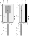
- FIGS. 1A and 1B illustrate a cross-sectional top view and a cross-sectional side view of an exemplary photonic optical system 100, respectively.
- Photonic optical system 100 includes a PIC 110.
- the PIC 110 may be any device that integrates, typically by processes of semiconductor fabrication, one or more photonic components configured to perform certain photonic functionalities onto a semiconductor or dielectric substrate.
- the PIC 110 is configured to process information that is imposed onto optical beams that typically have wavelengths ranging from the UV spectrum to the infrared spectrum.
- the photonic system 100 may include two or more such layers.
- the cladding layer 114 may be fabricated with any suitable cladding material, such as SiO2, SiN, and gallium aluminum arsenide (GaAlAs) for example.
- the PIC 110 which includes one or more functional optical elements such as modulators, switches, and detectors (not shown), may be formed in the cladding layer 114 by any suitable means such as etching (mechanical or chemical), engraving, and/or lithography into the upper surface of the cladding layer 114.
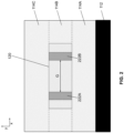
- FIG. 2 illustrates a partial elevation view of the chip facet 118 from the A-A line in FIG. 1B showing the chip facet 118 in accordance with an exemplary embodiment of the present disclosure.
- the optical coupler 120 includes two waveguides 222A and 222B (collectively referred to as waveguides 222) that are fabricated into the cladding layer 114B, which is supported above a cladding layer 114A formed immediately above substrate 112.
- the waveguides 222 are arranged substantially parallel to each other within the layer 114B separated by a transverse distance G along the x-axis.
- the cladding layers 114 may be of any suitable cladding material so as to provide contrasting refractive indices with the material of the waveguides 222 such that the coupled mode transmitted within the optical coupler is optically confined by means of total internal reflection.
- the cladding layers 114 may be any of SiO2 and GaAIAs.
- the optical waveguides 222 may, for example, be fabricated from SiN, silicon oxynitride, air, silicon, barium titanate, lithium niobate, indium gallium arsenide phosphide (InGaAsP), gallium arsenide (GaAs), or any suitable material to achieve total internal reflection with the selected cladding material.
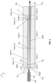
- region 1 is defined as the portion of optical coupler 420 where the coupled optical mode between the waveguides 422 is formed.
- both waveguides 422A and 422B are characterized by having respective extension portions 402A and 402B (collectively referred to as extension portions 402) that extend from the chip facet 118 to a plane 1-2 (the plane parallel to the xy-plane between region 1 and region 2).
- FIG. 4 shows an embodiment where the extension portions 402 are flush with the chip facet 118. In other embodiments where the extension portions 402 are recessed from the chip facet 118, region 1 may be preceded by a segment of cladding material.
- the waveguide 422B extends from the chip facet 118 to an integrated routing waveguide of the PIC 110 (not shown), and thus serves as the main routing waveguide that is responsible for transmitting the optical mode from the facet 118 to the PIC 110.
- Waveguide 422B includes a widening region having an inversely tapered profile that expands from a first width WB1 at plane 1-2 to a second terminating width WB2 at the opposing end of the optical coupler 420.
- the tapering angle is continuous and uniform.
- the tapering may be in the form of discrete steps, polynomial order tapering, and other suitable types of tapering profile.
- Region 4 also referred to as the anti-reflection region, is an optional region that may be incorporated to reduce any possible reflections due to waveguide terminations in region 3. In particular, a large termination width WA3 could lead to signal reflections that may increase optical loss.
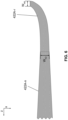
- Region 4 is characterized by waveguide 422A having an optional radiation tip 422A-r which is better illustrated in FIG. 6 .
- the anti-reflection properties of the radiation tip 422A-r may be achieved by having a curved profile and/or narrowing towards a smaller tip width WA4.
- the embodiment in FIG. 6 shows a curved radiation tip 422A-r narrowing from the terminating width WA3 at plane 3-4 to a tip width of WA4, where WA4 ⁇ WA3.
- region 5 may be less than 5-10% of the total structure length, however, in some cases of slow tapering, region 5 can be 10-70% of the total structure length, particularly in cases where a slightly multimode or multimode waveguide is expected at WB2.
- FIG. 7 shows a flowchart for a method of optically coupling a light source and an integrated optical circuit in accordance with embodiments of the present disclosure.
- signal reflections, possibly due to improper termination, within the second waveguide may be reduced in a radiation tip that extends from the second tapered portion.
- the reflection reduction may be realized through a curved radiation tip curving away from the first optical waveguide, a continually narrowing radiation tip that narrows from the termination width of the second waveguide to an even smaller tip width, or a combination of the two.
Landscapes
- Physics & Mathematics (AREA)
- General Physics & Mathematics (AREA)
- Optics & Photonics (AREA)
- Engineering & Computer Science (AREA)
- Power Engineering (AREA)
- Microelectronics & Electronic Packaging (AREA)
- Optical Integrated Circuits (AREA)
Applications Claiming Priority (1)
| Application Number | Priority Date | Filing Date | Title |
|---|---|---|---|
| US202263430395P | 2022-12-06 | 2022-12-06 |
Publications (2)
| Publication Number | Publication Date |
|---|---|
| EP4394465A2 true EP4394465A2 (fr) | 2024-07-03 |
| EP4394465A3 EP4394465A3 (fr) | 2024-07-17 |
Family
ID=88978489
Family Applications (1)
| Application Number | Title | Priority Date | Filing Date |
|---|---|---|---|
| EP23212635.9A Pending EP4394465A3 (fr) | 2022-12-06 | 2023-11-28 | Procédés et appareil pour coupleur optique |
Country Status (2)
| Country | Link |
|---|---|
| US (1) | US20240184043A1 (fr) |
| EP (1) | EP4394465A3 (fr) |
Family Cites Families (4)
| Publication number | Priority date | Publication date | Assignee | Title |
|---|---|---|---|---|
| JP5259829B2 (ja) * | 2009-09-28 | 2013-08-07 | 株式会社東芝 | 光結合装置及び光合分波装置 |
| US10663663B2 (en) * | 2014-02-28 | 2020-05-26 | Ciena Corporation | Spot-size converter for optical mode conversion and coupling between two waveguides |
| US11215755B2 (en) * | 2019-09-19 | 2022-01-04 | GenXComm, Inc. | Low loss, polarization-independent, large bandwidth mode converter for edge coupling |
| US11204469B1 (en) * | 2020-06-01 | 2021-12-21 | Honeywell International Inc. | Apparatus for high-efficiency fiber-to-chip coupling and mode-conversion to integrated photonics platform |
-
2023
- 2023-11-24 US US18/518,732 patent/US20240184043A1/en active Pending
- 2023-11-28 EP EP23212635.9A patent/EP4394465A3/fr active Pending
Also Published As
| Publication number | Publication date |
|---|---|
| EP4394465A3 (fr) | 2024-07-17 |
| US20240184043A1 (en) | 2024-06-06 |
Similar Documents
| Publication | Publication Date | Title |
|---|---|---|
| US8649639B2 (en) | Method and system for waveguide mode filters | |
| US7978941B2 (en) | Single mode photonic circuit architecture and a new optical splitter design based on parallel waveguide mode conversion | |
| US10345522B2 (en) | Multi-core silicon waveguide in a mode-converting silicon photonic edge coupler | |
| US11402581B2 (en) | Mode converter | |
| US8238704B2 (en) | Light coupler between an optical fiber and a waveguide made on an SOI substrate | |
| EP3117252B1 (fr) | Guide d'ondes à oxyde a arête suspendue | |
| JP5811273B2 (ja) | 光素子、光送信素子、光受信素子、ハイブリッドレーザ、光送信装置 | |
| US8948553B2 (en) | Deep-shallow optical radiation filters | |
| US12422622B2 (en) | Photonic systems comprising an asymmetric coupler and methods of fabrication | |
| JP6820671B2 (ja) | 光回路デバイスとこれを用いた光トランシーバ | |
| US12313882B2 (en) | Taper-based spot-size converter implementing intermediate optical mode converter | |
| US20050185893A1 (en) | Method and apparatus for tapering an optical waveguide | |
| KR20050074290A (ko) | 광섬유 및 평면 광학 도파관을 치밀하게 결합하는 방법 및장치 | |
| US10422957B2 (en) | Method and system for a low-loss optical Y-junction power splitter | |
| EP4394465A2 (fr) | Procédés et appareil pour coupleur optique | |
| US20230384542A1 (en) | Optical connecting structure, optical module and manufacturing method for optical connecting structure | |
| US12487400B2 (en) | Optical device, substrate type optical waveguide element, optical communication apparatus, and inter-waveguide transition method | |
| US20230296844A1 (en) | Spot size conversion apparatus and related method | |
| US20230266534A1 (en) | Optical Waveguide Device and Method for Manufacturing the Same | |
| EP4575309A1 (fr) | Guide d'ondes optique et procédé de rayonnement de lumière incliné | |
| US20240184044A1 (en) | Apparatus for optical coupler | |
| US20130156362A1 (en) | Core and optical waveguide | |
| JP2024098873A (ja) | 光デバイス、光送信装置及び光受信装置 | |
| Kim et al. | Novel ring cavity resonators incorporating total internal reflection mirrors and semiconductor optical amplifiers |
Legal Events
| Date | Code | Title | Description |
|---|---|---|---|
| PUAI | Public reference made under article 153(3) epc to a published international application that has entered the european phase |
Free format text: ORIGINAL CODE: 0009012 |
|
| STAA | Information on the status of an ep patent application or granted ep patent |
Free format text: STATUS: THE APPLICATION HAS BEEN PUBLISHED |
|
| PUAL | Search report despatched |
Free format text: ORIGINAL CODE: 0009013 |
|
| AK | Designated contracting states |
Kind code of ref document: A2 Designated state(s): AL AT BE BG CH CY CZ DE DK EE ES FI FR GB GR HR HU IE IS IT LI LT LU LV MC ME MK MT NL NO PL PT RO RS SE SI SK SM TR |
|
| AK | Designated contracting states |
Kind code of ref document: A3 Designated state(s): AL AT BE BG CH CY CZ DE DK EE ES FI FR GB GR HR HU IE IS IT LI LT LU LV MC ME MK MT NL NO PL PT RO RS SE SI SK SM TR |
|
| RIC1 | Information provided on ipc code assigned before grant |
Ipc: G02B 6/12 20060101ALN20240612BHEP Ipc: G02B 6/30 20060101ALI20240612BHEP Ipc: G02B 6/14 20060101ALI20240612BHEP Ipc: G02B 6/122 20060101AFI20240612BHEP |
|
| STAA | Information on the status of an ep patent application or granted ep patent |
Free format text: STATUS: REQUEST FOR EXAMINATION WAS MADE |
|
| 17P | Request for examination filed |
Effective date: 20250117 |
|
| STAA | Information on the status of an ep patent application or granted ep patent |
Free format text: STATUS: EXAMINATION IS IN PROGRESS |
|
| 17Q | First examination report despatched |
Effective date: 20250613 |