EP4394494A1 - Optisches laminat und herstellungsverfahren dafür, intelligentes fenster damit sowie fahrzeug und gebäudefenster oder -tür damit - Google Patents
Optisches laminat und herstellungsverfahren dafür, intelligentes fenster damit sowie fahrzeug und gebäudefenster oder -tür damit Download PDFInfo
- Publication number
- EP4394494A1 EP4394494A1 EP22861600.9A EP22861600A EP4394494A1 EP 4394494 A1 EP4394494 A1 EP 4394494A1 EP 22861600 A EP22861600 A EP 22861600A EP 4394494 A1 EP4394494 A1 EP 4394494A1
- Authority
- EP
- European Patent Office
- Prior art keywords
- polarizing plate
- transparent conductive
- conductive layer
- optical stack
- layer
- Prior art date
- Legal status (The legal status is an assumption and is not a legal conclusion. Google has not performed a legal analysis and makes no representation as to the accuracy of the status listed.)
- Withdrawn
Links
Images




Classifications
-
- G—PHYSICS
- G02—OPTICS
- G02F—OPTICAL DEVICES OR ARRANGEMENTS FOR THE CONTROL OF LIGHT BY MODIFICATION OF THE OPTICAL PROPERTIES OF THE MEDIA OF THE ELEMENTS INVOLVED THEREIN; NON-LINEAR OPTICS; FREQUENCY-CHANGING OF LIGHT; OPTICAL LOGIC ELEMENTS; OPTICAL ANALOGUE/DIGITAL CONVERTERS
- G02F1/00—Devices or arrangements for the control of the intensity, colour, phase, polarisation or direction of light arriving from an independent light source, e.g. switching, gating or modulating; Non-linear optics
- G02F1/01—Devices or arrangements for the control of the intensity, colour, phase, polarisation or direction of light arriving from an independent light source, e.g. switching, gating or modulating; Non-linear optics for the control of the intensity, phase, polarisation or colour
- G02F1/13—Devices or arrangements for the control of the intensity, colour, phase, polarisation or direction of light arriving from an independent light source, e.g. switching, gating or modulating; Non-linear optics for the control of the intensity, phase, polarisation or colour based on liquid crystals, e.g. single liquid crystal display cells
- G02F1/133—Constructional arrangements; Operation of liquid crystal cells; Circuit arrangements
- G02F1/1333—Constructional arrangements; Manufacturing methods
- G02F1/1335—Structural association of cells with optical devices, e.g. polarisers or reflectors
- G02F1/133528—Polarisers
- G02F1/133536—Reflective polarizers
-
- G—PHYSICS
- G02—OPTICS
- G02B—OPTICAL ELEMENTS, SYSTEMS OR APPARATUS
- G02B5/00—Optical elements other than lenses
- G02B5/30—Polarising elements
-
- B—PERFORMING OPERATIONS; TRANSPORTING
- B60—VEHICLES IN GENERAL
- B60J—WINDOWS, WINDSCREENS, NON-FIXED ROOFS, DOORS, OR SIMILAR DEVICES FOR VEHICLES; REMOVABLE EXTERNAL PROTECTIVE COVERINGS SPECIALLY ADAPTED FOR VEHICLES
- B60J3/00—Antiglare equipment associated with windows or windscreens; Sun visors for vehicles
- B60J3/007—Sunglare reduction by coatings, interposed foils in laminar windows, or permanent screens
-
- E—FIXED CONSTRUCTIONS
- E06—DOORS, WINDOWS, SHUTTERS, OR ROLLER BLINDS IN GENERAL; LADDERS
- E06B—FIXED OR MOVABLE CLOSURES FOR OPENINGS IN BUILDINGS, VEHICLES, FENCES OR LIKE ENCLOSURES IN GENERAL, e.g. DOORS, WINDOWS, BLINDS, GATES
- E06B9/00—Screening or protective devices for wall or similar openings, with or without operating or securing mechanisms; Closures of similar construction
- E06B9/24—Screens or other constructions affording protection against light, especially against sunshine; Similar screens for privacy or appearance; Slat blinds
-
- G—PHYSICS
- G02—OPTICS
- G02F—OPTICAL DEVICES OR ARRANGEMENTS FOR THE CONTROL OF LIGHT BY MODIFICATION OF THE OPTICAL PROPERTIES OF THE MEDIA OF THE ELEMENTS INVOLVED THEREIN; NON-LINEAR OPTICS; FREQUENCY-CHANGING OF LIGHT; OPTICAL LOGIC ELEMENTS; OPTICAL ANALOGUE/DIGITAL CONVERTERS
- G02F1/00—Devices or arrangements for the control of the intensity, colour, phase, polarisation or direction of light arriving from an independent light source, e.g. switching, gating or modulating; Non-linear optics
- G02F1/01—Devices or arrangements for the control of the intensity, colour, phase, polarisation or direction of light arriving from an independent light source, e.g. switching, gating or modulating; Non-linear optics for the control of the intensity, phase, polarisation or colour
- G02F1/13—Devices or arrangements for the control of the intensity, colour, phase, polarisation or direction of light arriving from an independent light source, e.g. switching, gating or modulating; Non-linear optics for the control of the intensity, phase, polarisation or colour based on liquid crystals, e.g. single liquid crystal display cells
- G02F1/133—Constructional arrangements; Operation of liquid crystal cells; Circuit arrangements
- G02F1/1333—Constructional arrangements; Manufacturing methods
- G02F1/1335—Structural association of cells with optical devices, e.g. polarisers or reflectors
- G02F1/133528—Polarisers
-
- G—PHYSICS
- G02—OPTICS
- G02F—OPTICAL DEVICES OR ARRANGEMENTS FOR THE CONTROL OF LIGHT BY MODIFICATION OF THE OPTICAL PROPERTIES OF THE MEDIA OF THE ELEMENTS INVOLVED THEREIN; NON-LINEAR OPTICS; FREQUENCY-CHANGING OF LIGHT; OPTICAL LOGIC ELEMENTS; OPTICAL ANALOGUE/DIGITAL CONVERTERS
- G02F1/00—Devices or arrangements for the control of the intensity, colour, phase, polarisation or direction of light arriving from an independent light source, e.g. switching, gating or modulating; Non-linear optics
- G02F1/01—Devices or arrangements for the control of the intensity, colour, phase, polarisation or direction of light arriving from an independent light source, e.g. switching, gating or modulating; Non-linear optics for the control of the intensity, phase, polarisation or colour
- G02F1/13—Devices or arrangements for the control of the intensity, colour, phase, polarisation or direction of light arriving from an independent light source, e.g. switching, gating or modulating; Non-linear optics for the control of the intensity, phase, polarisation or colour based on liquid crystals, e.g. single liquid crystal display cells
- G02F1/133—Constructional arrangements; Operation of liquid crystal cells; Circuit arrangements
- G02F1/1333—Constructional arrangements; Manufacturing methods
- G02F1/1335—Structural association of cells with optical devices, e.g. polarisers or reflectors
- G02F1/133528—Polarisers
- G02F1/133531—Polarisers characterised by the arrangement of polariser or analyser axes
-
- G—PHYSICS
- G02—OPTICS
- G02F—OPTICAL DEVICES OR ARRANGEMENTS FOR THE CONTROL OF LIGHT BY MODIFICATION OF THE OPTICAL PROPERTIES OF THE MEDIA OF THE ELEMENTS INVOLVED THEREIN; NON-LINEAR OPTICS; FREQUENCY-CHANGING OF LIGHT; OPTICAL LOGIC ELEMENTS; OPTICAL ANALOGUE/DIGITAL CONVERTERS
- G02F1/00—Devices or arrangements for the control of the intensity, colour, phase, polarisation or direction of light arriving from an independent light source, e.g. switching, gating or modulating; Non-linear optics
- G02F1/01—Devices or arrangements for the control of the intensity, colour, phase, polarisation or direction of light arriving from an independent light source, e.g. switching, gating or modulating; Non-linear optics for the control of the intensity, phase, polarisation or colour
- G02F1/13—Devices or arrangements for the control of the intensity, colour, phase, polarisation or direction of light arriving from an independent light source, e.g. switching, gating or modulating; Non-linear optics for the control of the intensity, phase, polarisation or colour based on liquid crystals, e.g. single liquid crystal display cells
- G02F1/133—Constructional arrangements; Operation of liquid crystal cells; Circuit arrangements
- G02F1/1333—Constructional arrangements; Manufacturing methods
- G02F1/1339—Gaskets; Spacers; Sealing of cells
- G02F1/13392—Gaskets; Spacers; Sealing of cells spacers dispersed on the cell substrate, e.g. spherical particles, microfibres
-
- G—PHYSICS
- G02—OPTICS
- G02F—OPTICAL DEVICES OR ARRANGEMENTS FOR THE CONTROL OF LIGHT BY MODIFICATION OF THE OPTICAL PROPERTIES OF THE MEDIA OF THE ELEMENTS INVOLVED THEREIN; NON-LINEAR OPTICS; FREQUENCY-CHANGING OF LIGHT; OPTICAL LOGIC ELEMENTS; OPTICAL ANALOGUE/DIGITAL CONVERTERS
- G02F1/00—Devices or arrangements for the control of the intensity, colour, phase, polarisation or direction of light arriving from an independent light source, e.g. switching, gating or modulating; Non-linear optics
- G02F1/01—Devices or arrangements for the control of the intensity, colour, phase, polarisation or direction of light arriving from an independent light source, e.g. switching, gating or modulating; Non-linear optics for the control of the intensity, phase, polarisation or colour
- G02F1/13—Devices or arrangements for the control of the intensity, colour, phase, polarisation or direction of light arriving from an independent light source, e.g. switching, gating or modulating; Non-linear optics for the control of the intensity, phase, polarisation or colour based on liquid crystals, e.g. single liquid crystal display cells
- G02F1/133—Constructional arrangements; Operation of liquid crystal cells; Circuit arrangements
- G02F1/1333—Constructional arrangements; Manufacturing methods
- G02F1/1339—Gaskets; Spacers; Sealing of cells
- G02F1/13398—Spacer materials; Spacer properties
-
- G—PHYSICS
- G02—OPTICS
- G02F—OPTICAL DEVICES OR ARRANGEMENTS FOR THE CONTROL OF LIGHT BY MODIFICATION OF THE OPTICAL PROPERTIES OF THE MEDIA OF THE ELEMENTS INVOLVED THEREIN; NON-LINEAR OPTICS; FREQUENCY-CHANGING OF LIGHT; OPTICAL LOGIC ELEMENTS; OPTICAL ANALOGUE/DIGITAL CONVERTERS
- G02F1/00—Devices or arrangements for the control of the intensity, colour, phase, polarisation or direction of light arriving from an independent light source, e.g. switching, gating or modulating; Non-linear optics
- G02F1/01—Devices or arrangements for the control of the intensity, colour, phase, polarisation or direction of light arriving from an independent light source, e.g. switching, gating or modulating; Non-linear optics for the control of the intensity, phase, polarisation or colour
- G02F1/13—Devices or arrangements for the control of the intensity, colour, phase, polarisation or direction of light arriving from an independent light source, e.g. switching, gating or modulating; Non-linear optics for the control of the intensity, phase, polarisation or colour based on liquid crystals, e.g. single liquid crystal display cells
- G02F1/133—Constructional arrangements; Operation of liquid crystal cells; Circuit arrangements
- G02F1/1333—Constructional arrangements; Manufacturing methods
- G02F1/1343—Electrodes
- G02F1/13439—Electrodes characterised by their electrical, optical, physical properties; materials therefor; method of making
-
- G—PHYSICS
- G02—OPTICS
- G02F—OPTICAL DEVICES OR ARRANGEMENTS FOR THE CONTROL OF LIGHT BY MODIFICATION OF THE OPTICAL PROPERTIES OF THE MEDIA OF THE ELEMENTS INVOLVED THEREIN; NON-LINEAR OPTICS; FREQUENCY-CHANGING OF LIGHT; OPTICAL LOGIC ELEMENTS; OPTICAL ANALOGUE/DIGITAL CONVERTERS
- G02F1/00—Devices or arrangements for the control of the intensity, colour, phase, polarisation or direction of light arriving from an independent light source, e.g. switching, gating or modulating; Non-linear optics
- G02F1/01—Devices or arrangements for the control of the intensity, colour, phase, polarisation or direction of light arriving from an independent light source, e.g. switching, gating or modulating; Non-linear optics for the control of the intensity, phase, polarisation or colour
- G02F1/13—Devices or arrangements for the control of the intensity, colour, phase, polarisation or direction of light arriving from an independent light source, e.g. switching, gating or modulating; Non-linear optics for the control of the intensity, phase, polarisation or colour based on liquid crystals, e.g. single liquid crystal display cells
- G02F1/137—Devices or arrangements for the control of the intensity, colour, phase, polarisation or direction of light arriving from an independent light source, e.g. switching, gating or modulating; Non-linear optics for the control of the intensity, phase, polarisation or colour based on liquid crystals, e.g. single liquid crystal display cells characterised by the electro-optical or magneto-optical effect, e.g. field-induced phase transition, orientation effect, guest-host interaction or dynamic scattering
- G02F1/139—Devices or arrangements for the control of the intensity, colour, phase, polarisation or direction of light arriving from an independent light source, e.g. switching, gating or modulating; Non-linear optics for the control of the intensity, phase, polarisation or colour based on liquid crystals, e.g. single liquid crystal display cells characterised by the electro-optical or magneto-optical effect, e.g. field-induced phase transition, orientation effect, guest-host interaction or dynamic scattering based on orientation effects in which the liquid crystal remains transparent
- G02F1/1396—Devices or arrangements for the control of the intensity, colour, phase, polarisation or direction of light arriving from an independent light source, e.g. switching, gating or modulating; Non-linear optics for the control of the intensity, phase, polarisation or colour based on liquid crystals, e.g. single liquid crystal display cells characterised by the electro-optical or magneto-optical effect, e.g. field-induced phase transition, orientation effect, guest-host interaction or dynamic scattering based on orientation effects in which the liquid crystal remains transparent the liquid crystal being selectively controlled between a twisted state and a non-twisted state, e.g. TN-LC cell
-
- E—FIXED CONSTRUCTIONS
- E06—DOORS, WINDOWS, SHUTTERS, OR ROLLER BLINDS IN GENERAL; LADDERS
- E06B—FIXED OR MOVABLE CLOSURES FOR OPENINGS IN BUILDINGS, VEHICLES, FENCES OR LIKE ENCLOSURES IN GENERAL, e.g. DOORS, WINDOWS, BLINDS, GATES
- E06B9/00—Screening or protective devices for wall or similar openings, with or without operating or securing mechanisms; Closures of similar construction
- E06B9/24—Screens or other constructions affording protection against light, especially against sunshine; Similar screens for privacy or appearance; Slat blinds
- E06B2009/2417—Light path control; means to control reflection
-
- E—FIXED CONSTRUCTIONS
- E06—DOORS, WINDOWS, SHUTTERS, OR ROLLER BLINDS IN GENERAL; LADDERS
- E06B—FIXED OR MOVABLE CLOSURES FOR OPENINGS IN BUILDINGS, VEHICLES, FENCES OR LIKE ENCLOSURES IN GENERAL, e.g. DOORS, WINDOWS, BLINDS, GATES
- E06B9/00—Screening or protective devices for wall or similar openings, with or without operating or securing mechanisms; Closures of similar construction
- E06B9/24—Screens or other constructions affording protection against light, especially against sunshine; Similar screens for privacy or appearance; Slat blinds
- E06B2009/2464—Screens or other constructions affording protection against light, especially against sunshine; Similar screens for privacy or appearance; Slat blinds featuring transparency control by applying voltage, e.g. LCD, electrochromic panels
-
- G—PHYSICS
- G02—OPTICS
- G02F—OPTICAL DEVICES OR ARRANGEMENTS FOR THE CONTROL OF LIGHT BY MODIFICATION OF THE OPTICAL PROPERTIES OF THE MEDIA OF THE ELEMENTS INVOLVED THEREIN; NON-LINEAR OPTICS; FREQUENCY-CHANGING OF LIGHT; OPTICAL LOGIC ELEMENTS; OPTICAL ANALOGUE/DIGITAL CONVERTERS
- G02F1/00—Devices or arrangements for the control of the intensity, colour, phase, polarisation or direction of light arriving from an independent light source, e.g. switching, gating or modulating; Non-linear optics
- G02F1/01—Devices or arrangements for the control of the intensity, colour, phase, polarisation or direction of light arriving from an independent light source, e.g. switching, gating or modulating; Non-linear optics for the control of the intensity, phase, polarisation or colour
- G02F1/13—Devices or arrangements for the control of the intensity, colour, phase, polarisation or direction of light arriving from an independent light source, e.g. switching, gating or modulating; Non-linear optics for the control of the intensity, phase, polarisation or colour based on liquid crystals, e.g. single liquid crystal display cells
- G02F1/133—Constructional arrangements; Operation of liquid crystal cells; Circuit arrangements
- G02F1/1333—Constructional arrangements; Manufacturing methods
- G02F1/1343—Electrodes
Definitions
- an external light blocking coating is applied to a window of a means of transportation such as a vehicle.
- a transmittance of a conventional window of a means of transportation is fixed, and a transmittance of the external light blocking coating is also fixed. Therefore, the entire transmittance of the conventional window of the means of transportation is fixed, thereby causing an accident. For example, when the entire transmittance is preset low, there is no problem during day when ambient light is sufficient. However, there is a problem in that it is difficult for a driver or the like to properly check the surroundings of the means of transportation at night when ambient light is insufficient.
- variable transmittance optical stack is driven by changing the transmittance by driving liquid crystal according to voltage application.
- the variable transmittance optical stack developed so far is manufactured by forming a conductive layer for driving liquid crystal on a separate or additional substance, and then combining the conductive layer with other elements such as a polarizing plate.
- Japanese Patent Publication Application No. 2018-010035 discloses a variable transmittance optical stack including a transparent electrode layer formed on a polycarbonate (PC) substrate having a predetermined thickness.
- the present disclosure is intended to provide a variable transmittance optical stack with simplified manufactured process by not including a separate substrate for forming a conductive layer.
- a transmission axis of the first polarizing plate and a transmission axis of the second polarizing plate may be perpendicular to each other.
- a ball spacer may have a diameter ranged from 1 to 10 ⁇ m.
- variable transmittance optical stack is configured to omit the process of forming a conductive layer on a separate substrate for the conventional optical stack and bonding the conductive layer and other members, so the manufacturing process thereof can be simplified in comparison to the conventional optical stack.
- the absorptive polarizing plate may include a polarizer, and the polarizer may use polarizers currently developed or to be developed, and may use, for example, a stretched polarizer or a coated polarizer.
- the protective layer may include one or more types selected from a group consisting of polyethylene terephthalate (PET), polyethylene isophthalate (PEI), polyethylene naphthalate (PEN), polybutylene terephthalate (PBT), diacetyl cellulose, triacetyl cellulose (TAC), polycarbonate (PC), polyethylene (PE), polypropylene (PP), polymethyl acrylate (PMA), polymethyl methacrylate (PMMA), polyethyl acrylate (PEA), polyethyl methacrylate (PEMA), and cyclic olefin polymer (COP).
- PET polyethylene terephthalate
- PEI polyethylene isophthalate
- PEN polyethylene naphthalate
- PBT polybutylene terephthalate
- TAC triacetyl cellulose
- PC polycarbonate
- PE polyethylene
- PP polypropylene
- PMA polymethyl acrylate
- PMMA polymethyl methacrylate
- PEA poly
- the retardation matching layer may be provided to complement optical properties of the optical stack, and may be implemented in a retardation film, and a retardation film currently developed or to be developed may be used therefor.
- a quarter-wave plate (1/4 wave plat) or a half-wave plate (1/2 wave plat) may be used to delay a phase difference of light, and may be used alone or in combination.
- a material made by melt-kneading various resin components, additives, etc., in advance may be used and the molded product may be formed by melt-kneading during extrusion molding.
- various resin components are dissolved by using common solvent, for example, solvent such as chloroform, 2 methylen chloride, and then is solidified in a cast dry manner, and accordingly the non-stretched film may be cast-molded.
- the liquid crystal polymerized film may contain reactive liquid crystal compound in a polymerized state.
- the description of the reactive liquid crystal compound of the coated polarizer described above may be equally applied to the reactive liquid crystal compound.
- the transparent conductive layer 200 is laminated close to other members having a refractive index different therefrom, and due to the difference of the refractive index between the transparent conductive layer and another layer close thereto, the difference of optical transmittance may be caused.
- the refractive index-matching layer is included to compensate for refractive index, thereby reducing the difference with the optical transmittance of the optical stack.
- the pattern region and the non-pattern region should be provided so as not to be visually distinguished.
- the refractive index-matching layer is not particularly limited as long as it can prevent the sharply refractive difference between other members, and the transparent conductive layer 200, and may use a compound used in the formation of refractive index-matching layers currently developed or to be developed.
- the refractive index-matching layer 150 may be formed from refractive index-matching layer formation composition including polymerizable isocyanate compound.
- the polarizing plate 100 may include other functional layers to assist or strengthen the characteristics of the polarizing plate in addition to the above-mentioned functional layers and, for example, may include an overcoat layer, etc. in order to further improve the mechanical durability.
- the polarizing plate 100 may have a thickness of between 30 and 200 ⁇ m, and preferably, a thickness of between 30 and 170 ⁇ m, and more particularly, a thickness of between 50 and 150 ⁇ m. In this case, while the polarizing plate 100 maintains the optical characteristic, the optical stack having a thin thickness can be manufactured.
- the transparent conductive layer 200 is provided to drive the liquid crystal layer 300, and may be formed by directly contacting with the polarizing plate 100.
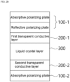
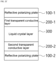
- the first transparent conductive layer 200-1 and the second transparent conductive layer 200-2 may be respectively formed by directly contacting with the first polarizing plate 100-1 and the second polarizing plate 100-2.
- an optical stack used to manufacture a smart window, etc. is manufactured by forming a conductive layer for driving a liquid crystal on one surface of a substance and bonding-coupling a second surface of the substrate to a polarizing plate.
- the variable transmittance optical stack has the conductive layer directly formed on one surface of the polarizing plate without a separate or additional substance for forming the conductive layer, and thus is characterized to improve the transmittance in the light transmissive mode and the curvature characteristic while reducing the entire thickness of the laminate.
- the transparent conductive layer 200 may be formed by being directly deposited on one surface of the polarizing plate 100.
- the transparent conductive layer 200 may be formed by performing pre-processing such as a corona processing or a plasma processing on one surface of each polarizing plate 100, and then directly contacting with the surface of each polarizing plate 100 to which the pre-processing is performed.
- the pre-processing is not limited to the corona processing or the plasma processing, and may adopt a pre-processing currently developed or to be developed without harming the purpose of the present disclosure.
- the transparent conductive layer 200 may be formed by directly contacting with each polarizing plate with the highly adhesive layer (not shown) located therebetween, the highly adhesive layer being provided on one surface of each polarizing plate 100.
- the transparent conductive layer 200 is preferably have the transmittance with respect to visible light of 50% or more, and for example, may include one or more types selected from a group consisting of transparent conductive oxide, metal, carbonaceous material, conductive polymer, conductive ink, and nanowires, but the present disclosure is not limited thereto, and a material of a transparent conductive layer currently developed or to be developed may be used.
- the metal may include one or more types selected from a group consisting of aurum (Au), argentum (Ag), cuprum (Cu), aluminum (Al), platinum (Pt), palladium (Pd), chromium (Cr), titanium (Ti), tungsten (W), niobium (Nb), tantalum (Ta), vanadium (V), iron (Fe), manganese (Mn), cobalt (Co), nickel (Ni), zinc (Zn), alloy containing at least one of them, etc., and for example, may include argentum - palladium - cuprum (APC) alloy or cuprum - calcium (CuCa) alloy.
- the carbonaceous material may include one or more types selected from a group consisting of carbon nanotube (CNT), graphene, etc.
- the conductive polymer may include one or more types selected from a group consisting of polypyrrole, polythiophene, polyacetylene, PEDOT, polyaniline, etc.
- the conductive ink may be a mixture of metal powder and curable polymer binder, and the nanowires may be for example silver nanowires (AgNW).
- the transparent conductive layer 200 may be formed by combining these matters in a structure of two or more layers.
- the transparent conductive layer may be formed in a structure of two layers including a metal layer and a transparent conductive oxide.
- the transparent conductive layer 200 may be formed in a method commonly used in the art and, for example, may be formed using a coating process such as a spin coating method, a roller coating method, a bar coating method, a dip coating method, Gravure coating method, a curtain coating method, a dye coating method, a spray coating method, a doctor coating method, a kneader coating method, etc.; a printing process such as a screen printing method, a spray printing method, an inkjet printing method, a letterpress method, an intaglio printing method, a lithography method, etc.; and a deposition process such as chemical vapor deposition (CVD), physical vapor deposition (PVD), plasma enhanced chemical vapor deposition (PECVD), etc.
- a coating process such as a spin coating method, a roller coating method, a bar coating method, a dip coating method, Gravure coating method, a curtain coating method, a dye coating method, a spray coating method, a doctor coating method, a
- the liquid crystal layer 300 may adjust transmittance of light incident in one or a plurality of directions according to electric fields to change a driving mode of the optical stack.
- the liquid crystal layer 300 may include liquid crystal compounds and, for example, in an optical control region, may be located in a space provided by a sealant layer (not shown) and a spacer (not shown) that are provided between the first polarizing plate 100-1 and the second polarizing plate 100-2.
- the liquid crystal compounds are driven in response to electric fields and is not particularly limited as long as it can control transmittance of light, and liquid crystal compounds currently developed or to be developed may be used and, for example, the description of reactive liquid crystal compound of the above-mentioned coated polarizer may be equally applied thereto.
- the liquid crystal layer 300 may be driven in a twisted nematic (TN) mode.
- optical design with the polarizing plate 100 described above may improve the variable transmittance range between the light transmissive mode and the light blocking mode of the optical stack, and enlargement of the optical stack may be efficiently performed, which is an advantage.
- the sealant may include curable resins as base resins.
- base resins UV curable resins or heat curable resins that are known to be usable for sealants in the art may be used.
- the ultraviolet curable resins may be polymers of UV curable monomers.
- the heat curable resins may be polymers of heat curable monomers.
- the base resins of the sealant for example, acrylate-based resins, epoxy-based resins, urethane-based resins, phenol-based resins, or compounds of these resins.
- the base resins may be acrylate-based resins, and the acrylate-based resins may be polymers of acrylic monomers.
- the acrylic monomers may be multifunctional acrylate.
- the sealant may include monomer substances in addition to the base resins.
- the monomer substances may be monofunctional acrylate.
- the monofunctional acrylate may mean compounds having one acryl group
- the multifunctional acrylate may mean compounds having two or more acryl group.
- the curable resins may be cured by UV irradiation and/or heating.
- the UV irradiation condition or heat condition may be performed appropriately within the scope that does not damage the objective of the present disclosure.
- the sealant may include initiators, for example, optical initiators or heat initiators.
- the sealant may be provided in a method commonly used in the art and, for example, may be formed drawing a sealant at an outer portion of the liquid crystal layer (i.e., inactivate region) with a dispenser having a nozzle.
- the spacer may include at least one spacer among a ball spacer and a column spacer, and specifically, may preferably be a ball spacer.
- the ball spacer may include one or more ball spaces, and preferably has a diameter between 1 and 10 ⁇ m. Furthermore, when viewed in a planar direction, a region where the ball spacer is occupied in the liquid crystal layer 300 is preferably 0.01 to10% of the area of the liquid crystal layer 300 in an aspect of improvement of user's visibility and transmittance in a light transmissive mode.
- the liquid crystal layer 300 may include an alignment film 400 if necessary (referring to FIG. 3A ) and, alignment films 400, for example, may be formed on opposite surfaces of the liquid crystal layer 300 including liquid crystal compounds.
- the alignment film 400 is not particularly limited as long as it adds the orientation to the liquid crystal compounds.
- the alignment film 400 may be manufactured by coating and hardening an alignment film coating composition containing aligned polymers, photopolymerization initiators, and solvent.
- the aligned polymer is not particularly limited, the aligned polymer may be polyacrylate-based resin, polyamic resin, polyimide-based resin, polymer having cinnamate groups, etc. and may use polymer capable of expressing orientation, the polymer being currently developed or to be developed.
- variable transmittance optical stack of the present disclosure may include other members without affecting the objectives of the present disclosure and, for example, may include the pressure sensitive adhesive/adhesive layer 500 (referring to 3B) and may include an ultraviolet ray absorption layer, a hard coating layer, etc.
- the pressure sensitive adhesive/adhesive layer 500 may be formed using an adhesive or a pressure sensitive adhesive, and have appropriate pressure sensitive adhesion/adhesion to prevent peeling, bubbles, etc. from occurring when handling the optical stack, and preferably have transparency and thermal stability.
- the adhesive may adopt an adhesive currently developed or to be developed, for example, may use photocurable adhesive.
- the reactive oligomers are important components that determine the properties of adhesive, and form polymer binding by photopolymerization to form a cured film.
- the available oligomers may be polyester-based resin, polyether-based resin, polyurethane-based resin, epoxy-based resin, polyacryl-based resin, silicon-based resin, and the like.
- the reactive monomers may serve as crosslinker, diluent of the reactive oligomers described above, and affect adhesion characteristics.
- the available reactive monomers may be monofunctional monomers, multifunctional monomers, epoxy-based monomers, vinyl ethers, cyclic ethers, and the like.
- the photopolymerization initiator may absorb light energy to generate radicals or cations to initiate photopolymerization, and a proper kind may be selected and used depending on photopolymerization resin.
- the pressure sensitive adhesive may use a pressure sensitive adhesive currently developed or to be developed.
- a pressure sensitive adhesive acrylic-based pressure sensitive adhesive, rubber-based pressure sensitive adhesive, silicon-based pressure sensitive adhesive, urethane-based pressure sensitive adhesive, polyvinyl alcohol-based pressure sensitive adhesive, polyvinyl pyrrolidone-based pressure sensitive adhesive, polyacrylamide-based pressure sensitive adhesive, cellulose-based pressure sensitive adhesive, vinylalky ether-based pressure sensitive adhesive and the like.
- the pressure sensitive adhesive is not particularly limited as long as it has pressure sensitive adhesion and viscoelasticity.
- the pressure sensitive adhesive may include acrylic-based pressure sensitive adhesive, for example, may be (meth) acrylate copolymers, crosslinkers, solvents, and the like.
- the crosslinkers may adopt crosslinkers currently developed or to be developed and, for example, polyisocyanate compounds, epoxy resins, melamine resins, urea resins, dialdehydes, methylol polymers, etc., and may preferably include polyisocyanate compounds.
- the thickness of the pressure sensitive adhesive/adhesive layer 500 may be appropriately determined depending on a kind of resins serving as the pressure sensitive adhesive/adhesive, the strength of the pressure sensitive adhesive/adhesive, the environment where the pressure sensitive adhesive/adhesive is used, and the like.
- the pressure sensitive adhesive/adhesive layer may have a thickness between 0.01 and 50 ⁇ m in order to ensure sufficient adhesion and minimize the thickness of the optical stack and, preferably, may have a thickness between 0.05 and 20 ⁇ m and, more preferably, may have a thickness between 0.1 and 10 ⁇ m.
- the ultraviolet ray absorption layer is not particularly limited as long as it is to prevent deterioration of the optical stack due to UV rays.
- the ultraviolet ray absorption layer may use salicylic acid-based ultraviolet absorber (phenyl salicylate, p-tert-butylsalicylate, etc.), benzophenone-based ultraviolet absorber(2,4-dihydroxybenzophenone, 2,2'-dihydroxy-4,4'-dimethoxybenzophenone, etc.), benzotriazole-based ultraviolet absorber (2-(2'-hydroxy-5'-methylphenyl)benzotriazole, 2-(2'-hydroxy-3',5'-di-tert-butylphenyl)benzotriazole, 2-(2'-hydroxy-3'-tert-butyl-5'-methylphenyl)benzotriazole, 2-(2'-hydroxy-3',5'-di-tert-butylphenyl)-5-chlorobenzotriazole, 2-(2'
- the present disclosure includes a smart window including the same. Furthermore, the present disclosure includes a vehicle in which the smart window is applied to at least one of front windows, rear windows, side windows, sunroof windows, and inner partitions, and a building window including the smart window.
- An absorptive polarizing plate (outdoor side polarizing plate) is manufactured by bonding a cellulose triacetate film (25 ⁇ m TAC, manufactured by Konica) and a cyclo-olefin film (23 ⁇ m COP, manufactured by Zeon) on opposite surfaces of a polyvinyl alcohol-based polarizer (12 ⁇ m) with an adhesive. Thereafter, a transparent conductive layer is formed by sputtering ITO on a surface of the cyclo-olefin film of the absorptive polarizing plate.
- a reflective polarizing plate is manufactured by bonding a reflective polarizer (APF, manufactured by 3M) on one surface of a cyclo-olefin film (23 ⁇ m COP, manufactured by Zeon), and then the indoor-side polarizing plate is manufactured by bonding the reflective polarizing plate and the second absorptive polarizing plate with an adhesive formed on the cyclo-olefin film of the second absorptive polarizing plate.
- APF reflective polarizer
- 3M cyclo-olefin film
- Each of a first reflective polarizing plate (outdoor side polarizing plate) and a second reflective polarizing plate (indoor side polarizing plate) may be manufactured by bonding a reflective polarizer (APF, manufactured by 3M) on one surface of a cyclo-olefin film (23 ⁇ m COP, manufactured by Zeon). Thereafter, a transparent conductive layer is formed by sputtering ITO on a surface of the cyclo-olefin film of each of the first reflective polarizing plate and the second reflective polarizing plate.
- APF reflective polarizer
- a transparent conductive layer is formed by sputtering ITO on a surface of the cyclo-olefin film of each of the first reflective polarizing plate and the second reflective polarizing plate.
- an optical stack in the example 3 is manufactured by forming an alignment film on the transparent conductive layer of each of the first and second reflective polarizing plate and then bonding the films with a liquid crystal layer, which is driven in the TN mode, located therebetween.
- a transmission axis of the first reflective polarizing plate and a transmission axis of the second reflective polarizing plate are perpendicular to each other.
- the optical stack in the comparative example 1 is manufactured by respectively forming alignment films on the transparent conductive layer of the first absorptive polarizing plate and the transparent conductive layer of the second absorptive polarizing plate, and then being bonded together with the liquid crystal, which is driven in the TN mode, located therebetween.
- a transmission axis of the first absorptive polarizing plate and a transmission axis of the second absorptive polarizing plate are perpendicular to each other.
- each of the variable transmittance optical stacks in the examples 1 to 3 including at least one reflective polarizing plate has a variable transmittance range ranged from 35.7 % to 40.5 %.
Landscapes
- Physics & Mathematics (AREA)
- Nonlinear Science (AREA)
- Optics & Photonics (AREA)
- General Physics & Mathematics (AREA)
- Chemical & Material Sciences (AREA)
- Crystallography & Structural Chemistry (AREA)
- Mathematical Physics (AREA)
- Engineering & Computer Science (AREA)
- Structural Engineering (AREA)
- Mechanical Engineering (AREA)
- Civil Engineering (AREA)
- Architecture (AREA)
- Polarising Elements (AREA)
- Spectroscopy & Molecular Physics (AREA)
- Laminated Bodies (AREA)
Applications Claiming Priority (2)
| Application Number | Priority Date | Filing Date | Title |
|---|---|---|---|
| KR1020210111496A KR102950099B1 (ko) | 2021-08-24 | 2021-08-24 | 광학 적층체 및 이의 제조방법과, 이를 포함하는 스마트 윈도우 및 이를 적용한 자동차 또는 건물용 창호 |
| PCT/KR2022/011952 WO2023027390A1 (ko) | 2021-08-24 | 2022-08-10 | 광학 적층체 및 이의 제조방법과, 이를 포함하는 스마트 윈도우, 이를 적용한 자동차 및 건물용 창호 |
Publications (2)
| Publication Number | Publication Date |
|---|---|
| EP4394494A1 true EP4394494A1 (de) | 2024-07-03 |
| EP4394494A4 EP4394494A4 (de) | 2024-12-25 |
Family
ID=85323281
Family Applications (1)
| Application Number | Title | Priority Date | Filing Date |
|---|---|---|---|
| EP22861600.9A Withdrawn EP4394494A4 (de) | 2021-08-24 | 2022-08-10 | Optisches laminat und herstellungsverfahren dafür, intelligentes fenster damit sowie fahrzeug und gebäudefenster oder -tür damit |
Country Status (4)
| Country | Link |
|---|---|
| US (1) | US20240248343A1 (de) |
| EP (1) | EP4394494A4 (de) |
| KR (1) | KR102950099B1 (de) |
| WO (1) | WO2023027390A1 (de) |
Cited By (1)
| Publication number | Priority date | Publication date | Assignee | Title |
|---|---|---|---|---|
| EP4603900A1 (de) * | 2023-11-15 | 2025-08-20 | Dongwoo Fine-Chem Co., Ltd. | Optischer stapel mit variabler durchlässigkeit |
Family Cites Families (16)
| Publication number | Priority date | Publication date | Assignee | Title |
|---|---|---|---|---|
| GB9223741D0 (en) * | 1992-11-12 | 1992-12-23 | Crystalens Ltd | Liquid crystal device |
| KR100432457B1 (ko) * | 1993-12-21 | 2004-05-22 | 미네소타 마이닝 앤드 매뉴팩춰링 캄파니 | 휘도 향상 디바이스 |
| GB9806313D0 (en) * | 1997-06-28 | 1998-05-20 | Sharp Kk | Method of making a spatial light modulator method of making a cell wall for a spatial light modulator spatial light modulator and cell wall for such aspatial |
| US7525604B2 (en) * | 2005-03-15 | 2009-04-28 | Naxellent, Llc | Windows with electrically controllable transmission and reflection |
| KR101482625B1 (ko) * | 2008-06-24 | 2015-01-14 | 삼성디스플레이 주식회사 | 투과 및 반사 전환형 디스플레이 장치 |
| KR20130110915A (ko) * | 2012-03-30 | 2013-10-10 | 삼성디스플레이 주식회사 | 액정 표시 장치 |
| KR101706820B1 (ko) * | 2014-07-03 | 2017-02-14 | 삼성에스디아이 주식회사 | 액정표시장치용 모듈 및 이를 포함하는 액정표시장치 |
| KR102431690B1 (ko) * | 2015-11-30 | 2022-08-11 | 엘지디스플레이 주식회사 | 스마트 액정표시장치 |
| US10247996B2 (en) * | 2016-06-22 | 2019-04-02 | Gentex Corporation | Thermal control of variable transmittance windows |
| JP6128270B1 (ja) | 2016-07-11 | 2017-05-17 | 大日本印刷株式会社 | 調光フィルム |
| KR102136102B1 (ko) * | 2017-04-25 | 2020-07-22 | 주식회사 엘지화학 | 광학 디바이스 |
| JP2019095597A (ja) | 2017-11-22 | 2019-06-20 | スタンレー電気株式会社 | 液晶装置 |
| KR102184392B1 (ko) * | 2017-11-28 | 2020-11-30 | 주식회사 엘지화학 | 광학 디바이스 |
| KR101999352B1 (ko) * | 2017-12-15 | 2019-07-11 | 성문전자주식회사 | 투과율이 가변되는 스마트 윈도우용 변색필름 |
| KR101920854B1 (ko) * | 2018-01-05 | 2018-11-21 | 주식회사 엔디스 | 차량용 스마트 윈도우 |
| KR102183706B1 (ko) * | 2018-08-14 | 2020-11-27 | 주식회사 엘지화학 | 광학 디바이스 |
-
2021
- 2021-08-24 KR KR1020210111496A patent/KR102950099B1/ko active Active
-
2022
- 2022-08-10 WO PCT/KR2022/011952 patent/WO2023027390A1/ko not_active Ceased
- 2022-08-10 US US18/293,036 patent/US20240248343A1/en not_active Abandoned
- 2022-08-10 EP EP22861600.9A patent/EP4394494A4/de not_active Withdrawn
Cited By (1)
| Publication number | Priority date | Publication date | Assignee | Title |
|---|---|---|---|---|
| EP4603900A1 (de) * | 2023-11-15 | 2025-08-20 | Dongwoo Fine-Chem Co., Ltd. | Optischer stapel mit variabler durchlässigkeit |
Also Published As
| Publication number | Publication date |
|---|---|
| KR102950099B1 (ko) | 2026-04-09 |
| WO2023027390A1 (ko) | 2023-03-02 |
| EP4394494A4 (de) | 2024-12-25 |
| KR20230029240A (ko) | 2023-03-03 |
| US20240248343A1 (en) | 2024-07-25 |
Similar Documents
| Publication | Publication Date | Title |
|---|---|---|
| EP4350427A1 (de) | Optisches laminat und herstellungsverfahren dafür, intelligentes fenster damit sowie fenster und tür für fahrzeug oder gebäude damit | |
| EP4350429A1 (de) | Optisches laminat, verfahren zur herstellung davon, intelligentes fenster damit und fenster für fahrzeug oder gebäude damit | |
| EP4411470A1 (de) | Optisches laminat und herstellungsverfahren dafür, intelligentes fenster damit sowie tür und fenster für automobil und gebäude damit | |
| EP4372461A1 (de) | Optisches laminat und herstellungsverfahren dafür, intelligentes fenster damit sowie fenster und tür für fahrzeug und gebäude damit | |
| US20240302691A1 (en) | Optical laminate and manufacturing method therefor, smart window comprising same, and window and door for vehicle and building, having same applied thereto | |
| US20240248343A1 (en) | Optical laminate and manufacturing method therefor, smart window comprising same, and vehicle and building window or door employing same | |
| EP4411465A1 (de) | Optisches laminat, verfahren zur herstellung davon, intelligentes fenster damit und fahrzeug und gebäudefenster oder -tür damit | |
| EP4411471A1 (de) | Optisches laminat, verfahren zur herstellung davon, intelligentes fenster damit und fahrzeug und gebäudefenster und -türen damit | |
| KR102763778B1 (ko) | 광학 적층체 및 이의 제조방법과, 이를 포함하는 스마트 윈도우 및 이를 적용한 자동차 또는 건물용 창호 | |
| KR102927175B1 (ko) | 광학 적층체 및 이의 제조방법과, 이를 포함하는 스마트 윈도우 및 이를 적용한 자동차 또는 건물용 창호 | |
| EP4468073A1 (de) | Optischer stapel, verfahren zur herstellung davon und intelligentes fenster damit | |
| EP4424506A1 (de) | Optisches laminat und herstellungsverfahren dafür, intelligentes fenster damit sowie tür und fenster für automobil und gebäude damit | |
| EP4459365A1 (de) | Optisches laminat und herstellungsverfahren dafür, intelligentes fenster damit sowie automobil- und gebäudefenstersysteme damit | |
| EP4451048A1 (de) | Flüssigkristallverpackung und herstellungsverfahren dafür, optischer stapel damit und intelligentes fenster damit | |
| KR102740412B1 (ko) | 투과율 가변 광학 적층체 및 이를 포함하는 스마트 윈도우 | |
| EP4560392A1 (de) | Optischer stapel und herstellungsverfahren dafür, intelligentes fenster damit und automobil oder fenster für gebäude damit | |
| EP4425247A1 (de) | Optischer stapel und herstellungsverfahren dafür sowie intelligentes fenster damit und automobil oder fenster für gebäude damit | |
| EP4560390A1 (de) | Optischer stapel und herstellungsverfahren dafür, intelligentes fenster damit und automobil oder fenster für gebäude damit | |
| KR20240130213A (ko) | 광학 적층체 및 이의 제조방법과, 이를 포함하는 스마트 윈도우 및 이를 적용한 자동차 또는 건물용 창호 |
Legal Events
| Date | Code | Title | Description |
|---|---|---|---|
| STAA | Information on the status of an ep patent application or granted ep patent |
Free format text: STATUS: THE INTERNATIONAL PUBLICATION HAS BEEN MADE |
|
| PUAI | Public reference made under article 153(3) epc to a published international application that has entered the european phase |
Free format text: ORIGINAL CODE: 0009012 |
|
| STAA | Information on the status of an ep patent application or granted ep patent |
Free format text: STATUS: REQUEST FOR EXAMINATION WAS MADE |
|
| 17P | Request for examination filed |
Effective date: 20240325 |
|
| AK | Designated contracting states |
Kind code of ref document: A1 Designated state(s): AL AT BE BG CH CY CZ DE DK EE ES FI FR GB GR HR HU IE IS IT LI LT LU LV MC MK MT NL NO PL PT RO RS SE SI SK SM TR |
|
| REG | Reference to a national code |
Ref country code: DE Ref legal event code: R079 Free format text: PREVIOUS MAIN CLASS: G02F0001137000 Ipc: E06B0009240000 |
|
| DAV | Request for validation of the european patent (deleted) | ||
| DAX | Request for extension of the european patent (deleted) | ||
| A4 | Supplementary search report drawn up and despatched |
Effective date: 20241125 |
|
| RIC1 | Information provided on ipc code assigned before grant |
Ipc: G02B 5/30 20060101ALI20241119BHEP Ipc: G02F 1/1343 20060101ALI20241119BHEP Ipc: G02F 1/1335 20060101ALI20241119BHEP Ipc: E06B 9/24 20060101AFI20241119BHEP |
|
| STAA | Information on the status of an ep patent application or granted ep patent |
Free format text: STATUS: EXAMINATION IS IN PROGRESS |
|
| 17Q | First examination report despatched |
Effective date: 20251212 |
|
| STAA | Information on the status of an ep patent application or granted ep patent |
Free format text: STATUS: THE APPLICATION HAS BEEN WITHDRAWN |
|
| 18W | Application withdrawn |
Effective date: 20260327 |