EP4394512A1 - Quellenmaskenoptimierung auf der basis systematischer effekte auf einen lithographischen apparat - Google Patents
Quellenmaskenoptimierung auf der basis systematischer effekte auf einen lithographischen apparat Download PDFInfo
- Publication number
- EP4394512A1 EP4394512A1 EP22216705.8A EP22216705A EP4394512A1 EP 4394512 A1 EP4394512 A1 EP 4394512A1 EP 22216705 A EP22216705 A EP 22216705A EP 4394512 A1 EP4394512 A1 EP 4394512A1
- Authority
- EP
- European Patent Office
- Prior art keywords
- layer
- lithographic apparatus
- source
- features
- source configuration
- Prior art date
- Legal status (The legal status is an assumption and is not a legal conclusion. Google has not performed a legal analysis and makes no representation as to the accuracy of the status listed.)
- Withdrawn
Links
Images





Classifications
-
- G—PHYSICS
- G03—PHOTOGRAPHY; CINEMATOGRAPHY; ANALOGOUS TECHNIQUES USING WAVES OTHER THAN OPTICAL WAVES; ELECTROGRAPHY; HOLOGRAPHY
- G03F—PHOTOMECHANICAL PRODUCTION OF TEXTURED OR PATTERNED SURFACES, e.g. FOR PRINTING, FOR PROCESSING OF SEMICONDUCTOR DEVICES; MATERIALS THEREFOR; ORIGINALS THEREFOR; APPARATUS SPECIALLY ADAPTED THEREFOR
- G03F7/00—Photomechanical, e.g. photolithographic, production of textured or patterned surfaces, e.g. printing surfaces; Materials therefor, e.g. comprising photoresists; Apparatus specially adapted therefor
- G03F7/70—Microphotolithographic exposure; Apparatus therefor
- G03F7/70058—Mask illumination systems
- G03F7/70125—Use of illumination settings tailored to particular mask patterns
-
- G—PHYSICS
- G03—PHOTOGRAPHY; CINEMATOGRAPHY; ANALOGOUS TECHNIQUES USING WAVES OTHER THAN OPTICAL WAVES; ELECTROGRAPHY; HOLOGRAPHY
- G03F—PHOTOMECHANICAL PRODUCTION OF TEXTURED OR PATTERNED SURFACES, e.g. FOR PRINTING, FOR PROCESSING OF SEMICONDUCTOR DEVICES; MATERIALS THEREFOR; ORIGINALS THEREFOR; APPARATUS SPECIALLY ADAPTED THEREFOR
- G03F7/00—Photomechanical, e.g. photolithographic, production of textured or patterned surfaces, e.g. printing surfaces; Materials therefor, e.g. comprising photoresists; Apparatus specially adapted therefor
- G03F7/70—Microphotolithographic exposure; Apparatus therefor
- G03F7/70425—Imaging strategies, e.g. for increasing throughput or resolution, printing product fields larger than the image field or compensating lithography- or non-lithography errors, e.g. proximity correction, mix-and-match, stitching or double patterning
- G03F7/70433—Layout for increasing efficiency or for compensating imaging errors, e.g. layout of exposure fields for reducing focus errors; Use of mask features for increasing efficiency or for compensating imaging errors
- G03F7/70441—Optical proximity correction [OPC]
-
- G—PHYSICS
- G03—PHOTOGRAPHY; CINEMATOGRAPHY; ANALOGOUS TECHNIQUES USING WAVES OTHER THAN OPTICAL WAVES; ELECTROGRAPHY; HOLOGRAPHY
- G03F—PHOTOMECHANICAL PRODUCTION OF TEXTURED OR PATTERNED SURFACES, e.g. FOR PRINTING, FOR PROCESSING OF SEMICONDUCTOR DEVICES; MATERIALS THEREFOR; ORIGINALS THEREFOR; APPARATUS SPECIALLY ADAPTED THEREFOR
- G03F7/00—Photomechanical, e.g. photolithographic, production of textured or patterned surfaces, e.g. printing surfaces; Materials therefor, e.g. comprising photoresists; Apparatus specially adapted therefor
- G03F7/70—Microphotolithographic exposure; Apparatus therefor
- G03F7/70483—Information management; Active and passive control; Testing; Wafer monitoring, e.g. pattern monitoring
- G03F7/70491—Information management, e.g. software; Active and passive control, e.g. details of controlling exposure processes or exposure tool monitoring processes
- G03F7/705—Modelling or simulating from physical phenomena up to complete wafer processes or whole workflow in wafer productions
-
- G—PHYSICS
- G03—PHOTOGRAPHY; CINEMATOGRAPHY; ANALOGOUS TECHNIQUES USING WAVES OTHER THAN OPTICAL WAVES; ELECTROGRAPHY; HOLOGRAPHY
- G03F—PHOTOMECHANICAL PRODUCTION OF TEXTURED OR PATTERNED SURFACES, e.g. FOR PRINTING, FOR PROCESSING OF SEMICONDUCTOR DEVICES; MATERIALS THEREFOR; ORIGINALS THEREFOR; APPARATUS SPECIALLY ADAPTED THEREFOR
- G03F7/00—Photomechanical, e.g. photolithographic, production of textured or patterned surfaces, e.g. printing surfaces; Materials therefor, e.g. comprising photoresists; Apparatus specially adapted therefor
- G03F7/70—Microphotolithographic exposure; Apparatus therefor
- G03F7/708—Construction of apparatus, e.g. environment aspects, hygiene aspects or materials
- G03F7/70858—Environment aspects, e.g. pressure of beam-path gas, temperature
- G03F7/70883—Environment aspects, e.g. pressure of beam-path gas, temperature of optical system
- G03F7/70891—Temperature
Definitions
- the present disclosure relates to source mask optimization based on systematic effects on a lithographic apparatus.
- a lithographic apparatus is a machine constructed to apply a desired pattern onto a substrate.
- a lithographic apparatus can be used, for example, in the manufacture of integrated circuits (ICs).
- a lithographic apparatus may, for example, project a pattern (also often referred to as "design layout" or "design") at a patterning device (e.g., a mask) onto a layer of radiation-sensitive material (resist) provided on a substrate (e.g., a wafer).
- a lithographic apparatus may use electromagnetic radiation.
- the wavelength of this radiation determines the minimum size of features which can be formed on the substrate. Typical wavelengths currently in use are 365 nm (i-line), 248 nm, 193 nm and 13.5 nm.
- a lithographic apparatus which uses extreme ultraviolet (EUV) radiation, having a wavelength within the range 4-20 nm, for example 6.7 nm or 13.5 nm, may be used to form smaller features on a substrate than a lithographic apparatus which uses, for example, radiation with a wavelength of 193 nm.
- EUV extreme ultraviolet
- Low-k1 lithography may be used to process features with dimensions smaller than the classical resolution limit of a lithographic apparatus.
- the smaller k1 the more difficult it becomes to reproduce the pattern on the substrate that resembles the shape and dimensions planned by a circuit designer in order to achieve particular electrical functionality and performance.
- sophisticated fine-tuning steps may be applied to the lithographic projection apparatus and/or design layout.
- RET resolution enhancement techniques
- a first layer's source configuration e.g., illumination pupil
- mirror heating based SMO may be performed to generate a prior (first) (e.g., metal) layer illumination pupil with mitigated mirror heating impact to a subsequent (second) (e.g., via) layer patterning.
- mirror heating based SMO may be performed to generate a second (e.g., via) layer illumination pupil with reduced sensitivity to mirror heating induced aberration caused by prior metal layer exposure(s).
- the layers in this example may be reversed such that the via layer is the first layer and the metal layer is the second layer, the first and second layers may both be metal or both be via layers, the layers may be associated with different wafers in different production lots, and/or other configurations are possible.
- a method for source optimization or source mask optimization for a lithographic apparatus comprises components configured to image a pattern onto a substrate.
- the method comprises determining a source configuration of the lithographic apparatus for first features in a first layer of the pattern based on systematic effects on the lithographic apparatus components that cause feature dependent imaging performance changes for second features in a second layer, where the second and the first layers can be of the same pattern or different patterns.
- the first layer is processed (e.g., exposed) on the lithographic apparatus before the second layer, for example.
- the first layer is to be processed immediately before the second layer.
- the first layer is to be processed before another layer and then the second layer.
- a model e.g., a mirror heating model
- determining a source configuration comprises determining an illumination pupil and/or other operations.
- the lithographic apparatus components comprise a mirror, a lens, and/or a full optical system (e.g., that includes one or more mirrors, one or more lenses, and/or or several other components), and the systematic effects on the lithographic apparatus comprise mirror and/or lens heating.
- the systematic effects on the lithographic apparatus components vary over time during exposure and/or over multiple exposures.
- feature dependent imaging performance changes comprise changes that vary based on a shape, location, dimensions, material, layer, and/or function of a feature in a layer of the pattern.
- the method comprises determining a second source configuration for the second features in the second layer of the pattern based on a second feature sensitivity to the systematic effects , wherein the systematic effect is associated with processing the first features of the first layer.
- the first layer is to be processed before the second layer.
- the sensitivity corresponds to sensitivity of imaging performance to heating effect.
- the sensitivity corresponds to aberration (Zernike or Tatian) sensitivity of important cutline metrics, including EPE, CD, and PPE sensitivities. The sensitivity indicates how severe the metric is impacted by the aberration wavefront.
- the source configuration for processing the second layer is determined based on systematic effects on the lithographic apparatus components that is caused by processing the first features in the first layer.
- the sensitivity is determined by simulation based on one or more prior exposures for one or more prior patterning operations.
- a mirror heating model is used to predict the heating effect resulting from processing the first layer, and the model output (e.g., resultant wavefront or aberration) is used in a source optimization process to generate a source configuration for processing the second layer.
- the source optimization process uses a cost function including indication of second layer's sensitivity to mirror heating induced aberration.
- the first features can be produced using a first mask comprising a first portion of a pattern design layout
- the second features are produced with a second mask comprising a second portion of the same pattern design layout, or a different pattern design layout.
- determining the source configuration comprises performing source mask optimization on the source configuration for the first features in the first layer with a cost function indicating imaging performance of the second features in the second layer.
- the two layers may belong to the same pattern or different patterns, the same design layout or different design layout, and/or the same or different products (e.g., wafers).
- the first layer is a metal layer and the second layer is a via layer.
- the first (e.g., metal) layer is exposed before the second (e.g., via) layer, and heating from exposing the first layer is accounted for when determining the source configuration of the lithographic apparatus for features (e.g., vias) in the second layer.
- the lithographic apparatus components comprise an illumination source and projection optics configured to image the pattern onto the substrate.
- the method comprises determining one or more adjustments for one or more of the source configuration, the pattern, the projection optics, or the illumination source based on the systematic effects on the lithographic apparatus components that cause the feature dependent imaging performance changes until a termination condition is satisfied.
- the termination condition comprises a determination that features patterned onto the substrate will substantially match a target design.
- the method comprises mask co-optimization with the source configuration for the first features in the first layer of the pattern based on the systematic effects on the lithographic apparatus components that cause the imaging performance changes for the second features in the second layer of the pattern.
- a system comprising one or more processors configured by machine readable instructions to perform one or more of the operations of the method described above.
- Source optimization (SO) or SMO for a lithographic apparatus to reduce systematic impact in lithography process comprises determining a source configuration (e.g., determining an illumination pupil) of the lithographic apparatus for first features in a first layer of a pattern based on systematic effect impact on imaging performance of second features in a second layer that is processed later than the first layer.
- a source configuration e.g., determining an illumination pupil
- the present disclosure can be used to address other systematic effects, such as component heating, component cooling, component drift, component variation for different substrate lots, illumination offsets, mask to mask changes, overlay effects, aberration effects, fading, re-calibration or re-setup, and/or dose or pupil residuals, etc.
- Layers of a pattern may refer to different layers of the same pattern for one product, a first layer for one product and a second layer for a different product, etc. (e.g., not necessarily simply an order of layers in a single stack).
- mirror heating associated with a current layer can affect a second patterned (e.g., via) layer exposure.
- first (e.g., metal) layer can affect a second patterned (e.g., via) layer exposure.
- mirror heating based SMO may be performed to generate a metal layer illumination pupil that creates less mirror heating impact to a subsequent via layer exposure, and/or mirror heating based SMO may be performed to generate a via layer illumination pupil that is less sensitive to mirror heating caused by prior metal layer exposure.
- a "printed pattern" means the physical pattern on a substrate that was etched based on a target pattern.
- the printed pattern can include, for example, troughs, channels, depressions, edges, or other two and three dimensional features resulting from a lithography process.
- FIG. 1 is a schematic diagram of a lithographic projection apparatus LA, according to an embodiment.
- the lithographic projection apparatus LA includes an illumination system (also referred to as illuminator) IL configured to condition a radiation beam B (e.g., UV radiation, DUV radiation or EUV radiation), a mask support (e.g., a mask table) MT constructed to support a patterning device (e.g., a mask) MA and connected to a first positioner PM configured to accurately position the patterning device MA in accordance with certain parameters, a substrate support (e.g., a wafer table) WT constructed to hold a substrate (e.g., a resist coated wafer) W and connected to a second positioner PW configured to accurately position the substrate support in accordance with certain parameters, and a projection system (e.g., a refractive projection lens system) PS configured to project a pattern imparted to the radiation beam B by patterning device MA onto a target portion C (e.g., comprising one or
- the illumination system IL receives a radiation beam from a radiation source SO, e.g. via a beam delivery system BD.
- the illumination system IL may include various types of optical components, such as refractive, reflective, magnetic, electromagnetic, electrostatic, and/or other types of optical components, or any combination thereof, for directing, shaping, and/or controlling radiation.
- the illuminator IL may be used to condition the radiation beam B to have a desired spatial and angular intensity distribution in its cross section at a plane of the patterning device MA.
- projection system PS used herein should be broadly interpreted as encompassing various types of projection system, including refractive, reflective, catadioptric, anamorphic, magnetic, electromagnetic and/or electrostatic optical systems, or any combination thereof, as appropriate for the exposure radiation being used, and/or for other factors such as the use of an immersion liquid or the use of a vacuum. Any use of the term “projection lens” herein may be considered as synonymous with the more general term “projection system” PS.
- the lithographic apparatus LA may comprise a measurement stage.
- the measurement stage is arranged to hold a sensor and/or a cleaning device.
- the sensor may be arranged to measure a property of the projection system PS or a property of the radiation beam B.
- the measurement stage may hold multiple sensors.
- the cleaning device may be arranged to clean part of the lithographic apparatus, for example a part of the projection system PS or a part of a system that provides the immersion liquid.
- the measurement stage may move beneath the projection system PS when the substrate support WT is away from the projection system PS.
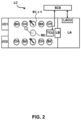
- FIG. 2 depicts a schematic overview of a lithographic cell LC.
- a lithographic projection apparatus shown in Figure 1 and illustrated as lithographic apparatus LA in Figure 2
- lithographic cell LC also sometimes referred to as a lithocell or (litho)cluster, which often also includes apparatus to perform pre- and post-exposure processes on a substrate W ( Figure 1 ).
- these include spin coaters SC configured to deposit resist layers, developers to develop exposed resist, chill plates CH and bake plates BK, e.g., for conditioning the temperature of substrates W, e.g., for conditioning solvents in the resist layers.
- the inspection apparatus may measure the properties using an actual substrate (e.g., a charged particle - SEM - image of a wafer pattern) or an image of an actual substrate, on a latent image (image in a resist layer after the exposure), on a semi-latent image (image in a resist layer after a post-exposure bake step PEB), on a developed resist image (in which the exposed or unexposed parts of the resist have been removed), on an etched image (after a pattern transfer step such as etching), or in other ways.
- an actual substrate e.g., a charged particle - SEM - image of a wafer pattern
- PEB post-exposure bake step
- PEB post-exposure bake step
- a developed resist image in which the exposed or unexposed parts of the resist have been removed
- an etched image after a pattern transfer step such as etching
- metrology tools MT are or include a spectroscopic scatterometer, an ellipsometric scatterometer, or other light based tools.
- a spectroscopic scatterometer may be configured such that the radiation emitted by a radiation source is directed onto target features of a substrate and the reflected or scattered radiation from the target is directed to a spectrometer detector, which measures a spectrum (i.e., a measurement of intensity as a function of wavelength) of the specular reflected radiation. From this data, the structure or profile of the target giving rise to the detected spectrum may be reconstructed, e.g., by rigorous coupled wave analysis and non-linear regression or by comparison with a library of simulated spectra.
- the computational determinations and/or simulations can be used to configure one or more features of the patterning device pattern (e.g., performing optical proximity correction), one or more features of the illumination (e.g., changing one or more characteristics of a spatial / angular intensity distribution of the illumination, such as changing an illumination pupil shape), and/or one or more features of the projection optics (e.g., numerical aperture, etc.).
- This configuration can be generally referred to as, respectively, mask optimization, source optimization, and projection optimization. Optimizations can be performed on their own, or combined in different combinations.
- One example is source-mask optimization (SMO), which involves the configuring of one or more features of the patterning device pattern together with one or more features of the illumination.
- SMO source-mask optimization
- a prior art source mask optimization process is described in United States Patent No. 9,588,438 titled "Optimization Flows of Source, Mask and Projection Optics", which is incorporated in its entirety by reference.
- an optimization process of a system may be represented as a cost function.
- the optimization process may comprise finding a set of parameters (source configurations, design variables, process variables, etc.) of the system that minimizes the cost function.
- the cost function can have any suitable form depending on the goal of the optimization.
- the cost function can be weighted root mean square (RMS) of deviations of certain characteristics (evaluation points) of the system with respect to the intended values (e.g., ideal values) of these characteristics.
- the cost function can also be the maximum of these deviations (i.e., worst deviation).
- evaluation points should be interpreted broadly to include any characteristics of the system, a design, or the fabrication method.
- the design and/or process variables of the system can be confined to finite ranges and/or be interdependent due to practicalities of implementations of the system, design, and/or method.
- the constraints are often associated with physical properties and characteristics of the hardware such as tunable ranges, and/or patterning device manufacturability design rules.
- the evaluation points can include physical points on a resist image on a substrate (e.g., associated with edge placement error and/or other key performance indicators), as well as non-physical characteristics such as dose and focus, for example.
- w p is a weight constant associated with f p ( z 1 , z 2 , ⁇ , z N ).
- the characteristic may be a position of an edge of a pattern, measured at a given point on the edge.
- Different f p ( z 1 , z 2 , ⁇ , z N ) may have different weight w p .
- the weight w p for the f p (z 1 , z 2 , ⁇ , z N ) representing the difference between the actual position and the intended position of the edge may be given a higher value.
- the cost function may represent any one or more suitable characteristics of the lithographic projection apparatus, lithographic process, or the substrate, for instance, a source configuration, a focus, edge placement error (EPE), CD, image shift, image distortion, image rotation, stochastic variation, throughput, local CD variation, process window, an interlayer characteristic, or a combination thereof.
- the cost function may include a function that represents one or more characteristics of the resist image. For example, f p ( z 1 , z 2 , ⁇ , z N ) can be a distance between a point in the resist image to an intended position of that point (i.e., edge placement error EPE p ( z 1 , z 2 , ⁇ , z N ) .
- cost function CF utilizes EPE
- additional weight may be added for CD or PPE, for example, a custom cost function based on CD asymmetry may be applied, and/or other cost functions may be used.
- optimization may be based on any imaging key performance indicator (KPI) that depends on the source and/or pupil being optimized during SMO.
- KPI imaging key performance indicator
- Middle row 730 and bottom row 740 illustrate embodiments of method 600 shown in Figure 6 and described herein.
- Middle row 730 illustrates a metal layer illumination pupil 700 (e.g., a source configuration of a lithographic apparatus for first features in a first layer of a pattern) optimized for (1) metal layer mirror heating and (2) for via layer sensitivity to metal layer mirror heating (e.g., systematic effects on the lithographic apparatus components that cause feature dependent imaging performance changes for second features in a second layer of the pattern).
- metal layer illumination pupil 700 is configured with feature shapes, sizes, and locations that generally accommodate or avoid via layer pupil 710 feature shapes, sizes, and locations (e.g., so as not to cause unnecessary heating).
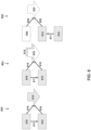
- Figure 8 illustrates an existing systematic effect (e.g., mirror heating) based SMO 800 compared to new systematic effect (e.g., mirror heating) based SMO methods 802 and 804 (e.g., both comprising different example embodiments of method 600) described herein.
- a metal layer illumination pupil 810 causes 811 metal layer mirror heating 812.
- a cost function based on EPE, NILS, and/or other key performance indicators is minimized 814 such that metal layer illumination pupil 810 is optimized for the effects 816 of metal layer mirror heating and for metal layer sensitivity 818 to the metal layer mirror heating.
- metal layer illumination pupil 810 and (e.g., which causes 811) metal layer mirror heating 812 are considered known or fixed.
- a cost function based on via EPE, NILS, and/or other key performance indicators is minimized 820 such that a via layer illumination pupil 850 is optimized for the effects 852 of metal layer mirror heating and/or for via layer sensitivity 854 to the metal layer mirror heating.
- the effect of metal layer mirror heating is equivalent to the sensitivity of via here (because the metal is fixed, not affected here).
- a mirror heating based SMO e.g., SMO 804 input is changed (e.g., the optimization is for via layer illumination pupil 850 instead of metal layer illumination pupil 810).
- SMO 804 is configured such that given heating is less problematic (e.g., there is less overlap with diffraction orders).
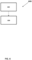
- the lithographic apparatus comprises an illumination source, projection optics, and/or other components configured to image the pattern onto the substrate (as described above related to Figure 1 ).
- performing the source mask optimization comprises modeling a lithographic process for imaging the pattern onto the substrate.
- a model for modeling the process for imaging the pattern onto the substrate uses a determined source configuration (e.g., from operation 602) and/or other information.
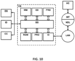
- Computer system CS further includes a read only memory (ROM) ROM or other static storage device coupled to bus BS for storing static information and instructions for processor PRO.
- ROM read only memory
- a storage device SD such as a magnetic disk or optical disk, is provided and coupled to bus BS for storing information and instructions.
- Computer-readable media can be non-transitory, for example, a floppy disk, a flexible disk, hard disk, magnetic tape, any other magnetic medium, a CD-ROM, DVD, any other optical medium, punch cards, paper tape, any other physical medium with patterns of holes, a RAM, a PROM, and EPROM, a FLASH-EPROM, any other memory chip or cartridge.
- Non-transitory computer readable media can have (machine-readable) instructions recorded thereon. The instructions, when executed by a computer, can implement any of the operations described herein.
- Transitory computer-readable media can include a carrier wave or other propagating electromagnetic signal, for example.
- Network link NDL typically provides data communication through one or more networks to other data devices.
- network link NDL may provide a connection through local network LAN to a host computer HC.
- This can include data communication services provided through the worldwide packet data communication network, now commonly referred to as the "Internet" INT.
- Internet may use electrical, electromagnetic, or optical signals that carry digital data streams.
- the signals through the various networks and the signals on network data link NDL and through communication interface CI, which carry the digital data to and from computer system CS, are exemplary forms of carrier waves transporting the information.
- the concepts disclosed herein may be used with any imaging, etching, polishing, inspection, etc. system for sub wavelength features, and may be useful with emerging imaging technologies capable of producing increasingly shorter wavelengths.
- Emerging technologies include EUV (extreme ultra violet), DUV lithography that is capable of producing a 193nm wavelength with the use of an ArF laser, and even a 157nm wavelength with the use of a Fluorine laser.
- EUV lithography is capable of producing wavelengths within a range of 20-50nm by using a synchrotron or by hitting a material (either solid or a plasma) with high energy electrons in order to produce photons within this range.
Landscapes
- Physics & Mathematics (AREA)
- General Physics & Mathematics (AREA)
- Health & Medical Sciences (AREA)
- Life Sciences & Earth Sciences (AREA)
- Atmospheric Sciences (AREA)
- Toxicology (AREA)
- Engineering & Computer Science (AREA)
- Environmental & Geological Engineering (AREA)
- Epidemiology (AREA)
- Public Health (AREA)
- Exposure And Positioning Against Photoresist Photosensitive Materials (AREA)
Priority Applications (4)
| Application Number | Priority Date | Filing Date | Title |
|---|---|---|---|
| EP22216705.8A EP4394512A1 (de) | 2022-12-27 | 2022-12-27 | Quellenmaskenoptimierung auf der basis systematischer effekte auf einen lithographischen apparat |
| PCT/EP2023/085228 WO2024141256A1 (en) | 2022-12-27 | 2023-12-11 | Source mask optimization based on systematic effects on a lithographic apparatus |
| CN202380089061.7A CN120359467A (zh) | 2022-12-27 | 2023-12-11 | 基于光刻设备上的系统效应的源掩模优化 |
| TW112149531A TW202445275A (zh) | 2022-12-27 | 2023-12-19 | 基於微影設備之系統效應之源光罩最佳化 |
Applications Claiming Priority (1)
| Application Number | Priority Date | Filing Date | Title |
|---|---|---|---|
| EP22216705.8A EP4394512A1 (de) | 2022-12-27 | 2022-12-27 | Quellenmaskenoptimierung auf der basis systematischer effekte auf einen lithographischen apparat |
Publications (1)
| Publication Number | Publication Date |
|---|---|
| EP4394512A1 true EP4394512A1 (de) | 2024-07-03 |
Family
ID=84604147
Family Applications (1)
| Application Number | Title | Priority Date | Filing Date |
|---|---|---|---|
| EP22216705.8A Withdrawn EP4394512A1 (de) | 2022-12-27 | 2022-12-27 | Quellenmaskenoptimierung auf der basis systematischer effekte auf einen lithographischen apparat |
Country Status (4)
| Country | Link |
|---|---|
| EP (1) | EP4394512A1 (de) |
| CN (1) | CN120359467A (de) |
| TW (1) | TW202445275A (de) |
| WO (1) | WO2024141256A1 (de) |
Families Citing this family (1)
| Publication number | Priority date | Publication date | Assignee | Title |
|---|---|---|---|---|
| CN120315261B (zh) * | 2025-06-17 | 2025-08-19 | 合肥晶合集成电路股份有限公司 | 一种光学邻近校正模型的建模方法、系统及计算机设备 |
Citations (4)
| Publication number | Priority date | Publication date | Assignee | Title |
|---|---|---|---|---|
| US20130212543A1 (en) * | 2012-02-09 | 2013-08-15 | Asml Netherlands B.V. | Lens heating aware source mask optimization for advanced lithography |
| US20140047397A1 (en) * | 2008-06-03 | 2014-02-13 | Asml Netherlands B.V. | Lens heating compensation systems and methods |
| US9588438B2 (en) | 2010-11-10 | 2017-03-07 | Asml Netherlands B.V. | Optimization flows of source, mask and projection optics |
| US20190137889A1 (en) * | 2016-03-24 | 2019-05-09 | Asml, Netherlands B.V. | Optimization of a lithographic projection apparatus accounting for an interlayer characteristic |
-
2022
- 2022-12-27 EP EP22216705.8A patent/EP4394512A1/de not_active Withdrawn
-
2023
- 2023-12-11 WO PCT/EP2023/085228 patent/WO2024141256A1/en not_active Ceased
- 2023-12-11 CN CN202380089061.7A patent/CN120359467A/zh active Pending
- 2023-12-19 TW TW112149531A patent/TW202445275A/zh unknown
Patent Citations (4)
| Publication number | Priority date | Publication date | Assignee | Title |
|---|---|---|---|---|
| US20140047397A1 (en) * | 2008-06-03 | 2014-02-13 | Asml Netherlands B.V. | Lens heating compensation systems and methods |
| US9588438B2 (en) | 2010-11-10 | 2017-03-07 | Asml Netherlands B.V. | Optimization flows of source, mask and projection optics |
| US20130212543A1 (en) * | 2012-02-09 | 2013-08-15 | Asml Netherlands B.V. | Lens heating aware source mask optimization for advanced lithography |
| US20190137889A1 (en) * | 2016-03-24 | 2019-05-09 | Asml, Netherlands B.V. | Optimization of a lithographic projection apparatus accounting for an interlayer characteristic |
Non-Patent Citations (2)
| Title |
|---|
| BEKAERT J ET AL: "Characterization and control of dynamic lens heating effects under high volume manufacturing conditions", OPTICAL MICROLITHOGRAPHY XXIV, SPIE, 1000 20TH ST. BELLINGHAM WA 98225-6705 USA, vol. 7973, no. 1, 17 March 2011 (2011-03-17), pages 1 - 11, XP060009213, DOI: 10.1117/12.881609 * |
| CHEN AO ET AL: "Layer aware source mask target optimization", PROCEEDINGS OF SPIE; [PROCEEDINGS OF SPIE ISSN 0277-786X VOLUME 10524], SPIE, US, vol. 9780, 15 March 2016 (2016-03-15), pages 97801A - 97801A, XP060070213, ISBN: 978-1-5106-1533-5, DOI: 10.1117/12.2219864 * |
Also Published As
| Publication number | Publication date |
|---|---|
| WO2024141256A1 (en) | 2024-07-04 |
| CN120359467A (zh) | 2025-07-22 |
| TW202445275A (zh) | 2024-11-16 |
Similar Documents
| Publication | Publication Date | Title |
|---|---|---|
| TWI694316B (zh) | 基於缺陷機率的製程窗 | |
| CN113168111B (zh) | 用于预测半导体制造过程的产率的方法 | |
| TWI824809B (zh) | 用於校準模擬製程之方法及其相關非暫時性電腦可讀媒體 | |
| CN102057329B (zh) | 基于模型的过程模拟的方法 | |
| US11126093B2 (en) | Focus and overlay improvement by modifying a patterning device | |
| TWI654494B (zh) | 用以調整一微影裝置中之線寬粗糙度之方法 | |
| US20170269480A1 (en) | Method and apparatus for using patterning device topography induced phase | |
| US11669020B2 (en) | Method and apparatus for pattern fidelity control | |
| US20170329231A1 (en) | Method and apparatus for using patterning device topography induced phase | |
| US20170315441A1 (en) | Method and apparatus for using patterning device topography induced phase | |
| CN111512236A (zh) | 涉及光学像差的图案化过程改进 | |
| TWI625603B (zh) | 用於製程窗特性之裝置及方法 | |
| CN112585540A (zh) | 量测设备 | |
| US20170336712A1 (en) | Method and apparatus for using patterning device topography induced phase | |
| US20240184219A1 (en) | System and method to ensure parameter measurement matching across metrology tools | |
| US20170285483A1 (en) | Method and apparatus for using patterning device topography induced phase | |
| US20250053097A1 (en) | Machine learning model for asymmetry-induced overlay error correction | |
| EP4394512A1 (de) | Quellenmaskenoptimierung auf der basis systematischer effekte auf einen lithographischen apparat | |
| US20230288815A1 (en) | Mapping metrics between manufacturing systems | |
| WO2024104854A1 (en) | Simulating an electromagnetic response of a semiconductor structure for diffraction based optical metrology | |
| TW202532979A (zh) | 聚焦度量衡方法及用以設計用於聚焦度量衡之聚焦目標之方法 | |
| CN119998735A (zh) | 用于控制光刻装置的方法和装置以及光刻装置 |
Legal Events
| Date | Code | Title | Description |
|---|---|---|---|
| PUAI | Public reference made under article 153(3) epc to a published international application that has entered the european phase |
Free format text: ORIGINAL CODE: 0009012 |
|
| STAA | Information on the status of an ep patent application or granted ep patent |
Free format text: STATUS: THE APPLICATION HAS BEEN PUBLISHED |
|
| AK | Designated contracting states |
Kind code of ref document: A1 Designated state(s): AL AT BE BG CH CY CZ DE DK EE ES FI FR GB GR HR HU IE IS IT LI LT LU LV MC ME MK MT NL NO PL PT RO RS SE SI SK SM TR |
|
| STAA | Information on the status of an ep patent application or granted ep patent |
Free format text: STATUS: THE APPLICATION IS DEEMED TO BE WITHDRAWN |
|
| 18D | Application deemed to be withdrawn |
Effective date: 20250104 |