EP4394525A1 - Dispositif électronique comprenant une structure destinée à faciliter le fonctionnement d'une pluralité de capteurs présentant des caractéristiques optiques différentes - Google Patents
Dispositif électronique comprenant une structure destinée à faciliter le fonctionnement d'une pluralité de capteurs présentant des caractéristiques optiques différentes Download PDFInfo
- Publication number
- EP4394525A1 EP4394525A1 EP22887284.2A EP22887284A EP4394525A1 EP 4394525 A1 EP4394525 A1 EP 4394525A1 EP 22887284 A EP22887284 A EP 22887284A EP 4394525 A1 EP4394525 A1 EP 4394525A1
- Authority
- EP
- European Patent Office
- Prior art keywords
- electronic device
- window
- laser sensor
- sensor
- emitting portion
- Prior art date
- Legal status (The legal status is an assumption and is not a legal conclusion. Google has not performed a legal analysis and makes no representation as to the accuracy of the status listed.)
- Granted
Links
Images







Classifications
-
- A—HUMAN NECESSITIES
- A61—MEDICAL OR VETERINARY SCIENCE; HYGIENE
- A61B—DIAGNOSIS; SURGERY; IDENTIFICATION
- A61B5/00—Measuring for diagnostic purposes; Identification of persons
-
- A—HUMAN NECESSITIES
- A61—MEDICAL OR VETERINARY SCIENCE; HYGIENE
- A61B—DIAGNOSIS; SURGERY; IDENTIFICATION
- A61B5/00—Measuring for diagnostic purposes; Identification of persons
- A61B5/02—Detecting, measuring or recording for evaluating the cardiovascular system, e.g. pulse, heart rate, blood pressure or blood flow
- A61B5/021—Measuring pressure in heart or blood vessels
-
- A—HUMAN NECESSITIES
- A61—MEDICAL OR VETERINARY SCIENCE; HYGIENE
- A61B—DIAGNOSIS; SURGERY; IDENTIFICATION
- A61B5/00—Measuring for diagnostic purposes; Identification of persons
- A61B5/02—Detecting, measuring or recording for evaluating the cardiovascular system, e.g. pulse, heart rate, blood pressure or blood flow
- A61B5/024—Measuring pulse rate or heart rate
-
- A—HUMAN NECESSITIES
- A61—MEDICAL OR VETERINARY SCIENCE; HYGIENE
- A61B—DIAGNOSIS; SURGERY; IDENTIFICATION
- A61B5/00—Measuring for diagnostic purposes; Identification of persons
- A61B5/02—Detecting, measuring or recording for evaluating the cardiovascular system, e.g. pulse, heart rate, blood pressure or blood flow
- A61B5/024—Measuring pulse rate or heart rate
- A61B5/02416—Measuring pulse rate or heart rate using photoplethysmograph signals, e.g. generated by infrared radiation
- A61B5/02427—Details of sensor
-
- A—HUMAN NECESSITIES
- A61—MEDICAL OR VETERINARY SCIENCE; HYGIENE
- A61B—DIAGNOSIS; SURGERY; IDENTIFICATION
- A61B5/00—Measuring for diagnostic purposes; Identification of persons
- A61B5/02—Detecting, measuring or recording for evaluating the cardiovascular system, e.g. pulse, heart rate, blood pressure or blood flow
- A61B5/024—Measuring pulse rate or heart rate
- A61B5/02416—Measuring pulse rate or heart rate using photoplethysmograph signals, e.g. generated by infrared radiation
- A61B5/02427—Details of sensor
- A61B5/02433—Details of sensor for infrared radiation
-
- A—HUMAN NECESSITIES
- A61—MEDICAL OR VETERINARY SCIENCE; HYGIENE
- A61B—DIAGNOSIS; SURGERY; IDENTIFICATION
- A61B5/00—Measuring for diagnostic purposes; Identification of persons
- A61B5/02—Detecting, measuring or recording for evaluating the cardiovascular system, e.g. pulse, heart rate, blood pressure or blood flow
- A61B5/024—Measuring pulse rate or heart rate
- A61B5/02438—Measuring pulse rate or heart rate with portable devices, e.g. worn by the patient
-
- A—HUMAN NECESSITIES
- A61—MEDICAL OR VETERINARY SCIENCE; HYGIENE
- A61B—DIAGNOSIS; SURGERY; IDENTIFICATION
- A61B5/00—Measuring for diagnostic purposes; Identification of persons
- A61B5/145—Measuring characteristics of blood in vivo, e.g. gas concentration or pH-value ; Measuring characteristics of body fluids or tissues, e.g. interstitial fluid or cerebral tissue
- A61B5/1455—Measuring characteristics of blood in vivo, e.g. gas concentration or pH-value ; Measuring characteristics of body fluids or tissues, e.g. interstitial fluid or cerebral tissue using optical sensors, e.g. spectral photometrical oximeters
-
- A—HUMAN NECESSITIES
- A61—MEDICAL OR VETERINARY SCIENCE; HYGIENE
- A61B—DIAGNOSIS; SURGERY; IDENTIFICATION
- A61B5/00—Measuring for diagnostic purposes; Identification of persons
- A61B5/145—Measuring characteristics of blood in vivo, e.g. gas concentration or pH-value ; Measuring characteristics of body fluids or tissues, e.g. interstitial fluid or cerebral tissue
- A61B5/1455—Measuring characteristics of blood in vivo, e.g. gas concentration or pH-value ; Measuring characteristics of body fluids or tissues, e.g. interstitial fluid or cerebral tissue using optical sensors, e.g. spectral photometrical oximeters
- A61B5/14551—Measuring characteristics of blood in vivo, e.g. gas concentration or pH-value ; Measuring characteristics of body fluids or tissues, e.g. interstitial fluid or cerebral tissue using optical sensors, e.g. spectral photometrical oximeters for measuring blood gases
- A61B5/14552—Details of sensors specially adapted therefor
-
- A—HUMAN NECESSITIES
- A61—MEDICAL OR VETERINARY SCIENCE; HYGIENE
- A61B—DIAGNOSIS; SURGERY; IDENTIFICATION
- A61B5/00—Measuring for diagnostic purposes; Identification of persons
- A61B5/68—Arrangements of detecting, measuring or recording means, e.g. sensors, in relation to patient
- A61B5/6801—Arrangements of detecting, measuring or recording means, e.g. sensors, in relation to patient specially adapted to be attached to or worn on the body surface
- A61B5/6802—Sensor mounted on worn items
- A61B5/681—Wristwatch-type devices
-
- G—PHYSICS
- G01—MEASURING; TESTING
- G01N—INVESTIGATING OR ANALYSING MATERIALS BY DETERMINING THEIR CHEMICAL OR PHYSICAL PROPERTIES
- G01N21/00—Investigating or analysing materials by the use of optical means, i.e. using sub-millimetre waves, infrared, visible or ultraviolet light
- G01N21/17—Systems in which incident light is modified in accordance with the properties of the material investigated
- G01N21/25—Colour; Spectral properties, i.e. comparison of effect of material on the light at two or more different wavelengths or wavelength bands
-
- G—PHYSICS
- G04—HOROLOGY
- G04G—ELECTRONIC TIME-PIECES
- G04G21/00—Input or output devices integrated in time-pieces
- G04G21/02—Detectors of external physical values, e.g. temperature
Definitions
- an electronic device may comprise a housing including a first surface, a second surface opposite the first surface and an inner space formed between the first surface and the second surface, a printed circuit board disposed in the inner space, a window forming at least part of the second surface of the housing, and including a first region parallel to the printed circuit board and configured to contact a part of a user's body when the electronic device is worn by the user, and a second region having curvature and connecting a periphery of the first region and the housing, a PPG (photoplethysmogram) sensor disposed on the printed circuit board and including at least one first emitting portion configured to emit light at a first beam angle toward the window and at least one first receiving portion configured to receive light emitted from the at least one first emitting portion and reflected from the part of the user's body, a laser sensor including at least one second emitting portion configured to emit light at a second beam angle smaller than the first beam angle toward the window, and at least one second receiving portion configured to receive light emitted
- an electronic device can arrange the PPG sensor and the laser sensor within a limited arrangement space, and secure performance of the PPG sensor and the laser sensor. As the performance of the PPG sensor and the laser sensor is secured, the electronic device can obtain various biometric information from a user and notify the user of the obtained biometric information.
- the processor 120 may include a main processor 121 (e.g., a central processing unit (CPU) or an application processor (AP)), or an auxiliary processor 123 (e.g., a graphics processing unit (GPU), a neural processing unit (NPU), an image signal processor (ISP), a sensor hub processor, or a communication processor (CP)) that is operable independently from, or in conjunction with, the main processor 121.
- a main processor 121 e.g., a central processing unit (CPU) or an application processor (AP)
- auxiliary processor 123 e.g., a graphics processing unit (GPU), a neural processing unit (NPU), an image signal processor (ISP), a sensor hub processor, or a communication processor (CP)
- the main processor 121 may be adapted to consume less power than the main processor 121, or to be specific to a specified function.
- the auxiliary processor 123 may be implemented as separate from, or as part of the main processor 121.
- the auxiliary processor 123 may include a hardware structure specified for artificial intelligence model processing.
- An artificial intelligence model may be generated by machine learning. Such learning may be performed, e.g., by the electronic device 101 where the artificial intelligence is performed or via a separate server (e.g., the server 108). Learning algorithms may include, but are not limited to, e.g., supervised learning, unsupervised learning, semi-supervised learning, or reinforcement learning.
- the artificial intelligence model may include a plurality of artificial neural network layers.
- the program 140 may be stored in the memory 130 as software, and may include, for example, an operating system (OS) 142, middleware 144, or an application 146.
- OS operating system
- middleware middleware
- application application
- a connecting terminal 178 may include a connector via which the electronic device 101 may be physically connected with the external electronic device (e.g., the electronic device 102).
- the connecting terminal 178 may include, for example, a HDMI connector, a USB connector, a SD card connector, or an audio connector (e.g., a headphone connector).
- the haptic module 179 may convert an electrical signal into a mechanical stimulus (e.g., a vibration or a movement) or electrical stimulus which may be recognized by a user via his tactile sensation or kinesthetic sensation.
- the haptic module 179 may include, for example, a motor, a piezoelectric element, or an electric stimulator.
- the camera module 180 may capture a still image or moving images.
- the camera module 180 may include one or more lenses, image sensors, image signal processors, or flashes.
- the power management module 188 may manage power supplied to the electronic device 101.
- the power management module 188 may be implemented as at least part of, for example, a power management integrated circuit (PMIC).
- PMIC power management integrated circuit
- the battery 189 may supply power to at least one component of the electronic device 101.
- the battery 189 may include, for example, a primary cell which is not rechargeable, a secondary cell which is rechargeable, or a fuel cell.
- the communication module 190 may include a wireless communication module 192 (e.g., a cellular communication module, a short-range wireless communication module, or a global navigation satellite system (GNSS) communication module) or a wired communication module 194 (e.g., a local area network (LAN) communication module or a power line communication (PLC) module).
- a wireless communication module 192 e.g., a cellular communication module, a short-range wireless communication module, or a global navigation satellite system (GNSS) communication module
- GNSS global navigation satellite system
- wired communication module 194 e.g., a local area network (LAN) communication module or a power line communication (PLC) module.
- LAN local area network
- PLC power line communication
- the antenna module 197 may transmit or receive a signal or power to or from the outside (e.g., the external electronic device) of the electronic device 101.
- the antenna module 197 may include an antenna including a radiating element composed of a conductive material or a conductive pattern formed in or on a substrate (e.g., a printed circuit board (PCB)).
- the antenna module 197 may include a plurality of antennas (e.g., array antennas). In such a case, at least one antenna appropriate for a communication scheme used in the communication network, such as the first network 198 or the second network 199, may be selected, for example, by the communication module 190 (e.g., the wireless communication module 192) from the plurality of antennas.
- the signal or the power may then be transmitted or received between the communication module 190 and the external electronic device via the selected at least one antenna.
- another component e.g., a radio frequency integrated circuit (RFIC)
- RFIC radio frequency integrated circuit
- the one or more external electronic devices receiving the request may perform the at least part of the function or the service requested, or an additional function or an additional service related to the request, and transfer an outcome of the performing to the electronic device 101.
- the electronic device 101 may provide the outcome, with or without further processing of the outcome, as at least part of a reply to the request.
- a cloud computing, distributed computing, mobile edge computing (MEC), or client-server computing technology may be used, for example.
- the electronic device 101 may provide ultra low-latency services using, e.g., distributed computing or mobile edge computing.
- the external electronic device 104 may include an internet-of-things (IoT) device.
- the server 108 may be an intelligent server using machine learning and/or a neural network.
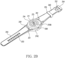
- the electronic device 200 may include at least one of a display 220 (see FIG. 3 ), an audio module 205 and 208, a sensor module 211, a key input device 202, 203 and 204, and a connector hole 209.
- the electronic device 200 may omit at least one of the components (e.g., the key input devices 202, 203 and 204, the connector hole 209, or the sensor module 211) or may further include another component.
- the audio modules 205 and 208 may include a microphone hole 205 and a speaker hole 208.
- a microphone for obtaining external sound may be disposed inside the microphone hole 205, and in some embodiments, a plurality of microphones may be disposed to detect the direction of the sound.
- the speaker hole 208 may be used with an external speaker and a receiver for phone calls.
- the speaker hole 208 and the microphone hole 205 may be implemented as a single hole, or a speaker (e.g., piezo speaker) may be included without the speaker hole 208.
- the key input devices 202, 203, and 204 may include a wheel key 202 disposed on the first surface 210A of the housing 210 and rotatable in at least one direction, and/or side key buttons 203 and 204 disposed on the side surface 210C of the housing 210.
- the wheel key may have a shape corresponding to the shape of the front plate 201.
- the electronic device 200 may not include some or all of the above-described key input devices 202, 203, and 204, and the not included key input devices 202, 203, and 204 may be implemented in other forms such as soft keys on the display 220.
- the connector hole 209 may accommodate a connector (e.g., USB connector) for transmitting and receiving power and/or data to and from external electronic devices and may include another connector hole (not illustrated) capable of accommodating a connector for transmitting and receiving audio signals to and from an external electronic device.
- the electronic device 200 may further include, for example, a connector cover (not illustrated) that covers at least a part of the connector hole 209 and blocks the inflow of external foreign material into the connector hole.
- the binding members 250 and 260 may be detachably attached to at least a part of the housing 210 using locking members 251, 261.
- the binding members 250 and 260 may include one or more of a fixing member 252, a fixing member fastening hole 253, a band guide member 254, and a band fixing ring 255.
- the fixing member 252 may be configured to fix the housing 210 and the binding members 250 and 260 to a part of the user's body (e.g., wrist, ankle, etc.).
- the fixing member fastening hole 253 may correspond to the fixing member 252 to fix the housing 210 and the binding members 250 and 260 to the part of the user's body.
- the band guide member 254 may be configured to limit movement range of the fixing member 252 when the fixing member 252 is fastened to the fixing member fastening hole 253, so that the binding members 250 and 260 are attached to be in close contact with the part of the user's body.
- the band fixing ring 255 may limit the range of movement of the fixing members 250 and 260 when the fixing member 252 and the fixing member fastening hole 253 are fastened.
- FIG. 3 is an exploded perspective view of an electronic device according to an embodiment.
- an electronic device 300 may include a side bezel structure 310, a wheel key 320, a front plate 201, a display 220, a first antenna 350, a second antenna 355, a support member 360 (e.g., bracket), a battery 370, a printed circuit board 380, a sealing member 390, and binding members 395 and 397.
- At least one of the components of the electronic device 300 may be the same as or similar to at least one of the components of the electronic device 200 of FIGS. 1 , 2A , and/or 2B, and repeated description thereof will be omitted.
- the support member 360 may be disposed inside the electronic device 300 to be connected to the side bezel structure 310 or may be integrated with the side bezel structure 310.
- the support member 360 may be made of, for example, metal material and/or non-metal (e.g., polymer) material.
- the display 220 may be coupled to one surface of the support member 360, and the printed circuit board 380 may be coupled to the other surface of the support member 360.
- a processor, a memory, and/or an interface may be mounted on the printed circuit board 380.
- the processor may include, for example, one or more of a central processing unit, an application processor, a graphic processing unit (GPU), an application processor, a sensor processor, or a communication processor.
- the memory may include, for example, a volatile memory or a nonvolatile memory.
- the interface may include, for example, a high definition multimedia interface (HDMI), a universal serial bus (USB) interface, an SD card interface, and/or an audio interface.
- HDMI high definition multimedia interface
- USB universal serial bus
- the interface may electrically or physically connect the electronic device 300 to an external electronic device, for example, and may include a USB connector, an SD card/MMC connector, or an audio connector.
- the battery 370 is a device for supplying power to at least one component of the electronic device 300, and may include, for example, a non-rechargeable primary battery, a rechargeable secondary battery, or a fuel battery. At least a part of the battery 370 may be disposed on substantially the same plane as, for example, the printed circuit board 380.
- the battery 370 may be integrally disposed inside the electronic device 200 or may be detachably coupled to the electronic device 200.
- the first antenna 350 may be disposed between the display 220 and the support member 360.
- the first antenna 350 may include, for example, a near field communication (NFC) antenna, a wireless charging antenna, and/or a magnetic secure transmission (MST) antenna.
- the first antenna 350 may, for example, perform short-range communication with an external device, wirelessly transmit and receive power required for charging, and transmit short-range communication signal or an electromagnetic signal including payment data.
- an antenna structure may be formed by at least a portion of the side bezel structure 310 and/or a part of the support member 360 or a combination thereof.
- the second antenna 355 may be disposed between the printed circuit board 380 and the rear plate 393.
- the second antenna 355 may include, for example, a near field communication (NFC) antenna, a wireless charging antenna, and/or a magnetic secure transmission (MST) antenna.
- NFC near field communication
- MST magnetic secure transmission
- the second antenna 355 may perform short-range communication with an external device, wirelessly transmit and receive power required for charging, and may transmit a short-range communication signal or a electromagnetic signal including payment data.
- an antenna structure may be formed by at least a portion of the side bezel structure 310 and/or a part of the rear plate 393 or a combination thereof.
- the printed circuit board 420 may be electrically connected to various components of the electronic device 400 that perform various operations of the electronic device 400. According to an embodiment, the printed circuit board 420 may be disposed in the inner space 411 formed by the housing 410. According to an embodiment, the printed circuit board 420 may be electrically connected to various electronic components disposed on the printed circuit board 420 or various components of the electronic device 400 disposed outside the printed circuit board 420. According to an embodiment, the printed circuit board 420 may be electrically connected to various components of the electronic device 400 through a connection member (not illustrated).
- the connection member may include a coaxial cable connector, a board to board connector, an interposer, or a flexible printed circuit board (FPCB).
- the plurality of openings 431 may form paths through which light travels into the housing 410, because light blocking material is disposed in region(s) of the layer not corresponding to the plurality of openings 431 and the light blocking material is not disposed in regions of the layer corresponding to the plurality of openings 431.
- the volume of the microvasculature may be changed by changing the amount of blood flow in the microvasculature due to the periodic contraction or relaxation of the heart.
- the degree to which light transmitted to the user's body is absorbed into the body may vary according to the change in the amount of blood flow of the microvasculature.
- the PPG sensor 440 may obtain first biometric data based on the intensity of light reflected from the user's body.
- the PPG sensor 440 may be disposed on the printed circuit board 420 in the housing 410.
- the PPG sensor 440 may include at least one first light emitting portion 441 and at least one first receiving portion 442.
- the first light emitting portion 441 and the first receiving portion 442 may correspond to each other.
- the number of the first light emitting portion 441 and the number of the first receiving portion 442 may be the same, and the first light emitting portion 441 and the first receiving portion 442 having the same number may constitute a PPG sensor 440.
- the number of the first light emitting portion 441 and the number of the first receiving portion 442 may be different from each other, and the first light emitting portion 441 and the first receiving portion 442 having different numbers may constitute a PPG sensor 440.
- the second light emitting portion 451 when the second light emitting portion 451 includes a plurality of laser light sources, the second light emitting portion 451 may simultaneously emit laser beams of different characteristics by changing the wavelengths of the lasers emitted from the plurality of laser light sources by using the modulator.
- the second receiving portion 452 may be configured to receive light emitted from the second light emitting portion 451 and reflected from the part of the user's body. The second receiving portion 452 may generate an electrical signal corresponding to the light reflected from the part of the body. The electrical signal generated by the second receiving portion 452 may be transmitted to the processor (e.g., the processor 120 of FIG. 1 ) through the printed circuit board 420.
- the distance between the second light emitting portion 451 and the second receiving portion 452 may be smaller than the distance between the first light emitting portion 441 and the first receiving portion 442.
- the wavelength range of light emitted from the LED may be wider than the wavelength range of light emitted from the laser light source.
- the wavelength range of light emitted from LEDs configured to emit light of wavelength of 500 nm may be approximately 450 nm to 550 nm, but the wavelength range of light emitted from a laser light source configured to emit light having wavelength of 1300 nm may be approximately 1299 nm to 1301 nm.
- the laser sensor 450 may be disposed on the printed circuit board 420 to be surrounded (or encircled) by the PPG sensor 440.
- at least one first light emitting portion 441 and at least one first receiving portion 442 forming the PPG sensor 440 may surround the periphery of the laser sensor 450.
- at least one first light emitting portion 441 may include a plurality of first light emitting portions 441a, 441b, and 441c that emit light with different wavelengths for the electronic device 400 to obtain various first biometric information.
- a space for disposing the plurality of first light emitting portions 441a, 441b, and 441c in the electronic device 400 that is miniaturized to be worn on a part of the user's body may be insufficient.
- the electronic device 400 may arrange the required number of the plurality of first light emitting portions 441a, 441b, and 441c within the limited internal space of the electronic device 400.
- the laser sensor 450 may be disposed to be surrounded by the PPG sensor 440.
- the electronic device 400 may provide various biometric information to the user by disposing the PPG sensor 440 and the laser sensor 450 having different optical characteristics within a limited internal space of the electronic device.
- the laser sensor 450 may be disposed to overlap the first region 432 of the window 430 when the window 430 is viewed from the outside of the electronic device 400.
- the laser sensor 450 is not disposed in the region of the printed circuit board 420 corresponding to the first region 432 of the window 430, light emitted from the second light emitting portion 451 may not be transmitted to the user's body or the second receiving portion 452 may not receive light.
- the index layer 460 may reduce a difference in refractive index between the inner space 411 and the window 430.
- the index layer 460 may form a path through which light is transmitted from the second light emitting portion 451 to the window 430 or a path through which light is transmitted from the window 430 to the second receiving portion 452.
- the index layer 460 may protect the laser sensor 450 from forces applied from the outside of the electronic device 400.
- the index layer 460 may fill between the second light emitting portion 451 and the window 430 to reduce the difference in refractive index between the window 430 and the second light emitting portion 451 and protect the second light emitting portion 451 from external impacts.
- the index layer 460 may be made of a transparent material and may have elasticity.
- the index layer 460 may be disposed on the laser sensor 450 to overlap the laser sensor 450 when the window 430 is viewed from the outside of the electronic device 400.
- the index layer 460 when the index layer 460 is not used, light emitted from the second light emitting portion 451 may be dispersed, or the light received by the second receiving portion 452 may not receive light, due to the difference in refractive index between the inner space 411 and the window 430.
- performance of the laser sensor 450 may be degraded.
- the PPG sensor 440 of the electronic device 400 may include a plurality of first light emitting portions 441a, 441b, 441c, and 441d and a plurality of first receiving portions 442a, 442b, 442c, and 442d.
- FIG. 5C is a top view illustrating yet another example of an arrangement relationship between a PPG sensor and a laser sensor of an electronic device according to an embodiment.
- the laser sensor 450 may include a plurality of long sides 450a and 450b parallel to each other and a plurality of short sides 450c and 450d that are parallel to each other and have length shorter than that of the plurality of long sides.
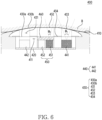
- FIG. 6 is a cross-sectional view illustrating an example in which an electronic device is cut along A-A' of FIG. 4 according to an embodiment.
- the wearing position may be not be secured and may move relative to the user's body.
- the light received by the second receiving portion 452 from the second light emitting portion 451 may include excessive noise, and thus performance of the laser sensor 450 may be degraded.
- the electronic device 400 may be fixed to a particular position on the user's body to ensure performance of the laser sensor 450 by having curvature to maximize the area of contact to the part B of the user's body.
- the first light emitting portion 441 may emit light to the first beam angle ⁇ 1 toward the part B of the user's body.
- the light emitted from the first light emitting portion 441 may sequentially pass through the inner space 411 and the window 430 and pass to the part B of the user's body.
- a part of the light transmitted to the part B of the user's body may be absorbed in the inside (e.g., blood vessels, bones, and cell tissues) of the part B of the user's body.
- Another part of light transmitted to the part B of the user's body may not be absorbed in the part B of the user's body, but may be reflected from the part B of the user's body.
- the second light emitting portion 451 may emit light to a second beam angle ⁇ 2 smaller than the first beam angle ⁇ 1 toward the part B of the user's body.
- the light emitted from the second light emitting portion 451 may sequentially pass through the index layer 460 and the window 430 and may be transmitted to the part B of the user's body.
- a part of the light transmitted to the part B of the user's body may reach a designated material (e.g., glucose molecule or alcohol molecule) in the part B of the user's body.
- the wavelength of light reaching the designated material may be changed by the natural vibration (e.g., Raman scattering) of the designated material, or the intensity of light reaching the designated material may be changed by being absorbed by the designated material.
- the electronic device 400 may arrange the PPG sensor 440 and the laser sensor 450 having different optical characteristics within limited space.
- the electronic device 400 may provide various biometric information to a user by obtaining different first biometric data and second biometric data from the PPG sensor 440 and the laser sensor 450, respectively.
- the electronic device 400 may further include a barrier 470.
- the barrier 470 may prevent crosstalk between light emitted from the second light emitting portion 451 and light received by the second receiving portion 452.
- the barrier 470 may prevent noise from occurring in the laser sensor 450 by preventing crosstalk of light between the second light emitting portion 451 and the second receiving portion 452.
- the barrier 470 may protect the laser sensor 450 from forces applied from the outside of the electronic device 400.
- the barrier 470 may be made of a substantially opaque material so as not to transmit light, but is not limited thereto.
- the barrier 470 may be interposed between the window 430 and the laser sensor 450.
- the barrier 470 may be inserted into the index layer 460 so that it extends between one surface 430a of the window 430 and one surface of the laser sensor 450 facing each other.
- the electronic device 400 may improve the performance of the laser sensor 450 by including the barrier 470 for preventing light crosstalk between the second light emitting portion 451 and the second receiving portion 452.
- the barrier 470 surrounds the outer surface of the index layer 460, light is blocked from transmitting to the outer surface of the index layer 460, so that the performance of the laser sensor 450 may be improved.
- FIG. 9 is a cross-sectional view illustrating a cross-section of an electronic device according to an embodiment.
- the window 930 may include an accommodating groove 935.
- the accommodating groove 935 may receive the index layer 960 and the barrier 970 so as to fix their positions within the electronic device 900.
- the accommodating groove 935 may be formed by recessing one region of the window 930 facing the laser sensor 950 toward the outside of the electronic device 900.
- the accommodating groove 935 may overlap the laser sensor 950.
- the index layer 960 may be inserted into the accommodating groove 935.
- the index layer 960 may extend from one surface of the laser sensor 950 facing the accommodating groove 935 into the accommodating groove 935. As the index layer 960 is seated in the accommodating groove 935, the accommodating groove 935 may prevent the index layer 960 from being separated from the designed position.
- the barrier 970 may be inserted into the accommodating groove 935 and the index layer 960.
- the barrier 970 may extend into the accommodating groove 935 from one surface of the laser sensor 950 facing the accommodating groove 935. As he barrier 970 is seated in the accommodating groove 935, the accommodating groove 935 may prevent the barrier 970 from being separated from the designed position.
- the electronic device 900 may prevent the index layer 960 and the barrier 970 from being separated from their designed positions.
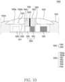
- the window 1030 may include a through hole 1036.
- the through hole 1036 may connect the inner space 1011 of the housing 1010 and the outside of the electronic device 1000.
- the through hole 1036 may extend from one surface 1030a of the window 1030 facing the laser sensor 1050 to the outside of the electronic device 1000.
- FIG. 11 is a cross-sectional view illustrating a cross-section of an electronic device according to an embodiment.
- the barrier 1170 surrounds the outer surfaces of the second light emitting portion 1151 and the second receiving portion 1152, light emitted from the second light emitting portion 1151 or light proceeding to the second receiving portion 1152 may be prevented from being transferred to the inner space 1111. As the transmission of light to the inner space 1111 is prevented, the performance of the laser sensor 1150 may be improved.
- the index layer 1160 may include a Fresnel pattern 1161.
- the Fresnel pattern 1161 may concentrate light.
- the Fresnel pattern 1161 may have a collective shape of a plurality of concentric circles sharing a center.
- the Fresnel pattern 1161 may be formed on one surface of the index layer 1160 facing the laser sensor 1150.
- the Fresnel pattern 1161 may be formed on one surface 1160a of the index layer 1160 facing the second light emitting portion 1151 and the other surface 1160b of the index layer 1160 facing the second receiving portion 1152.
- the surfaces 1160a and 1160b of the index layer 1160 on which the Fresnel pattern 1161 is formed may be referred to as Fresnel lenses.
- Light emitted from the second light emitting unit 1151 may be concentrated by the Fresnel pattern 1161 of one surface 1160a of the index layer 1160 and transmitted to the window 1130.
- Light arriving at the index layer 1160 from the window 1130 may be concentrated by the Fresnel pattern 1161 of the other surface 1160b of the index layer 1160 and received by the second receiving portion 1152.
- the electronic device 1100 may ensure performance of the laser sensor 1150 by concentrating, by the Fresnel pattern 1161, the light emitted from the second light emitting portion 1151 or the light transmitted from the outside of the electronic device 1100 to the second receiving portion 1152.
- an electronic device may comprise a housing (e.g., housing 410 in FIG. 4 ), a printed circuit board (e.g., printed circuit board 420 of FIG. 4 ) disposed within the housing, a window (e.g., window 430 in FIG. 4 ) including a first region (e.g., the first region 432 of FIG. 4 ) parallel to the printed circuit board and a second region (e.g., the second region 433 of FIG.
- a housing e.g., housing 410 in FIG. 4
- a printed circuit board e.g., printed circuit board 420 of FIG. 4
- a window e.g., window 430 in FIG. 4
- a first region e.g., the first region 432 of FIG. 4
- a second region e.g., the second region 433 of FIG.
- a PPG photoplethysmogram
- a PPG sensor e.g., the PPG sensor 440 of FIG. 4
- a laser sensor e.g., the laser sensor 450 of FIG.
- the laser sensor including at least one second emitting portion (e.g., the second light emitting portion 451 of FIG. 4 ) configured to emit light at a second beam angle smaller than the first beam angle toward the window, and at least one second receiving portion (e.g., the second receiving portion 452 of FIG. 4 ) configured to receive light emitted from the at least one second emitting portion and reflected from the part of the user's body and an index layer (e.g., index layer 460 of FIG. 4 ) disposed on the laser sensor; wherein the laser sensor may be disposed on the printed circuit board to be surrounded by the PPG sensor and may overlap the first region, when the window is viewed from an outside of the electronic device.
- the laser sensor may be disposed on the printed circuit board to be surrounded by the PPG sensor and may overlap the first region, when the window is viewed from an outside of the electronic device.
- the PPG sensor may be spaced apart from the laser sensor in a radial direction of the laser sensor.
- the PPG sensor when the window is viewed from the outside of the electronic device, the PPG sensor may overlap the second region.
- the index layer may be interposed between the window and the laser sensor.
- the window further may include a through-hole (e.g., through hole 1036 in FIG. 10 ) extending from one surface (e.g., one surface 1030a of FIG. 10 ) of the window facing the laser sensor to the other surface of the window exposed to the outside of the electronic device, and wherein the index layer is inserted into the through-hole, and one surface of the index layer is exposed to the outside of the electronic device.
- a through-hole e.g., through hole 1036 in FIG. 10
- the window further may include a through-hole (e.g., through hole 1036 in FIG. 10 ) extending from one surface (e.g., one surface 1030a of FIG. 10 ) of the window facing the laser sensor to the other surface of the window exposed to the outside of the electronic device, and wherein the index layer is inserted into the through-hole, and one surface of the index layer is exposed to the outside of the electronic device.
- the window further may include an accommodating groove (e.g., accommodating groove 935 in FIG. 9 ) defined by recessing one region of the window facing the laser sensor toward the outside of the electronic device, and wherein a part of the index layer may be inserted to the accommodating groove.
- an accommodating groove e.g., accommodating groove 935 in FIG. 9
- the at least one first emitting portion may include a plurality of first emitting portions spaced apart from each other along a periphery of the laser sensor, and wherein the at least one first receiving portion may be disposed between the plurality of the first emitting portions along the periphery of the laser sensor.
- the at least one first emitting portion may surround the laser sensor from an outside of the laser sensor, and wherein the at least one first receiving portion may surround the at least one first emitting portion from an outside of the at least one first emitting portion.
- the at least one first emitting portion may include a plurality of first emitting portions each emitting light having different wavelengths
- the at least one second emitting portion may include a plurality of second emitting portions each emitting light having different wavelengths, and wherein a wavelength range of light emitted by the plurality of second emitting portions may be narrower than a wavelength range of light emitted by the plurality of first emitting portions.
- the electronic device may further include a barrier (e.g., the barrier 470 of FIGS. 7A and 7B ) disposed on the laser sensor to be positioned between one region of the window overlapping the at least one second emitting portion and another region of the window overlapping the at least one second receiving portion, when the window is viewed from the outside of the electronic device.
- a barrier e.g., the barrier 470 of FIGS. 7A and 7B
- the barrier may be disposed to surround an outer surface of the index layer.
- the barrier may be between the at least one second receiving portion and the at least one second emitting portion, and extending from the printed circuit board to the window.
- the index layer may be disposed between the barrier and the window, and spaced apart from the laser sensor, and wherein a Fresnel pattern (e.g., the Fresnel pattern 1161 of FIG. 11 ) may be formed on one surface of the index layer facing the laser sensor.
- a Fresnel pattern e.g., the Fresnel pattern 1161 of FIG. 11
- the electronic device further includes a buffering member (e.g., the buffering member 1180 of FIG. 11 ) interposed between the window and the barrier.
- a buffering member e.g., the buffering member 1180 of FIG. 11
- an electronic device may comprise a housing (e.g., the housing 410 in FIG. 4 ) including a first surface (e.g., the first surface 210A of FIG. 2A ), a second surface (e.g., second surface 410b of FIG. 4 ) opposite the first surface and an inner space (e.g., inner space 411 in FIG. 4 ) formed between the first surface and the second surface, a printed circuit board (e.g., the printed circuit board 420 of FIG. 4 ) disposed in the inner space, a window (e.g., the window 430 in FIG.
- a housing e.g., the housing 410 in FIG. 4
- a housing including a first surface (e.g., the first surface 210A of FIG. 2A ), a second surface (e.g., second surface 410b of FIG. 4 ) opposite the first surface and an inner space (e.g., inner space 411 in FIG. 4 ) formed between the first surface and the second surface, a
- a first region e.g., the first region 432 of FIG. 4
- a second region e.g., the second region 433 of FIG. 4
- a PPG photoplethysmogram
- the PPG sensor 440 of FIG. 4 sensor disposed on the printed circuit board and including at least one first emitting portion (e.g., the first light emitting portion 441 of FIG.
- a laser sensor e.g., the laser sensor 450 of FIG. 4
- an index layer e.g., index layer 460 of FIG.
- the laser sensor may be disposed on the printed circuit board to be surrounded by the PPG sensor and may overlap the first region when the window is viewed from the outside of the electronic device.
- the PPG sensor may be spaced apart from the laser sensor in a radial direction of the laser sensor.
- the PPG sensor when the window is viewed from the outside of the electronic device, the PPG sensor may overlap the second region.
- the at least one first emitting portion may include a plurality of first emitting portions spaced apart from each other along a periphery of the laser sensor, and wherein the at least one first receiving portion may be disposed between the plurality of the first emitting portions along the periphery of the laser sensor.
- an element e.g., a first element
- the element may be coupled with the other element directly (e.g., wiredly), wirelessly, or via a third element.
- the machine-readable storage medium may be provided in the form of a non-transitory storage medium.
- non-transitory simply means that the storage medium is a tangible device, and does not include a signal (e.g., an electromagnetic wave), but this term does not differentiate between where data is semi-permanently stored in the storage medium and where the data is temporarily stored in the storage medium.
- a method may be included and provided in a computer program product.
- the computer program product may be traded as a product between a seller and a buyer.
- the computer program product may be distributed in the form of a machine-readable storage medium (e.g., compact disc read only memory (CD-ROM)), or be distributed (e.g., downloaded or uploaded) online via an application store (e.g., PlayStore TM ), or between two user devices (e.g., smart phones) directly. If distributed online, at least part of the computer program product may be temporarily generated or at least temporarily stored in the machine-readable storage medium, such as memory of the manufacturer's server, a server of the application store, or a relay server.
- CD-ROM compact disc read only memory
- an application store e.g., PlayStore TM
- two user devices e.g., smart phones
Landscapes
- Health & Medical Sciences (AREA)
- Life Sciences & Earth Sciences (AREA)
- Physics & Mathematics (AREA)
- Pathology (AREA)
- Cardiology (AREA)
- General Health & Medical Sciences (AREA)
- Surgery (AREA)
- Engineering & Computer Science (AREA)
- Biomedical Technology (AREA)
- Heart & Thoracic Surgery (AREA)
- Medical Informatics (AREA)
- Molecular Biology (AREA)
- Biophysics (AREA)
- Animal Behavior & Ethology (AREA)
- Public Health (AREA)
- Veterinary Medicine (AREA)
- Physiology (AREA)
- Spectroscopy & Molecular Physics (AREA)
- General Physics & Mathematics (AREA)
- Optics & Photonics (AREA)
- Chemical & Material Sciences (AREA)
- Analytical Chemistry (AREA)
- Biochemistry (AREA)
- Immunology (AREA)
- Vascular Medicine (AREA)
- Measuring Pulse, Heart Rate, Blood Pressure Or Blood Flow (AREA)
- Telephone Function (AREA)
Applications Claiming Priority (3)
| Application Number | Priority Date | Filing Date | Title |
|---|---|---|---|
| KR20210142477 | 2021-10-25 | ||
| KR1020210161267A KR20230059095A (ko) | 2021-10-25 | 2021-11-22 | 상이한 광학적 특성을 가지는 복수의 센서들의 성능을 확보하기 위한 구조를 포함하는 전자 장치 |
| PCT/KR2022/009854 WO2023075078A1 (fr) | 2021-10-25 | 2022-07-07 | Dispositif électronique comprenant une structure destinée à faciliter le fonctionnement d'une pluralité de capteurs présentant des caractéristiques optiques différentes |
Publications (4)
| Publication Number | Publication Date |
|---|---|
| EP4394525A1 true EP4394525A1 (fr) | 2024-07-03 |
| EP4394525A4 EP4394525A4 (fr) | 2024-12-11 |
| EP4394525C0 EP4394525C0 (fr) | 2025-08-27 |
| EP4394525B1 EP4394525B1 (fr) | 2025-08-27 |
Family
ID=86055841
Family Applications (1)
| Application Number | Title | Priority Date | Filing Date |
|---|---|---|---|
| EP22887284.2A Active EP4394525B1 (fr) | 2021-10-25 | 2022-07-07 | Dispositif électronique comprenant une structure destinée à faciliter le fonctionnement d'une pluralité de capteurs présentant des caractéristiques optiques différentes |
Country Status (2)
| Country | Link |
|---|---|
| US (1) | US20230131237A1 (fr) |
| EP (1) | EP4394525B1 (fr) |
Family Cites Families (9)
| Publication number | Priority date | Publication date | Assignee | Title |
|---|---|---|---|---|
| TW201309263A (zh) * | 2011-08-19 | 2013-03-01 | 中原大學 | 影像式脈波傳導速度之量測裝置及其量測方法 |
| WO2014178793A1 (fr) * | 2013-04-29 | 2014-11-06 | Heptagon Micro Optics Pte. Ltd. | Bracelet-montre comprenant un oxymètre de pouls intégré ou d'autres modules qui détectent des données physiologiques |
| KR102434698B1 (ko) * | 2015-07-03 | 2022-08-22 | 삼성전자주식회사 | 생체 정보 검출 장치 및 방법 |
| US10702211B2 (en) * | 2016-07-15 | 2020-07-07 | Apple Inc. | Sensor window with integrated isolation feature |
| EP4470456A3 (fr) * | 2017-09-26 | 2025-02-26 | Apple Inc. | Sous-système de capteur optique adjacent à un couvercle d'un boîtier de dispositif électronique |
| JP2022546991A (ja) * | 2019-08-28 | 2022-11-10 | アールディーエス | バイタルサイン又は健康モニタリングシステム及び方法 |
| KR20220129033A (ko) * | 2020-01-13 | 2022-09-22 | 마시모 코오퍼레이션 | 생리학적 파라미터 모니터링 기능이 있는 웨어러블 디바이스 |
| US12089931B1 (en) * | 2020-09-11 | 2024-09-17 | Apple Inc. | Optical sensor for skin-contact detection and physiological parameter measurement at wearable electronic device |
| US11723563B1 (en) * | 2020-09-11 | 2023-08-15 | Apple Inc. | Correcting for emitted light wavelength variation in blood-oxygen saturation measurements at wearable electronic device |
-
2022
- 2022-07-07 EP EP22887284.2A patent/EP4394525B1/fr active Active
- 2022-07-19 US US17/867,800 patent/US20230131237A1/en active Pending
Also Published As
| Publication number | Publication date |
|---|---|
| EP4394525C0 (fr) | 2025-08-27 |
| US20230131237A1 (en) | 2023-04-27 |
| EP4394525B1 (fr) | 2025-08-27 |
| EP4394525A4 (fr) | 2024-12-11 |
Similar Documents
| Publication | Publication Date | Title |
|---|---|---|
| EP4289346B1 (fr) | Dispositif électronique comprenant un ensemble module | |
| US11903733B2 (en) | Electronic device for measuring bio-signals | |
| US20230118495A1 (en) | Wearable electronic device including biometric sensor for measuring body temperature | |
| EP4302683A1 (fr) | Dispositif électronique portable | |
| US20240348093A1 (en) | Electronic device comprising coil assembly | |
| KR20230059095A (ko) | 상이한 광학적 특성을 가지는 복수의 센서들의 성능을 확보하기 위한 구조를 포함하는 전자 장치 | |
| US20240415457A1 (en) | Wearable electronic device including plurality of biometric sensors | |
| US20260114745A1 (en) | Electronic device comprising optical sensor and bio-impedance detection sensor | |
| KR20230059114A (ko) | 센서 모듈을 포함하는 전자 장치 | |
| EP4394525B1 (fr) | Dispositif électronique comprenant une structure destinée à faciliter le fonctionnement d'une pluralité de capteurs présentant des caractéristiques optiques différentes | |
| CN118043745A (zh) | 包括用于促进具有不同光学特性的多个传感器的操作的结构的电子装置 | |
| EP4461210A1 (fr) | Appareil électronique comprenant une pluralité de structures de connexion d'électrodes | |
| CN118973479A (zh) | 包括多个生物特征传感器的可穿戴电子装置 | |
| KR20230140299A (ko) | 복수의 전극 연결 구조를 포함하는 전자 장치 | |
| KR20240148700A (ko) | 센서를 포함하는 웨어러블 장치 | |
| KR20230001147A (ko) | 생체 인식 모듈을 포함하는 전자 장치 | |
| US20250072830A1 (en) | Electronic device including light-emitting structure | |
| KR20220155029A (ko) | 편광을 이용하여 착용을 감지하는 전자 장치 및 방법 | |
| US12386318B2 (en) | Electronic device including biometric recognizing module | |
| EP4666935A1 (fr) | Dispositif portable comprenant un capteur | |
| EP4588434A1 (fr) | Dispositif électronique comprenant une couche de revêtement optique disposée sur un couvercle | |
| KR20230142306A (ko) | 복수의 생체 센서를 포함하는 웨어러블 전자 장치 | |
| KR20250032750A (ko) | 발광 구조물을 포함하는 전자 장치 | |
| KR102899018B1 (ko) | 밴딩 가능한 기판 부재 및 이를 포함하는 전자 장치 | |
| KR20260044724A (ko) | 웨어러블 전자 장치 및 이를 이용한 스펙트럼 조정 방법 |
Legal Events
| Date | Code | Title | Description |
|---|---|---|---|
| STAA | Information on the status of an ep patent application or granted ep patent |
Free format text: STATUS: THE INTERNATIONAL PUBLICATION HAS BEEN MADE |
|
| PUAI | Public reference made under article 153(3) epc to a published international application that has entered the european phase |
Free format text: ORIGINAL CODE: 0009012 |
|
| STAA | Information on the status of an ep patent application or granted ep patent |
Free format text: STATUS: REQUEST FOR EXAMINATION WAS MADE |
|
| 17P | Request for examination filed |
Effective date: 20240326 |
|
| AK | Designated contracting states |
Kind code of ref document: A1 Designated state(s): AL AT BE BG CH CY CZ DE DK EE ES FI FR GB GR HR HU IE IS IT LI LT LU LV MC MK MT NL NO PL PT RO RS SE SI SK SM TR |
|
| A4 | Supplementary search report drawn up and despatched |
Effective date: 20241112 |
|
| RIC1 | Information provided on ipc code assigned before grant |
Ipc: A61B 5/00 20060101ALI20241107BHEP Ipc: A61B 5/021 20060101ALI20241107BHEP Ipc: A61B 5/1455 20060101ALI20241107BHEP Ipc: A61B 5/024 20060101ALI20241107BHEP Ipc: G01N 21/25 20060101ALI20241107BHEP Ipc: G04G 21/02 20100101AFI20241107BHEP |
|
| DAV | Request for validation of the european patent (deleted) | ||
| DAX | Request for extension of the european patent (deleted) | ||
| GRAP | Despatch of communication of intention to grant a patent |
Free format text: ORIGINAL CODE: EPIDOSNIGR1 |
|
| STAA | Information on the status of an ep patent application or granted ep patent |
Free format text: STATUS: GRANT OF PATENT IS INTENDED |
|
| INTG | Intention to grant announced |
Effective date: 20250331 |
|
| GRAS | Grant fee paid |
Free format text: ORIGINAL CODE: EPIDOSNIGR3 |
|
| GRAA | (expected) grant |
Free format text: ORIGINAL CODE: 0009210 |
|
| STAA | Information on the status of an ep patent application or granted ep patent |
Free format text: STATUS: THE PATENT HAS BEEN GRANTED |
|
| AK | Designated contracting states |
Kind code of ref document: B1 Designated state(s): AL AT BE BG CH CY CZ DE DK EE ES FI FR GB GR HR HU IE IS IT LI LT LU LV MC MK MT NL NO PL PT RO RS SE SI SK SM TR |
|
| REG | Reference to a national code |
Ref country code: CH Ref legal event code: EP |
|
| REG | Reference to a national code |
Ref country code: IE Ref legal event code: FG4D |
|
| U01 | Request for unitary effect filed |
Effective date: 20250902 |
|
| U07 | Unitary effect registered |
Designated state(s): AT BE BG DE DK EE FI FR IT LT LU LV MT NL PT RO SE SI Effective date: 20250908 |
|
| PG25 | Lapsed in a contracting state [announced via postgrant information from national office to epo] |
Ref country code: IS Free format text: LAPSE BECAUSE OF FAILURE TO SUBMIT A TRANSLATION OF THE DESCRIPTION OR TO PAY THE FEE WITHIN THE PRESCRIBED TIME-LIMIT Effective date: 20251227 |
|
| PG25 | Lapsed in a contracting state [announced via postgrant information from national office to epo] |
Ref country code: NO Free format text: LAPSE BECAUSE OF FAILURE TO SUBMIT A TRANSLATION OF THE DESCRIPTION OR TO PAY THE FEE WITHIN THE PRESCRIBED TIME-LIMIT Effective date: 20251127 |
|
| PG25 | Lapsed in a contracting state [announced via postgrant information from national office to epo] |
Ref country code: HR Free format text: LAPSE BECAUSE OF FAILURE TO SUBMIT A TRANSLATION OF THE DESCRIPTION OR TO PAY THE FEE WITHIN THE PRESCRIBED TIME-LIMIT Effective date: 20250827 |
|
| PG25 | Lapsed in a contracting state [announced via postgrant information from national office to epo] |
Ref country code: GR Free format text: LAPSE BECAUSE OF FAILURE TO SUBMIT A TRANSLATION OF THE DESCRIPTION OR TO PAY THE FEE WITHIN THE PRESCRIBED TIME-LIMIT Effective date: 20251128 |
|
| PG25 | Lapsed in a contracting state [announced via postgrant information from national office to epo] |
Ref country code: PL Free format text: LAPSE BECAUSE OF FAILURE TO SUBMIT A TRANSLATION OF THE DESCRIPTION OR TO PAY THE FEE WITHIN THE PRESCRIBED TIME-LIMIT Effective date: 20250827 |
|
| PG25 | Lapsed in a contracting state [announced via postgrant information from national office to epo] |
Ref country code: RS Free format text: LAPSE BECAUSE OF FAILURE TO SUBMIT A TRANSLATION OF THE DESCRIPTION OR TO PAY THE FEE WITHIN THE PRESCRIBED TIME-LIMIT Effective date: 20251127 |
|
| PG25 | Lapsed in a contracting state [announced via postgrant information from national office to epo] |
Ref country code: ES Free format text: LAPSE BECAUSE OF FAILURE TO SUBMIT A TRANSLATION OF THE DESCRIPTION OR TO PAY THE FEE WITHIN THE PRESCRIBED TIME-LIMIT Effective date: 20250827 |
|
| PG25 | Lapsed in a contracting state [announced via postgrant information from national office to epo] |
Ref country code: SM Free format text: LAPSE BECAUSE OF FAILURE TO SUBMIT A TRANSLATION OF THE DESCRIPTION OR TO PAY THE FEE WITHIN THE PRESCRIBED TIME-LIMIT Effective date: 20250827 |
|
| PG25 | Lapsed in a contracting state [announced via postgrant information from national office to epo] |
Ref country code: CZ Free format text: LAPSE BECAUSE OF FAILURE TO SUBMIT A TRANSLATION OF THE DESCRIPTION OR TO PAY THE FEE WITHIN THE PRESCRIBED TIME-LIMIT Effective date: 20250827 |
|
| PG25 | Lapsed in a contracting state [announced via postgrant information from national office to epo] |
Ref country code: SK Free format text: LAPSE BECAUSE OF FAILURE TO SUBMIT A TRANSLATION OF THE DESCRIPTION OR TO PAY THE FEE WITHIN THE PRESCRIBED TIME-LIMIT Effective date: 20250827 |