EP4394543A1 - Dispositif électronique comprenant une antenne - Google Patents
Dispositif électronique comprenant une antenne Download PDFInfo
- Publication number
- EP4394543A1 EP4394543A1 EP22870103.3A EP22870103A EP4394543A1 EP 4394543 A1 EP4394543 A1 EP 4394543A1 EP 22870103 A EP22870103 A EP 22870103A EP 4394543 A1 EP4394543 A1 EP 4394543A1
- Authority
- EP
- European Patent Office
- Prior art keywords
- electronic device
- housing
- antenna module
- pads
- disposed
- Prior art date
- Legal status (The legal status is an assumption and is not a legal conclusion. Google has not performed a legal analysis and makes no representation as to the accuracy of the status listed.)
- Pending
Links
Images





Classifications
-
- G—PHYSICS
- G06—COMPUTING OR CALCULATING; COUNTING
- G06F—ELECTRIC DIGITAL DATA PROCESSING
- G06F1/00—Details not covered by groups G06F3/00 - G06F13/00 and G06F21/00
- G06F1/16—Constructional details or arrangements
-
- H—ELECTRICITY
- H01—ELECTRIC ELEMENTS
- H01Q—ANTENNAS, i.e. RADIO AERIALS
- H01Q1/00—Details of, or arrangements associated with, antennas
- H01Q1/12—Supports; Mounting means
- H01Q1/22—Supports; Mounting means by structural association with other equipment or articles
-
- G—PHYSICS
- G06—COMPUTING OR CALCULATING; COUNTING
- G06F—ELECTRIC DIGITAL DATA PROCESSING
- G06F1/00—Details not covered by groups G06F3/00 - G06F13/00 and G06F21/00
- G06F1/16—Constructional details or arrangements
- G06F1/1613—Constructional details or arrangements for portable computers
- G06F1/1633—Constructional details or arrangements of portable computers not specific to the type of enclosures covered by groups G06F1/1615 - G06F1/1626
- G06F1/1684—Constructional details or arrangements related to integrated I/O peripherals not covered by groups G06F1/1635 - G06F1/1675
- G06F1/1698—Constructional details or arrangements related to integrated I/O peripherals not covered by groups G06F1/1635 - G06F1/1675 the I/O peripheral being a sending/receiving arrangement to establish a cordless communication link, e.g. radio or infrared link, integrated cellular phone
-
- G—PHYSICS
- G06—COMPUTING OR CALCULATING; COUNTING
- G06F—ELECTRIC DIGITAL DATA PROCESSING
- G06F3/00—Input arrangements for transferring data to be processed into a form capable of being handled by the computer; Output arrangements for transferring data from processing unit to output unit, e.g. interface arrangements
- G06F3/01—Input arrangements or combined input and output arrangements for interaction between user and computer
- G06F3/03—Arrangements for converting the position or the displacement of a member into a coded form
- G06F3/041—Digitisers, e.g. for touch screens or touch pads, characterised by the transducing means
- G06F3/044—Digitisers, e.g. for touch screens or touch pads, characterised by the transducing means by capacitive means
-
- H—ELECTRICITY
- H01—ELECTRIC ELEMENTS
- H01Q—ANTENNAS, i.e. RADIO AERIALS
- H01Q1/00—Details of, or arrangements associated with, antennas
- H01Q1/12—Supports; Mounting means
- H01Q1/22—Supports; Mounting means by structural association with other equipment or articles
- H01Q1/2258—Supports; Mounting means by structural association with other equipment or articles used with computer equipment
- H01Q1/2266—Supports; Mounting means by structural association with other equipment or articles used with computer equipment disposed inside the computer
-
- H—ELECTRICITY
- H01—ELECTRIC ELEMENTS
- H01Q—ANTENNAS, i.e. RADIO AERIALS
- H01Q21/00—Antenna arrays or systems
- H01Q21/06—Arrays of individually energised antenna units similarly polarised and spaced apart
- H01Q21/08—Arrays of individually energised antenna units similarly polarised and spaced apart the units being spaced along or adjacent to a rectilinear path
-
- G—PHYSICS
- G06—COMPUTING OR CALCULATING; COUNTING
- G06F—ELECTRIC DIGITAL DATA PROCESSING
- G06F3/00—Input arrangements for transferring data to be processed into a form capable of being handled by the computer; Output arrangements for transferring data from processing unit to output unit, e.g. interface arrangements
- G06F3/01—Input arrangements or combined input and output arrangements for interaction between user and computer
- G06F3/03—Arrangements for converting the position or the displacement of a member into a coded form
- G06F3/033—Pointing devices displaced or positioned by the user, e.g. mice, trackballs, pens or joysticks; Accessories therefor
- G06F3/0354—Pointing devices displaced or positioned by the user, e.g. mice, trackballs, pens or joysticks; Accessories therefor with detection of two-dimensional [2D] relative movements between the device, or an operating part thereof, and a plane or surface, e.g. 2D mice, trackballs, pens or pucks
- G06F3/03547—Touch pads, in which fingers can move on a surface
-
- H—ELECTRICITY
- H01—ELECTRIC ELEMENTS
- H01Q—ANTENNAS, i.e. RADIO AERIALS
- H01Q1/00—Details of, or arrangements associated with, antennas
- H01Q1/12—Supports; Mounting means
- H01Q1/22—Supports; Mounting means by structural association with other equipment or articles
- H01Q1/2283—Supports; Mounting means by structural association with other equipment or articles mounted in or on the surface of a semiconductor substrate as a chip-type antenna or integrated with other components into an IC package
Definitions
- Various embodiments of the disclosure relate to an electronic device including an antenna.
- an electronic device may include antenna modules capable of fast, high-capacity transmission to produce and transmit various contents, connect various objects to the Internet (for example, Internet of things (IoT)), or connect communication among various sensors for autonomous driving.
- an electronic device may include an antenna module (hereinafter, an mm Wave antenna module) to emit mm Wave signals.
- an mmWave antenna module may be disposed in a touch pad area.
- a structure of a part of an area of a touch pad where an antenna module is disposed may be changed to a structure for guaranteeing an antenna radiation path.
- an electronic device may include: a housing which forms at least a part of an exterior of the electronic device; an antenna module which is disposed in the housing and includes a first surface facing one surface of the housing and a second surface facing in the opposite direction of the first surface, the antenna module including an antenna array disposed on the first surface; a wireless communication circuit electrically connected with the antenna module; an insulation layer which is disposed between the first surface of the antenna module and one surface of the housing; and first pads which are disposed in a first area of the insulation layer that corresponds to the first surface of the antenna module, and each of the first pads may have a first shape in which at least a part of an area overlapping the antenna array is removed, and the wireless communication circuit may feed power to the antenna array, thereby transmitting and/or receiving a signal of a designated frequency band.
- an electronic device may include: a display; a housing including a first housing coupled with the display, and a second housing coupled to be rotatable relative to the first housing through the hinge structure and including a cover layer; an antenna module which is disposed in the second housing and includes a first surface facing the cover layer and a second surface facing in the opposite direction of the first surface, the antenna module including an antenna array disposed on the first surface; a wireless communication circuit electrically connected with the antenna module; an insulation layer which is disposed between the first surface of the antenna module and the cover layer; and first pads which are disposed in a first area of the insulation layer that corresponds to the first surface of the antenna module, and each of the first pads may have a first shape in which at least a part of an area overlapping the antenna array is removed, and the wireless communication circuit may feed power to the antenna array, thereby transmitting and/or receiving a signal of a designated frequency band.
- At least a part of an area that corresponds to an area where an antenna module is disposed among areas of a touch pad has a specific shape, so that degradation of radiation performance of an antenna module may be reduced.
- an antenna module is disposed in an area that is adjacent to a periphery among areas of a touch pad, so that reduction of usability of a touch pad may be minimized.
- Fig. 1 is a block diagram illustrating an electronic device 101 in a network environment 100 according to various embodiments.
- the electronic device 101 in the network environment 100 may communicate with an electronic device 102 via a first network 198 (e.g., a short-range wireless communication network), or at least one of an electronic device 104 or a server 108 via a second network 199 (e.g., a long-range wireless communication network).
- the electronic device 101 may communicate with the electronic device 104 via the server 108.
- the electronic device 101 may include a processor 120, memory 130, an input module 150, a sound output module 155, a display module 160, an audio module 170, a sensor module 176, an interface 177, a connecting terminal 178, a haptic module 179, a camera module 180, a power management module 188, a battery 189, a communication module 190, a subscriber identification module(SIM) 196, or an antenna module 197.
- at least one of the components e.g., the connecting terminal 178) may be omitted from the electronic device 101, or one or more other components may be added in the electronic device 101.
- some of the components e.g., the sensor module 176, the camera module 180, or the antenna module 197) may be implemented as a single component (e.g., the display module 160).
- the processor 120 may execute, for example, software (e.g., a program 140) to control at least one other component (e.g., a hardware or software component) of the electronic device 101 coupled with the processor 120, and may perform various data processing or computation. According to one embodiment, as at least part of the data processing or computation, the processor 120 may store a command or data received from another component (e.g., the sensor module 176 or the communication module 190) in volatile memory 132, process the command or the data stored in the volatile memory 132, and store resulting data in non-volatile memory 134.
- software e.g., a program 140
- the processor 120 may store a command or data received from another component (e.g., the sensor module 176 or the communication module 190) in volatile memory 132, process the command or the data stored in the volatile memory 132, and store resulting data in non-volatile memory 134.
- the processor 120 may include a main processor 121 (e.g., a central processing unit (CPU) or an application processor (AP)), or an auxiliary processor 123 (e.g., a graphics processing unit (GPU), a neural processing unit (NPU), an image signal processor (ISP), a sensor hub processor, or a communication processor (CP)) that is operable independently from, or in conjunction with, the main processor 121.
- a main processor 121 e.g., a central processing unit (CPU) or an application processor (AP)
- auxiliary processor 123 e.g., a graphics processing unit (GPU), a neural processing unit (NPU), an image signal processor (ISP), a sensor hub processor, or a communication processor (CP)
- the main processor 121 may be adapted to consume less power than the main processor 121, or to be specific to a specified function.
- the auxiliary processor 123 may be implemented as separate from, or as part of the main processor 121.
- the auxiliary processor 123 may control at least some of functions or states related to at least one component (e.g., the display module 160, the sensor module 176, or the communication module 190) among the components of the electronic device 101, instead of the main processor 121 while the main processor 121 is in an inactive (e.g., sleep) state, or together with the main processor 121 while the main processor 121 is in an active state (e.g., executing an application).
- the auxiliary processor 123 e.g., an image signal processor or a communication processor
- the memory 130 may store various data used by at least one component (e.g., the processor 120 or the sensor module 176) of the electronic device 101.
- the various data may include, for example, software (e.g., the program 140) and input data or output data for a command related thererto.
- the memory 130 may include the volatile memory 132 or the non-volatile memory 134.
- the program 140 may be stored in the memory 130 as software, and may include, for example, an operating system (OS) 142, middleware 144, or an application 146.
- OS operating system
- middleware middleware
- application application
- the input module 150 may receive a command or data to be used by another component (e.g., the processor 120) of the electronic device 101, from the outside (e.g., a user) of the electronic device 101.
- the input module 150 may include, for example, a microphone, a mouse, a keyboard, a key (e.g., a button), or a digital pen (e.g., a stylus pen).
- the sound output module 155 may output sound signals to the outside of the electronic device 101.
- the sound output module 155 may include, for example, a speaker or a receiver.
- the speaker may be used for general purposes, such as playing multimedia or playing record.
- the receiver may be used for receiving incoming calls. According to an embodiment, the receiver may be implemented as separate from, or as part of the speaker.
- the display module 160 may visually provide information to the outside (e.g., a user) of the electronic device 101.
- the display module 160 may include, for example, a display, a hologram device, or a projector and control circuitry to control a corresponding one of the display, hologram device, and projector.
- the display module 160 may include a touch sensor adapted to detect a touch, or a pressure sensor adapted to measure the intensity of force incurred by the touch.
- the audio module 170 may convert a sound into an electrical signal and vice versa. According to an embodiment, the audio module 170 may obtain the sound via the input module 150, or output the sound via the sound output module 155 or a headphone of an external electronic device (e.g., an electronic device 102) directly (e.g., wiredly) or wirelessly coupled with the electronic device 101.
- an external electronic device e.g., an electronic device 102
- directly e.g., wiredly
- wirelessly e.g., wirelessly
- the sensor module 176 may detect an operational state (e.g., power or temperature) of the electronic device 101 or an environmental state (e.g., a state of a user) external to the electronic device 101, and then generate an electrical signal or data value corresponding to the detected state.
- the sensor module 176 may include, for example, a gesture sensor, a gyro sensor, an atmospheric pressure sensor, a magnetic sensor, an acceleration sensor, a grip sensor, a proximity sensor, a color sensor, an infrared (IR) sensor, a biometric sensor, a temperature sensor, a humidity sensor, or an illuminance sensor.
- the battery 189 may supply power to at least one component of the electronic device 101.
- the battery 189 may include, for example, a primary cell which is not rechargeable, a secondary cell which is rechargeable, or a fuel cell.
- the communication module 190 may include a wireless communication module 192 (e.g., a cellular communication module, a short-range wireless communication module, or a global navigation satellite system (GNSS) communication module) or a wired communication module 194 (e.g., a local area network (LAN) communication module or a power line communication (PLC) module).
- a wireless communication module 192 e.g., a cellular communication module, a short-range wireless communication module, or a global navigation satellite system (GNSS) communication module
- GNSS global navigation satellite system
- wired communication module 194 e.g., a local area network (LAN) communication module or a power line communication (PLC) module.
- LAN local area network
- PLC power line communication
- each of such phrases as “A or B,” “at least one of A and B,” “at least one of A or B,” “A, B, or C,” “at least one of A, B, and C,” and “at least one of A, B, or C,” may include any one of, or all possible combinations of the items enumerated together in a corresponding one of the phrases.
- such terms as “1st” and “2nd,” or “first” and “second” may be used to simply distinguish a corresponding component from another, and does not limit the components in other aspect (e.g., importance or order).
- module may include a unit implemented in hardware, software, or firmware, and may interchangeably be used with other terms, for example, “logic,” “logic block,” “part,” or “circuitry”.
- a module may be a single integral component, or a minimum unit or part thereof, adapted to perform one or more functions.
- the module may be implemented in a form of an application-specific integrated circuit (ASIC).
- ASIC application-specific integrated circuit
- each component e.g., a module or a program of the above-described components may include a single entity or multiple entities, and some of the multiple entities may be separately disposed in different components. According to various embodiments, one or more of the above-described components may be omitted, or one or more other components may be added. Alternatively or additionally, a plurality of components (e.g., modules or programs) may be integrated into a single component. In such a case, according to various embodiments, the integrated component may still perform one or more functions of each of the plurality of components in the same or similar manner as they are performed by a corresponding one of the plurality of components before the integration.
- operations performed by the module, the program, or another component may be carried out sequentially, in parallel, repeatedly, or heuristically, or one or more of the operations may be executed in a different order or omitted, or one or more other operations may be added.
- the electronic device 101 may further include at least one of the components illustrated in FIG. 1
- the network 199 may further include at least one other network.
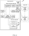
- the first communication processor 212, the second communication processor 214, the first RFIC 222, the second RFIC 224, the fourth RFIC 228, the first RFFE 232, and the second RFFE 234 may form at least part of a wireless communication module 192.
- the fourth RFIC 228 may be omitted or may be included as part of the third RFIC 226.
- the first RFIC 222 may convert a baseband signal, which is generated by the first communication processor 212, into a radio frequency (RF) signal of about 700 MHz to about 3 GHz to be used in the first network 292 (for example, a legacy network).
- RF radio frequency
- an RF signal may be acquired from the first network 292 (for example, a legacy network) via an antenna (for example, the first antenna module 242), and may be pre-processed through an RFFE (for example, the first RFFE 232).
- the first RFIC 222 may convert the pre-processed RF signal into a baseband signal to be processed by the first communication processor 212.
- the third RFIC 226 may convert a baseband signal, which is generated by the second communication processor 214, into an RF signal (hereinafter, a 5G Above6 RF signal) of a 5G Above6 band (for example, about 6 GHz to about 60 GHz) to be used in the second network 294 (for example, a 5G network).
- a 5G Above6 RF signal may be acquired from the second network 294 (for example, a 5G network) via an antenna (for example, the antenna 248), and may be pre-processed through the third RFFE 236.
- the third RFIC 226 may convert the pre-processed 5G Above6 RF signal into a baseband signal to be processed by the second communication processor 214.
- the third RFFE 236 may be formed as part of the third RFIC 226.
- the electronic device 101 may include the fourth RFIC 228 separately from or as part of the third RFIC 226.
- the fourth RFIC 228 may convert a baseband signal, which is generated by the second communication processor 214, into an RF signal of an intermediate frequency band (for example, about 9 GHz to about 11 GHz) (hereinafter, an IF signal), and then may transfer the IF signal to the third RFIC 226.
- the third RFIC 226 may convert the IF signal into a 5G Above6 RF signal.
- a 5G Above6 RF signal may be received from the second network 294 (for example, a 5G network) via an antenna (for example, the antenna 248), and may be converted into an IF signal by the third RFIC 226.
- the fourth RFIC 228 may convert the IF signal into a baseband signal to be processed by the second communication processor 214.
- the third RFIC 226 and the antenna 248 may be disposed on the same substrate to form a third antenna module 246.
- the wireless communication module 192 or the processor 120 may be disposed on a first substrate (for example, a main PCB).
- the third antenna module 246 may be formed by the third RFIC 226 being disposed on an area (for example, a lower surface) of a second substrate (for example, a sub PCB) separate from the first substrate, and the antenna 948 being disposed on another area (for example, an upper surface).
- the third RFIC 226 and the antenna 248 may be disposed on the same substrate, so that a length of a transmission line therebetween may be reduced.
- This may reduce a loss (for example, attenuation) of a signal of a high frequency band (for example, about 6 GHz to about 60 GHz) used for 5G network communication, which is caused by a transmission line. Accordingly, the electronic device 101 may enhance quality or speed of communication with the second network 294 (for example, the 5G network).
- a loss for example, attenuation
- a high frequency band for example, about 6 GHz to about 60 GHz
- the electronic device 101 may enhance quality or speed of communication with the second network 294 (for example, the 5G network).
- the antenna 248 may be formed as an antenna array including a plurality of antenna elements to be used for beamforming.
- the third RFIC 226 may include a plurality of phase shifters 238 corresponding to the plurality of antenna elements, as part of the third RFFE 236.
- the plurality of phase shifters 238 may shift phases of 5G Above6 RF signals to be transmitted to the outside (for example, a base station of a 5G network) of the electronic device 101 via corresponding antenna elements.
- the plurality of phase shifters 238 may shift phases of 5G Above6 RF signals received from the outside through corresponding antenna elements to the same phases or substantially the same phases. This makes it possible to transmit or receive through beamforming between the electronic device 101 and the outside.
- the second network 294 may be operated independently from the first network 292 (for example, a legacy network) (for example, stand-alone (SA)), or may be operated in conjunction therewith (for example, non-stand alone (NSA)).
- the 5G network may include only an access network (for example, a 5G radio access network (RAN) or a next generation RAN (NG RAN)), and may not include a core network (for example, a next generation core (NGC)).
- the electronic device 101 may access an external network (for example, Internet) under control of the core network (for example, an evolved packed core (EPC)) of the legacy network.
- EPC evolved packed core
- Protocol information for example, LTE protocol information
- protocol information for example, new radio (NR) protocol information
- 5G network may be stored in the memory 230, and may be accessed by other components (for example, the processor 120, the first communication processor 212, or the second communication processor 214).
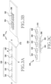
- FIG. 3 illustrates an embodiment of the structure of the third antenna module 246 described with reference to FIG. 2 .
- FIG. 3A is a perspective view of the third antenna module 246 as viewed from one side
- FIG. 3B is a perspective view of the third antenna module 246 as viewed from the other side.
- FIG. 3C is a cross-sectional view taken on line A-A', illustrating the third antenna module 246.
- the third antenna module 246 may include a printed circuit board 310, an antenna array 330, a radio frequency integrate circuit (RFIC) 352, a power manage integrate circuit (PMIC) 354, and a module interface 370.
- the third antenna module 246 may further include a shielding member 390.
- at least one of the aforementioned components may be omitted or at least two of the aforementioned components may be integrated.
- the printed circuit board 310 may include a plurality of conductive layers and a plurality of nonconductive layers which are stacked alternately with the conductive layers.
- the printed circuit board 310 may provide electrical connection between the printed circuit board 310 and/or various electronic components disposed outside by using wires and conductive vias which are formed on the conductive layer.
- the antenna array 330 may include a plurality of antenna elements 332, 333, 334, 336, or 338 disposed to form a directional beam.
- the antenna elements may be formed on a first surface of the printed circuit board 310 as shown in the drawings.
- the antenna array 330 may be disposed inside the printed circuit board 310.
- the antenna array 330 may include a plurality of antenna arrays of the same or different shapes or kinds (for example, a dipole antenna array and/or a patch antenna array).
- the RFIC 352 may be disposed on another area (for example, a second surface opposite to the first surface) of the printed circuit board 310 that is spaced apart from the antenna array.
- the RFIC may be configured to process a signal of a selected frequency band which is transmitted/received through the antenna array 330.
- the RFIC 352 when transmitting signals, may convert a baseband signal acquired from a communication processor (not shown) into an RF signal of a designated band.
- the RFIC 352 may convert an RF signal received through the antenna array 352 into a baseband signal, and may transmit the signal to the communication processor.
- the RFIC 352 when transmitting signals, may up-convert an IF signal (for example, about 9 GHz to about 11 GHz) acquired from an intermediate frequency integrate circuit (IFIC) (for example, 228 of FIG. 2 ) into an RF signal of a selected band.
- IFIC intermediate frequency integrate circuit
- the RFIC 352 may down-convert an RF signal acquired through the antenna array 352 into an IF signal, and may transmit the signal to the IFIC.
- the PMIC 354 may be disposed on a part of another area (for example, the second surface) of the printed circuit board 310, which is spaced apart from the antenna array.
- the PMIC may receive a voltage from a main PCB (not shown) and may provide necessary power to various components (for example, the RFIC 352) on the antenna module.
- the shielding member 390 may be disposed on a part (for example, the second surface) of the printed circuit board 310 to electromagnetically shield at least one of the RFIC 352 or the PMIC 354.
- the shielding member 390 may include a shield can.
- the third antenna module 246 may be electrically connected with another printed circuit board (for example, a major circuit board) through the module interface although the module interface is not illustrated.
- the module interface may include a connection member, for example, a coaxial cable connector, a board-to-board connector, an interposer, or a flexible printed circuit board (FPCB).
- the RFIC 352 and/or the PMIC 354 of the antenna module may be electrically connected with the printed circuit board through the connection member.
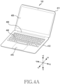
- FIG. 4A illustrates an unfolding state of an electronic device according to an embodiment.
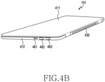
- FIG. 4B illustrates a folding state of the electronic device according to an embodiment.
- the second housing 412 may be connected to be rotatable relative to the first housing 411.
- the first housing 411 and the second housing 412 may be connected through the hinge structure 430.
- the second housing 412 may rotate relative to the first housing 411 with reference to a first axis (for example, a y-axis).
- the first housing 411 and the second housing 412 may be disposed on both sides with reference to the first axis (for example, the y-axis), and may be symmetric with reference to the first axis.
- the shapes of the first housing 411 and the second housing 412 may not be limited to the symmetric shape and at least a part of the first housing 411 and the second housing 412 may be asymmetrical with respect to the first axis.
- the keyboard 440 may be disposed on one surface of the second housing 412.
- the touch pad 470 may be disposed on one surface of the second housing 412.
- the keyboard 440 and the touch pad 470 may be disposed on the same surface of the second housing 412.
- the touch pad 470 may be positioned in a first direction (for example, a -x direction) relative to the keyboard 440.
- the touch pad 470 may identify a touch input of a user by using a touch detection sensor coupled with the touch pad 470.
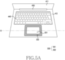
- the electronic device 101 may include a first housing 411, a second housing 412, a hinge structure 430, a keyboard 440 disposed in the second housing 412, and a cover layer 550 which is included in a touch pad (for example, the touch pad 470 of FIG. 4A ) and has at least a part exposed to the outside of the electronic device 101.
- a touch pad for example, the touch pad 470 of FIG. 4A
- the same reference numerals may be used for components that are the same or substantially the same as the above-described components, and a redundant explanation is omitted.
- the touch pad 470 may be disposed on one surface of the second housing 412. According to an embodiment, a part of the second housing 412 may be formed as the touch pad 470. According to an embodiment, the touch pad 470 may be formed with a nonconductive material (for example, plastic), but this should not be considered as limiting.
- the cover layer 550 may include a first touch area 551 and a second touch area 552 which is extended from the first touch area 551.
- the cover layer 550 may include a first touch area 551 which is adjacent to the center of the cover layer 550, and a second touch area 552 which is extended from the first touch area 551 and is adjacent to a periphery of the cover layer 550.
- an insulation layer 510 and an antenna module 530 may be disposed under the cover layer 550.
- the insulation layer 510 may be disposed in an area corresponding to the cover layer 550.
- the antenna module 530 may be disposed under the insulation layer 510.
- the antenna module 530 may be disposed in an area corresponding to the second touch area 552 of the cover layer 550 under the insulation layer 510.
- the insulation layer 510 may be formed with a nonconductive material.
- the insulation layer 510 may be formed with a high molecular material (for example, resin) and/or fiberglass.
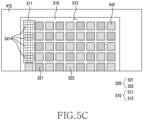
- a plurality of pads 520 may be disposed on one surface of the insulation layer 510 that is adjacent to the cover layer 510 according to an embodiment.
- the plurality of pads 520 may include a reception pad 521 having a negative voltage and a transmission pad 522 having a positive voltage.
- at least one processor may detect a touch input of a user on the touch pad 470 by detecting a change in the capacitance of the reception pad 521 and the transmission pad 522.
- at least a part of the reception pad 521 and the reception pad 522 may be electrically connected with the ground.
- the reception pad 521 and the transmission pad 522 may be disposed alternately on the insulation layer 510.
- arrangements of the reception pad 521 and the transmission pad 522 are not limited to the above-described example.
- the insulation layer 510 may include a first area 511 corresponding to one surface of the antenna module 530, and a second area 512 other than the first area 511.
- the plurality of pads 541 and 542 may include first pads 541 which are disposed on the first area 511 of the insulation layer 510, and second pads 542 which are disposed on the second area 512 of the insulation layer 510.
- the first pads 541 and the second pads 542 may have different shapes and/or areas.
- each of the first pads 541 may have a first shape in which at least a part of an area overlapping an antenna array disposed in the antenna module 530 is removed.
- the first shape of the first pads 541 may have a mesh pattern, but this should not be considered as limiting.
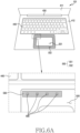
- FIG. 6A illustrates a front surface of an electronic device according to an embodiment, and an enlarged view thereof.
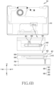
- FIG. 6B illustrates an enlarged view of the electronic device including a fixing structure according to an embodiment, and a cross-sectional view taken along the C axis.
- the electronic device 101 may include a first housing 411, a second housing 412, a display 420, a hinge structure 430, a keyboard 440, a cover layer 550 which is included a touch pad (for example, the touch pad 470 of FIG. 4A ) and has at least a part exposed to the outside of the electronic device 101, and an antenna module 530 disposed under the cover layer 550.
- the electronic device 101 may include a fixing structure 620, 630 to fix the antenna module 530 to the second housing 412.
- the same reference numerals may be used for the same components as the above-described components, and a redundant explanation is omitted.
- the antenna module 530 may be disposed under the cover layer 550. According to an embodiment, the antenna module 530 may be disposed under the cover layer 550 in an area that is adjacent to a periphery of the cover layer 550. According to an embodiment, the antenna module 530 may be disposed under an area of the cover layer 550 that corresponds to a second touch area 552.
- the antenna module 530 may be coupled with at least a part of the second housing 412 through the fixing structure 620, 630. According to an embodiment, the antenna module 530 may be coupled with at least a part of the second housing 412 through the fixing structure 620, 630, and may be disposed under the cover layer 550 of the touch pad (for example, the touch pad 470 of FIG. 4A ).
- the fixing structure 620, 630 may include a first fixing structure 620 and a second fixing structure 630 which is spaced apart from the first fixing structure 620.
- the first fixing structure 620 may include a first protrusion 621 which is extended from one end of the antenna module 530 in a first direction (for example, a +x direction), and a first coupling member 622 which is coupled with the first protrusion 621 to fix the antenna module 530 to the second housing 412.
- the second fixing structure 630 may include a second protrusion 631 which is extended from one end of the antenna module 530 in a second direction (for example, a +y direction) substantially perpendicular to the first direction, and a second coupling member 632 which is coupled with the second protrusion 631 to fix the antenna module 530 to the second housing 412.
- a second direction for example, a +y direction
- the direction and position in which the fixing structure 620 is formed are not limited to the above-described example, and the fixing structure 620 may be formed in various directions and positions.
- a printed circuit board 710 (for example, the printed circuit board 310 of FIG. 3 ) according to an embodiment may include an antenna array 730 disposed on one surface thereof.
- the antenna array 730 according to an embodiment may be referred to as at least a part of the antenna array 330 of FIG. 3 .
- a wireless communication circuit (for example, the wireless communication module 192 of FIG. 1 ) electrically connected with the printed circuit board 710 may feed power to the antenna array 730, thereby transmitting and/or receiving a signal of a designated frequency band (for example, 3.5 GHz).
- the reception pad 741 and/or transmission pad 742 may have a shape in which at least a part of an area overlapping the antenna array 730 is removed.
- the reception pad 741 and/or transmission pad 742 may have a mesh pattern.
- the reception pad 741 and/or transmission pad 742 may have a shape in which some areas of the mesh pattern are filled, but the shape of the reception pad 741 and the transmission pad 742 is not limited to the above-described example and may be referred to as various shapes.
- RF radio frequency
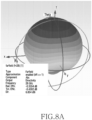
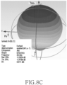
- radiation performance of a RF signal achieved through the antenna array 730 when at least a part of the printed circuit board 710 according to an embodiment overlaps the reception pad 741 or the transmission pad 742 may be identified.
- radiation performance of a signal achieved through the antenna array 730 when at least a part of the printed circuit board 710 overlaps the reception pad 741 or the transmission pad 742 may be similar to or substantially the same as radiation performance of a signal achieved through the antenna array 730 when at least a part of the printed circuit board 710 does not overlap the reception pad 741 or the transmission pad 742.
- radiation performance of a RF signal achieved when at least a part of the printed circuit board 710 and the antenna array 730 overlaps the reception pad 741 or the transmission pad 742 may not be degraded compared to radiation performance of a RF signal achieved when at least a part of the printed circuit board 710 and the antenna array 730 does not overlap the reception pad 741 or the transmission pad 742.
- the transmission pad 522 and the reception pad 521 may be alternately arranged on the insulation layer 510.
- the electronic device 101 may further include a fixing structure coupled with at least a part of the antenna module 530, and the antenna module 530 may be coupled with the housing and/or the insulation layer 510 through the fixing structure.
Landscapes
- Engineering & Computer Science (AREA)
- Theoretical Computer Science (AREA)
- General Engineering & Computer Science (AREA)
- Computer Hardware Design (AREA)
- Human Computer Interaction (AREA)
- Physics & Mathematics (AREA)
- General Physics & Mathematics (AREA)
- Transceivers (AREA)
Applications Claiming Priority (2)
| Application Number | Priority Date | Filing Date | Title |
|---|---|---|---|
| KR1020210123989A KR20230040625A (ko) | 2021-09-16 | 2021-09-16 | 안테나를 포함하는 전자 장치 |
| PCT/KR2022/009374 WO2023043016A1 (fr) | 2021-09-16 | 2022-06-30 | Dispositif électronique comprenant une antenne |
Publications (2)
| Publication Number | Publication Date |
|---|---|
| EP4394543A1 true EP4394543A1 (fr) | 2024-07-03 |
| EP4394543A4 EP4394543A4 (fr) | 2024-12-18 |
Family
ID=85603090
Family Applications (1)
| Application Number | Title | Priority Date | Filing Date |
|---|---|---|---|
| EP22870103.3A Pending EP4394543A4 (fr) | 2021-09-16 | 2022-06-30 | Dispositif électronique comprenant une antenne |
Country Status (4)
| Country | Link |
|---|---|
| US (1) | US12482917B2 (fr) |
| EP (1) | EP4394543A4 (fr) |
| KR (1) | KR20230040625A (fr) |
| WO (1) | WO2023043016A1 (fr) |
Family Cites Families (15)
| Publication number | Priority date | Publication date | Assignee | Title |
|---|---|---|---|---|
| JP5118666B2 (ja) * | 2009-06-17 | 2013-01-16 | アルプス電気株式会社 | アンテナ付タッチパッド入力装置、及び該装置を搭載した電子機器 |
| JP2011138403A (ja) | 2009-12-28 | 2011-07-14 | Sony Corp | 情報処理装置 |
| TWI505553B (zh) | 2012-06-21 | 2015-10-21 | Wistron Neweb Corp | 多功能射頻裝置、電腦系統及多功能射頻裝置操作方法 |
| TWI436252B (zh) | 2012-12-19 | 2014-05-01 | Chih Chung Lin | 觸控板製造方法 |
| CN105552561A (zh) * | 2012-12-21 | 2016-05-04 | 株式会社村田制作所 | 接口单元以及计算机 |
| US10622703B2 (en) | 2014-03-05 | 2020-04-14 | Samsung Electronics Co., Ltd | Antenna device and electronic device having the antenna device |
| KR102248849B1 (ko) | 2014-03-05 | 2021-05-07 | 삼성전자주식회사 | 안테나 장치 및 그를 구비하는 전자 장치 |
| KR20160051136A (ko) * | 2014-10-31 | 2016-05-11 | 삼성전기주식회사 | 터치센서 모듈 |
| US20170139520A1 (en) | 2015-11-17 | 2017-05-18 | Jtouch Corporation | Metal mesh touch module with transparent antenna and touch display apparatus using same |
| JP6778650B2 (ja) * | 2017-05-16 | 2020-11-04 | アルプスアルパイン株式会社 | アンテナ付きタッチパッド |
| KR102580708B1 (ko) | 2018-12-05 | 2023-09-21 | 삼성전자주식회사 | 인쇄 회로 기판의 일면을 통해 외부로 드러나는 신호선을 포함하고, 상기 신호선과 전기적으로 연결된 도전부재를 포함하는 안테나 모듈 및 이를 포함하는 전자 장치 |
| KR102671154B1 (ko) * | 2018-12-31 | 2024-05-30 | 엘지디스플레이 주식회사 | 안테나 일체형 표시장치 |
| US11281340B2 (en) * | 2019-01-18 | 2022-03-22 | Cirque Corporation | Radio frequency transparent capacitive touch systems and methods |
| KR102262747B1 (ko) * | 2019-04-04 | 2021-06-08 | 동우 화인켐 주식회사 | 터치 센서-안테나 모듈 및 이를 포함하는 디스플레이 장치 |
| KR102225524B1 (ko) | 2019-11-08 | 2021-03-08 | 동우 화인켐 주식회사 | 터치 센서를 포함하는 안테나 모듈 및 이를 포함하는 디스플레이 장치 |
-
2021
- 2021-09-16 KR KR1020210123989A patent/KR20230040625A/ko active Pending
-
2022
- 2022-06-30 WO PCT/KR2022/009374 patent/WO2023043016A1/fr not_active Ceased
- 2022-06-30 EP EP22870103.3A patent/EP4394543A4/fr active Pending
-
2024
- 2024-03-15 US US18/606,409 patent/US12482917B2/en active Active
Also Published As
| Publication number | Publication date |
|---|---|
| WO2023043016A1 (fr) | 2023-03-23 |
| KR20230040625A (ko) | 2023-03-23 |
| EP4394543A4 (fr) | 2024-12-18 |
| US12482917B2 (en) | 2025-11-25 |
| US20240250406A1 (en) | 2024-07-25 |
Similar Documents
| Publication | Publication Date | Title |
|---|---|---|
| US20250286943A1 (en) | Structure for applying millimeter wave antenna module to foldable electronic device | |
| EP4167374B1 (fr) | Dispositif et procédé pour améliorer les performances d'une antenne à ondes millimétriques dans un dispositif électronique comprenant un boîtier en céramique | |
| US12548886B2 (en) | Electronic device comprising antenna | |
| EP4340125A1 (fr) | Dispositif électronique comprenant une antenne | |
| US11705619B2 (en) | Antenna and electronic device including the same | |
| US20240322419A1 (en) | Electronic device comprising antenna module | |
| US12341265B2 (en) | Electronic apparatus comprising antenna | |
| US12132250B2 (en) | Antenna module and electronic device including the same | |
| EP4277031B1 (fr) | Dispositif électronique comprenant un module d'antenne | |
| US11687128B2 (en) | Electronic device including flexible display and antenna | |
| US11784395B2 (en) | Grip detection method and electronic device supporting same | |
| US12469958B2 (en) | Electronic device including structure in which key button and antenna module overlap | |
| US12294140B2 (en) | Electronic device comprising antenna | |
| US12212068B2 (en) | Electronic device including antenna module | |
| US20230187849A1 (en) | Antenna and electronic device comprising same | |
| EP4394543A1 (fr) | Dispositif électronique comprenant une antenne | |
| EP4415171A1 (fr) | Dispositif électronique comprenant une antenne | |
| EP4579952A1 (fr) | Dispositif électronique comprenant une antenne | |
| US20240429593A1 (en) | Electronic device comprising antenna and segment structure | |
| EP4425710A1 (fr) | Dispositif électronique comprenant un câble rf | |
| US20250294087A1 (en) | Electronic device comprising structure for reducing damage to electromagnetic induction panel | |
| US20240186681A1 (en) | Mobile communication device comprising antenna | |
| US20250130533A1 (en) | Wearable electronic device |
Legal Events
| Date | Code | Title | Description |
|---|---|---|---|
| STAA | Information on the status of an ep patent application or granted ep patent |
Free format text: STATUS: THE INTERNATIONAL PUBLICATION HAS BEEN MADE |
|
| PUAI | Public reference made under article 153(3) epc to a published international application that has entered the european phase |
Free format text: ORIGINAL CODE: 0009012 |
|
| STAA | Information on the status of an ep patent application or granted ep patent |
Free format text: STATUS: REQUEST FOR EXAMINATION WAS MADE |
|
| 17P | Request for examination filed |
Effective date: 20240328 |
|
| AK | Designated contracting states |
Kind code of ref document: A1 Designated state(s): AL AT BE BG CH CY CZ DE DK EE ES FI FR GB GR HR HU IE IS IT LI LT LU LV MC MK MT NL NO PL PT RO RS SE SI SK SM TR |
|
| REG | Reference to a national code |
Ref country code: DE Ref legal event code: R079 Free format text: PREVIOUS MAIN CLASS: G06F0001160000 Ipc: H01Q0001240000 |
|
| A4 | Supplementary search report drawn up and despatched |
Effective date: 20241115 |
|
| RIC1 | Information provided on ipc code assigned before grant |
Ipc: H01Q 1/22 20060101ALI20241111BHEP Ipc: H01Q 21/08 20060101ALI20241111BHEP Ipc: H01Q 1/38 20060101ALI20241111BHEP Ipc: G06F 1/16 20060101ALI20241111BHEP Ipc: H01Q 1/24 20060101AFI20241111BHEP |
|
| DAV | Request for validation of the european patent (deleted) | ||
| DAX | Request for extension of the european patent (deleted) |