EP4394545A1 - Elektronische vorrichtung mit flexibler anzeige - Google Patents
Elektronische vorrichtung mit flexibler anzeige Download PDFInfo
- Publication number
- EP4394545A1 EP4394545A1 EP22878886.5A EP22878886A EP4394545A1 EP 4394545 A1 EP4394545 A1 EP 4394545A1 EP 22878886 A EP22878886 A EP 22878886A EP 4394545 A1 EP4394545 A1 EP 4394545A1
- Authority
- EP
- European Patent Office
- Prior art keywords
- layer
- electronic device
- openings
- flexible display
- sub
- Prior art date
- Legal status (The legal status is an assumption and is not a legal conclusion. Google has not performed a legal analysis and makes no representation as to the accuracy of the status listed.)
- Granted
Links
Images


Classifications
-
- H—ELECTRICITY
- H05—ELECTRIC TECHNIQUES NOT OTHERWISE PROVIDED FOR
- H05K—PRINTED CIRCUITS; CASINGS OR CONSTRUCTIONAL DETAILS OF ELECTRIC APPARATUS; MANUFACTURE OF ASSEMBLAGES OF ELECTRICAL COMPONENTS
- H05K5/00—Casings, cabinets or drawers for electric apparatus
- H05K5/02—Details
- H05K5/03—Covers
-
- B—PERFORMING OPERATIONS; TRANSPORTING
- B32—LAYERED PRODUCTS
- B32B—LAYERED PRODUCTS, i.e. PRODUCTS BUILT-UP OF STRATA OF FLAT OR NON-FLAT, e.g. CELLULAR OR HONEYCOMB, FORM
- B32B17/00—Layered products essentially comprising sheet glass, or glass, slag, or like fibres
- B32B17/06—Layered products essentially comprising sheet glass, or glass, slag, or like fibres comprising glass as the main or only constituent of a layer, next to another layer of a specific material
- B32B17/10—Layered products essentially comprising sheet glass, or glass, slag, or like fibres comprising glass as the main or only constituent of a layer, next to another layer of a specific material of synthetic resin
- B32B17/10005—Layered products essentially comprising sheet glass, or glass, slag, or like fibres comprising glass as the main or only constituent of a layer, next to another layer of a specific material of synthetic resin laminated safety glass or glazing
-
- B—PERFORMING OPERATIONS; TRANSPORTING
- B32—LAYERED PRODUCTS
- B32B—LAYERED PRODUCTS, i.e. PRODUCTS BUILT-UP OF STRATA OF FLAT OR NON-FLAT, e.g. CELLULAR OR HONEYCOMB, FORM
- B32B27/00—Layered products comprising a layer of synthetic resin
- B32B27/06—Layered products comprising a layer of synthetic resin as the main or only constituent of a layer, which is next to another layer of the same or of a different material
- B32B27/08—Layered products comprising a layer of synthetic resin as the main or only constituent of a layer, which is next to another layer of the same or of a different material of synthetic resin
-
- B—PERFORMING OPERATIONS; TRANSPORTING
- B32—LAYERED PRODUCTS
- B32B—LAYERED PRODUCTS, i.e. PRODUCTS BUILT-UP OF STRATA OF FLAT OR NON-FLAT, e.g. CELLULAR OR HONEYCOMB, FORM
- B32B3/00—Layered products comprising a layer with external or internal discontinuities or unevennesses, or a layer of non-planar shape; Layered products comprising a layer having particular features of form
- B32B3/26—Layered products comprising a layer with external or internal discontinuities or unevennesses, or a layer of non-planar shape; Layered products comprising a layer having particular features of form characterised by a particular shape of the outline of the cross-section of a continuous layer; characterised by a layer with cavities or internal voids ; characterised by an apertured layer
- B32B3/266—Layered products comprising a layer with external or internal discontinuities or unevennesses, or a layer of non-planar shape; Layered products comprising a layer having particular features of form characterised by a particular shape of the outline of the cross-section of a continuous layer; characterised by a layer with cavities or internal voids ; characterised by an apertured layer characterised by an apertured layer, the apertures going through the whole thickness of the layer, e.g. expanded metal, perforated layer, slit layer regular cells B32B3/12
-
- B—PERFORMING OPERATIONS; TRANSPORTING
- B32—LAYERED PRODUCTS
- B32B—LAYERED PRODUCTS, i.e. PRODUCTS BUILT-UP OF STRATA OF FLAT OR NON-FLAT, e.g. CELLULAR OR HONEYCOMB, FORM
- B32B3/00—Layered products comprising a layer with external or internal discontinuities or unevennesses, or a layer of non-planar shape; Layered products comprising a layer having particular features of form
- B32B3/26—Layered products comprising a layer with external or internal discontinuities or unevennesses, or a layer of non-planar shape; Layered products comprising a layer having particular features of form characterised by a particular shape of the outline of the cross-section of a continuous layer; characterised by a layer with cavities or internal voids ; characterised by an apertured layer
- B32B3/30—Layered products comprising a layer with external or internal discontinuities or unevennesses, or a layer of non-planar shape; Layered products comprising a layer having particular features of form characterised by a particular shape of the outline of the cross-section of a continuous layer; characterised by a layer with cavities or internal voids ; characterised by an apertured layer characterised by a layer formed with recesses or projections, e.g. hollows, grooves, protuberances, ribs
-
- B—PERFORMING OPERATIONS; TRANSPORTING
- B32—LAYERED PRODUCTS
- B32B—LAYERED PRODUCTS, i.e. PRODUCTS BUILT-UP OF STRATA OF FLAT OR NON-FLAT, e.g. CELLULAR OR HONEYCOMB, FORM
- B32B7/00—Layered products characterised by the relation between layers; Layered products characterised by the relative orientation of features between layers, or by the relative values of a measurable parameter between layers, i.e. products comprising layers having different physical, chemical or physicochemical properties; Layered products characterised by the interconnection of layers
- B32B7/04—Interconnection of layers
- B32B7/12—Interconnection of layers using interposed adhesives or interposed materials with bonding properties
-
- G—PHYSICS
- G06—COMPUTING OR CALCULATING; COUNTING
- G06F—ELECTRIC DIGITAL DATA PROCESSING
- G06F1/00—Details not covered by groups G06F3/00 - G06F13/00 and G06F21/00
- G06F1/16—Constructional details or arrangements
- G06F1/1613—Constructional details or arrangements for portable computers
- G06F1/1633—Constructional details or arrangements of portable computers not specific to the type of enclosures covered by groups G06F1/1615 - G06F1/1626
- G06F1/1637—Details related to the display arrangement, including those related to the mounting of the display in the housing
- G06F1/1652—Details related to the display arrangement, including those related to the mounting of the display in the housing the display being flexible, e.g. mimicking a sheet of paper, or rollable
-
- G—PHYSICS
- G09—EDUCATION; CRYPTOGRAPHY; DISPLAY; ADVERTISING; SEALS
- G09F—DISPLAYING; ADVERTISING; SIGNS; LABELS OR NAME-PLATES; SEALS
- G09F9/00—Indicating arrangements for variable information in which the information is built-up on a support by selection or combination of individual elements
- G09F9/30—Indicating arrangements for variable information in which the information is built-up on a support by selection or combination of individual elements in which the desired character or characters are formed by combining individual elements
-
- B—PERFORMING OPERATIONS; TRANSPORTING
- B32—LAYERED PRODUCTS
- B32B—LAYERED PRODUCTS, i.e. PRODUCTS BUILT-UP OF STRATA OF FLAT OR NON-FLAT, e.g. CELLULAR OR HONEYCOMB, FORM
- B32B2307/00—Properties of the layers or laminate
- B32B2307/50—Properties of the layers or laminate having particular mechanical properties
- B32B2307/538—Roughness
-
- B—PERFORMING OPERATIONS; TRANSPORTING
- B32—LAYERED PRODUCTS
- B32B—LAYERED PRODUCTS, i.e. PRODUCTS BUILT-UP OF STRATA OF FLAT OR NON-FLAT, e.g. CELLULAR OR HONEYCOMB, FORM
- B32B2307/00—Properties of the layers or laminate
- B32B2307/50—Properties of the layers or laminate having particular mechanical properties
- B32B2307/546—Flexural strength; Flexion stiffness
-
- B—PERFORMING OPERATIONS; TRANSPORTING
- B32—LAYERED PRODUCTS
- B32B—LAYERED PRODUCTS, i.e. PRODUCTS BUILT-UP OF STRATA OF FLAT OR NON-FLAT, e.g. CELLULAR OR HONEYCOMB, FORM
- B32B2307/00—Properties of the layers or laminate
- B32B2307/50—Properties of the layers or laminate having particular mechanical properties
- B32B2307/558—Impact strength, toughness
-
- B—PERFORMING OPERATIONS; TRANSPORTING
- B32—LAYERED PRODUCTS
- B32B—LAYERED PRODUCTS, i.e. PRODUCTS BUILT-UP OF STRATA OF FLAT OR NON-FLAT, e.g. CELLULAR OR HONEYCOMB, FORM
- B32B2307/00—Properties of the layers or laminate
- B32B2307/70—Other properties
- B32B2307/732—Dimensional properties
-
- B—PERFORMING OPERATIONS; TRANSPORTING
- B32—LAYERED PRODUCTS
- B32B—LAYERED PRODUCTS, i.e. PRODUCTS BUILT-UP OF STRATA OF FLAT OR NON-FLAT, e.g. CELLULAR OR HONEYCOMB, FORM
- B32B2307/00—Properties of the layers or laminate
- B32B2307/70—Other properties
- B32B2307/732—Dimensional properties
- B32B2307/737—Dimensions, e.g. volume or area
- B32B2307/7375—Linear, e.g. length, distance or width
- B32B2307/7376—Thickness
-
- B—PERFORMING OPERATIONS; TRANSPORTING
- B32—LAYERED PRODUCTS
- B32B—LAYERED PRODUCTS, i.e. PRODUCTS BUILT-UP OF STRATA OF FLAT OR NON-FLAT, e.g. CELLULAR OR HONEYCOMB, FORM
- B32B2457/00—Electrical equipment
- B32B2457/20—Displays, e.g. liquid crystal displays, plasma displays
Definitions
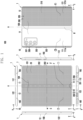
- the electronic device (or foldable electronic device) 1 may include a foldable housing 10 and a flexible display (or, a flexible display module, a bendable display, or a bendable display module) 20.
- the foldable housing 10 may have a front surface 10A of the electronic device 1 and a rear surface 10B of the electronic device 1 opposite to the front surface 10A.
- the front surface 10A of the electronic device 1 is interpreted as a surface where the flexible display 20 is exposed to the outside, and the rear surface 10B of the electronic device 1 is interpreted as a surface located opposite to the front surface 10A.
- the foldable housing 10 may have a first side surface 10C and a second side surface 10D of the electronic device 1 at least partially surrounding a space between the front surface 10A and the rear surface 10B.
- the front surface 10A may include a first cover area a, a second cover area b, and a folding cover area F between the first cover area a and the second cover area b.
- the front surface 10A In the unfolded state of the foldable housing 10 (or the electronic device 1), the front surface 10A may be substantially planar, and all of the first cover area a, the second cover area b, and the folding cover area F may face substantially in the same direction.
- the rear surface 10B may include a third cover area c and a fourth cover area d.
- the foldable housing 10 may include a front cover (e.g., a window) 101 that provides (or forms) at least in part the front surface 10A.
- the flexible display 20 may be positioned in an internal space of the electronic device 1 while overlapping at least in part with the front cover 101.
- the front cover 101 may protect the flexible display 20 from the outside and may be substantially transparent. Light outputted from the flexible display 20 may pass through the front cover 101 and travel to the outside.
- the front cover 101 may include, for example, a plastic film (e.g., polyimide film) or thin glass (e.g., ultra-thin glass (UTG)).
- the front cover 101 may include a plurality of layers.
- the front cover 101 may have a form (not shown separately) in which a coating layer or protective layer of various polymer materials (e.g., polyester (PET), polyimide (PI), or thermoplastic polyurethane (TPU)) is disposed on a plastic film or a thin glass.
- various polymer materials e.g., polyester (PET), polyimide (PI), or thermoplastic polyurethane (TPU)
- the electronic device 1 may include another display (hereinafter, sub-display) 210 positioned inside the first housing 11 and adjacent to the first rear cover 111. A portion of the first rear cover 111 may overlap with the sub-display 210 and may be substantially transparent. The electronic device 1 may output an image using the sub-display 210 instead of the flexible display 20 in the folded state of FIG. 2 .
- sub-display another display
- the display panel 21 may include a light emitting layer 21a, a thin film transistor (TFT) film 21b, and/or an encapsulation layer (e.g., thin-film encapsulation (TFE)) 21c.
- the light emitting layer 21a may have, for example, a plurality of pixels implemented as light emitting devices such as OLEDs or micro LEDs.
- the light emitting layer 21a may be disposed on the TFT film 21b through organic material evaporation.
- the TFT film 21b may be positioned between the light emitting layer 21a and the base film 22.
- the display panel 21 may include a storage capacitor, and the storage capacitor may maintain a voltage signal in the pixel, maintain a voltage applied to the pixel within one frame, or reduce a change in a gate voltage of the TFT due to a leakage current during a light emission time.
- the storage capacitor may maintain the voltage applied to the pixel at a predetermined time interval.
- the touch sensing circuit may be disposed between the front cover 101 and the optical layer 24 (e.g., add-on type).
- the flexible display 20 may include a conductive pattern (not shown) such as a metal mesh (e.g., aluminum mesh) as a touch sensing circuit disposed on the encapsulation layer 21c between the encapsulation layer 21c and the optical layer 24.
- a metal mesh e.g., aluminum mesh
- the metal mesh may have greater durability than a transparent conductive layer implemented with ITO.
- a plurality of layers included in the display panel 21 or the lower panel 23, a stacking structure thereof, or a stacking order may vary.
- the flexible display 20 may be implemented by omitting some of the above components or adding other components according to its provision form or convergence trend.
- an electromagnetic induction panel (e.g., a digitizer) 501 may be positioned between the buffer layer 23b and the lower layer 23c.
- the electromagnetic induction panel 501 may be positioned between the composite sheet 23d and the conductive sheet 23e of the lower layer 23c.
- the electromagnetic induction panel 501 may be positioned between the light blocking layer 23a and the buffer layer 23b.
- the electromagnetic induction panel 501 may be implemented in a form such as a flexible film or a flexible sheet.
- the electromagnetic induction panel 501 may be provided (or formed) as, for example, a flexible printed circuit board.
- an electromagnetic field may be formed by a plurality of electrode patterns included in the electromagnetic induction panel 501.
- the pen input device may be implemented with an electromagnetic induction scheme (e.g., an electro-magnetic resonance (EMR) scheme).
- EMR electro-magnetic resonance
- the pen input device may include a resonance circuit, and the resonance circuit may be interlocked with the electromagnetic induction panel 501.
- a current may flow through the coil included in the resonance circuit of the pen input device by electromagnetic induction.
- the pen input device generates a signal (e.g., a radio frequency signal) (e.g., a position signal, a pen pressure signal, and/or an angle signal) related to a user input on the screen by using the energy supplied from the electromagnetic induction panel 501 and transmit it to the screen (e.g., the electromagnetic induction panel 501).
- a signal e.g., a radio frequency signal
- a position signal e.g., a position signal, a pen pressure signal, and/or an angle signal
- the electromagnetic induction panel 501 may be defined or interpreted as a component included in the flexible display 20.
- the pen input device may be implemented with an active electrical stylus (AES) scheme or an electric coupled resonance (ECR) scheme. In this case, the electromagnetic induction panel 501 may be omitted.
- AES active electrical stylus
- ECR electric coupled resonance
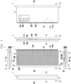
- the support sheet 502 may include a lattice structure (not shown separately) provided (or formed) in a portion corresponding to the folding cover area F of the front cover 101.
- the lattice structure may have, for example, a plurality of openings (or slits).
- the plurality of openings may be periodically provided (or formed) and repeatedly arranged at regular intervals while having substantially the same shape.
- the lattice structure including the plurality of openings may be referred to as an ⁇ opening pattern'.
- the lattice structure may contribute to flexibility for a portion of the display assembly 30 corresponding to the folding cover area F.
- the support sheet 502 may include a recess pattern (not shown) having a plurality of recesses, replacing the lattice structure.
- the lattice structure or recess pattern contributing to the flexibility of the flexible display 20 may be further extended to the other portion.
- the support sheet 502 including the lattice structure or recess pattern, or a corresponding conductive member may be provided (or formed) as a plurality of layers.
- the support sheet 502 may be omitted or may be defined or interpreted as a component included in the flexible display 20.
- the plurality of recesses 601 may be arranged based on the fourth pitch P4 in a direction (e.g., in the x-axis direction) substantially perpendicular to the folding axis A.
- the fourth pattern 40 of the first layer 310 is not limited to the illustrated example and may vary.
- the fourth pattern 40 may be modified to have a first sub-pattern in which first openings or first recesses of a first shape are arranged at a pitch of a first value in a first direction, and a second sub-pattern in which second openings or second recesses different from the first shape are arranged at a pitch of the first value or a second value different from the first value in a second direction different from the first direction.
- the fourth pattern 40 may be modified in a form in which the same shaped openings or recesses are arranged at the same or different pitches in at least two or more directions (e.g., directions perpendicular to each other).
- the shape of the fourth pattern 40 may be provided (or formed) in various ways to secure the flexibility of the first layer 310.
- the fourth pattern 40 of the first layer 310 may be provided (or formed) to reduce a moire phenomenon when light is outputted from a plurality of sub-pixels included in the display panel 21.
- the moire phenomenon may be a phenomenon that, when light is outputted from a plurality of sub-pixels included in the display panel 21, the fourth pattern 40 of the first layer 310 causes light interference, and thus a certain pattern (e.g., a moire pattern) is visually recognized.
- the plurality of sub-pixels may include, for example, a plurality of first sub-pixels outputting light of a first color among three primary colors, a plurality of second sub-pixels outputting light of a second color among three primary colors, and a plurality of third sub-pixels outputting light of a third color among the three primary colors.
- the plurality of first sub-pixels may provide (or form) a first pattern arranged at a first pitch (or first interval) in substantially the same direction as a direction in which the plurality of openings 401 or the plurality of recesses 601 included in the fourth pattern 40 of the first layer 310 are arranged at the fourth pitch P4.
- the plurality of second sub-pixels may provide (or form) a second pattern arranged at a second pitch (or second interval) in substantially the same direction as a direction in which the plurality of openings 401 or the plurality of recesses 601 included in the fourth pattern 40 of the first layer 310 are arranged at the fourth pitch P4.
- the plurality of third sub-pixels may provide (or form) a third pattern arranged at a third pitch (or third interval) in substantially the same direction as a direction in which the plurality of openings 401 or the plurality of recesses 601 included in the fourth pattern 40 of the first layer 310 are arranged at the fourth pitch P4.
- a spatial frequency vector provided (or formed) through convolution summation of a fourth spatial frequency vector provided (or formed) due to the fourth pitch P4 of the fourth pattern 40 included in the first layer 310 and a first spatial frequency vector provided (or formed) due to the first pitch of the first pattern for the plurality of first sub-pixels may be located within a visibility circle with respect to approximately 60 cycles/degree corresponding to the limit pitch that can be perceived by a person, and thus the moire phenomenon may not occur substantially.
- a spatial frequency vector provided (or formed) through convolution summation of a fourth spatial frequency vector provided (or formed) due to the fourth pitch P4 of the fourth pattern 40 included in the first layer 310 and a second spatial frequency vector provided (or formed) due to the second pitch of the second pattern for the plurality of second sub-pixels may be located within a visibility circle with respect to approximately 60 cycles/degree corresponding to the limit pitch that can be perceived by a person, and thus the moire phenomenon may not occur substantially.
- a spatial frequency vector provided (or formed) through convolution summation of a fourth spatial frequency vector provided (or formed) due to the fourth pitch P4 of the fourth pattern 40 included in the first layer 310 and a third spatial frequency vector provided (or formed) due to the third pitch of the third pattern for the plurality of third sub-pixels may be located within a visibility circle with respect to approximately 60 cycles/degree corresponding to the limit pitch that can be perceived by a person, and thus the moire phenomenon may not occur substantially.
- FIG. 7 is a cross-sectional view 700 (e.g., a cross-sectional view or structure in the x-z plane) of a display assembly 70 included in the electronic device 1 taken along line C-C' in FIG. 1 , according to various embodiments.
- a cross-sectional view 700 e.g., a cross-sectional view or structure in the x-z plane
- the second layer 320 may not include a portion disposed (e.g., filled) in the plurality of openings 401 of the first layer 310.
- the display assembly 30 may include a material disposed (e.g., filled) in the plurality of openings 401 of the first layer 310.
- the material disposed (e.g., filled) in the plurality of openings 401 may be substantially transparent.
- a material e.g., a flexible polymer material that does not deteriorate the flexibility of the first layer 310 may be disposed (e.g., filled).
- the material disposed (e.g., filled) in the plurality of openings 401 may reinforce the first layer 310. Impact resistance or durability of the first layer 310 may be reinforced by the material disposed (e.g., filled) in the plurality of openings 401.
- the material disposed (e.g., filled) in the plurality of openings 401 may relieve bending stress occurring in a bent area of the first layer 310 corresponding to the folding cover area F of the front cover 101 in the folded state (see FIG. 2 ) of the electronic device 1.
- the material disposed (e.g., filled) in the plurality of openings 401 may relieve the bending stress generated in the first layer 310.
- the material disposed (e.g., filled) in the plurality of openings 401 of the first layer 310 may be a material capable of reducing light loss by reducing a difference in refractive index with a material included in the first layer 310, a difference in refractive index with the second layer 320, and/or a difference in refractive index with the third layer 330.
- the material disposed (e.g., filled) in the plurality of openings 401 may be different from a material included in the second layer 320. In some embodiments, the material disposed (e.g., filled) in the plurality of openings 401 may be the same as a material included in the second layer 320.
- FIG. 8 is a cross-sectional view 800 (e.g., a cross-sectional view or structure in the x-z plane) of a display assembly 30 in which the second layer 320 of the FIG. 7 embodiment is modified, according to various embodiments.
- a cross-sectional view 800 e.g., a cross-sectional view or structure in the x-z plane
- the display assembly 30 may include a material disposed (e.g., filled) in the plurality of openings 401.
- the material disposed (e.g., filled) in the plurality of openings 401 may be substantially transparent.
- a material e.g., a flexible polymer material
- the material disposed (e.g., filled) in the plurality of openings 401 may reinforce the first layer 310. Impact resistance or durability of the first layer 310 may be reinforced by the material disposed (e.g., filled) in the plurality of openings 401.
- the material disposed (e.g., filled) in the plurality of openings 401 may relieve bending stress occurring in a bent area of the first layer 310 corresponding to the folding cover area F of the front cover 101 in the folded state (see FIG. 2 ) of the electronic device 1. Because the bending stress occurring in the first layer 310 due to a repeated change between the unfolded state and the folded state of the electronic device 1 may cause a decrease or loss of elastic force due to fatigue accumulation and thereby result in breakage, the material disposed (e.g., filled) in the plurality of openings 401 may relieve the bending stress generated in the first layer 310.
- the material disposed (e.g., filled) in the plurality of openings 401 of the first layer 310 may be a material capable of reducing light loss by reducing a difference in refractive index with a material included in the first layer 310, a difference in refractive index with the second layer 320, a difference in refractive index with the third layer 330, and/or a difference in refractive index with a fifth layer 350.
- the material disposed (e.g., filled) in the plurality of openings 401 may be different from a material included in the second layer 320. In some embodiments, the material disposed (e.g., filled) in the plurality of openings 401 may be the same as a material included in the second layer 320.
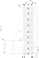
- FIG. 9 is a diagram (e.g., the x-y plan view) illustrating a positional relationship between a lattice structure included in a front cover 101 and a plurality of sub-pixels 900 included in a flexible display 20 in an unfolded state of an electronic device 1, according to an embodiment.
- FIG. 10 is an enlarged view of a portion indicated by reference numeral '901' in FIG. 9 , according to an embodiment.
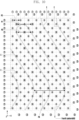
- the plurality of sub-pixels 900 may include red sub-pixels R outputting red light (or expressing a red color), green sub-pixels G outputting green light (or expressing a green color), and blue sub-pixels B outputting blue light (or expressing a blue color).
- the plurality of sub-pixels 900 may be included in, for example, the light emitting layer 21a (see FIG. 5 ) of the display panel 21.
- one pixel (or unit pixel) may be implemented with three sub-pixels, for example, a red sub-pixel R, a green sub-pixel G, and a blue sub-pixel B.
- the arrangement of the plurality of sub-pixels 900 may be implemented differently from the illustrated example.
- one pixel may be implemented with two sub-pixels, for example, a red sub-pixel R and a green sub-pixel G, or a blue sub-pixel B and a green sub-pixel G, and the arrangement of the plurality of sub-pixels 900 may be modified differently from the illustrated example.
- the light outputted from the red sub-pixel R, the light outputted from the green sub-pixel G, and the light outputted from the blue sub-pixel B may have different wavelengths.
- the red sub-pixels R may provide (or form) a first pattern arranged at a first pitch (or first interval) P1 in substantially the same direction as a direction in which the plurality of openings 401 (see FIG. 3 , 7 , or 8 ) or the plurality of recesses 601 (see FIG. 6 ) included in the fourth pattern 40 of the first layer 310 are arranged at the fourth pitch (or fourth interval) P4.
- the green sub-pixels G may provide (or form) a second pattern arranged at a second pitch (or second interval) P2 in substantially the same direction as a direction in which the plurality of openings 401 or the plurality of recesses 601 included in the fourth pattern 40 of the first layer 310 are arranged at the fourth pitch P4.
- the blue sub-pixels B may provide (or form) a third pattern arranged at a third pitch (or third interval) P3 in substantially the same direction as a direction in which the plurality of openings 401 or the plurality of recesses 601 included in the fourth pattern 40 of the first layer 310 are arranged at the fourth pitch P4.
- the first pitch P1, the second pitch P2, or the third pitch P3 may be, but is not limited to, about 30 ⁇ m to about 300 ⁇ m.
- a spatial frequency vector provided (or formed) through convolution summation of a fourth spatial frequency vector provided (or formed) due to the fourth pitch P4 of the fourth pattern 40 included in the first layer 310 and a first spatial frequency vector provided (or formed) due to the first pitch P1 of the first pattern for the red sub-pixels R may be located within a visibility circle with respect to about 60 cycles/degree corresponding to the limit pitch that can be perceived by a person, and thus the moire phenomenon may not occur substantially.
- the fourth pitch P4 is formed to be greater than the first pitch P1, so that the moire phenomenon may be reduced.
- a spatial frequency vector provided (or formed) through convolution summation of a fourth spatial frequency vector provided (or formed) due to the fourth pitch P4 of the fourth pattern 40 included in the first layer 310 and a second spatial frequency vector provided (or formed) due to the second pitch P2 of the second pattern for the green sub-pixels G may be located within a visibility circle with respect to about 60 cycles/degree corresponding to the limit pitch that can be perceived by a person, and thus the moire phenomenon may not occur substantially.
- the fourth pitch P4 is formed to be greater than the second pitch P2, so that the moire phenomenon may be reduced.
- the second pitch P2 may be formed to have a value corresponding to about 0.01 to about 0.8 compared to the fourth pitch P4, based on a spatial frequency vector based on the Fourier transform, thereby reducing the moire phenomenon.
- the ratio of the second pitch P2 to the fourth pitch P4 may not be limited to the above value.
- a spatial frequency vector provided (or formed) through convolution summation of a fourth spatial frequency vector provided (or formed) due to the fourth pitch P4 of the fourth pattern 40 included in the first layer 310 and a third spatial frequency vector provided (or formed) due to the third pitch P3 of the third pattern for the blue sub-pixels B may be located within a visibility circle with respect to about 60 cycles/degree corresponding to the limit pitch that can be perceived by a person, and thus the moire phenomenon may not occur substantially.
- the fourth pitch P4 is formed to be greater than the third pitch P3, so that the moire phenomenon may be reduced.
- the third pitch P3 may be formed to have a value corresponding to about 0.01 to about 0.8 compared to the fourth pitch P4, based on a spatial frequency vector based on the Fourier transform, thereby reducing the moire phenomenon.
- the ratio of the third pitch P3 to the fourth pitch P4 may not be limited to the above value.
- the plurality of openings 401 (see FIG. 3 ) or the plurality of recesses 601 included in the fourth pattern 40 of the first layer 310 may have edges E.
- the edge E of the fourth pattern 40 may indicate (or be defined or interpreted as) an edge shape of the plurality of openings 401 or the plurality of recesses 601 in a direction substantially parallel to the display panel 21 (see FIG. 5 ) including the plurality of sub-pixels 900.
- the edge E of the fourth pattern 40 may correspond to a surface (e.g., an inner surface) included in the plurality of openings 401 while being substantially perpendicular to the third surface 303 or the fourth surface 304.
- the first layer 310 may be provided (or formed) as a thin film having a thickness of, for example, about 30 ⁇ m to about 1000 ⁇ m, and the surface included in the plurality of openings 401 may be interpreted as having an insignificant height compared to the width of the plurality of openings 401. In some embodiments, various other terms may be used to replace the term ⁇ edge'.
- an arrangement direction may be defined with respect to the red sub-pixels R, the green sub-pixels G, or the blue sub-pixels B in the plurality of sub-pixels 900.
- the arrangement direction with respect to the plurality of sub-pixels 900 may be defined, for example, based on a combination of two sub-pixels that output light of the same wavelength (or same color) and are located adjacent to each other at a distance that can substantially affect each other (e.g., interference of light).
- the arrangement directions of the red sub-pixels emitting light of a first wavelength of red color, the green sub-pixels emitting light of a second wavelength of green color, and the blue sub-pixels emitting light of a third wavelength of blue color may include, as shown, a first arrangement direction 1, a second arrangement direction (2), a third arrangement direction (3), and/or a fourth arrangement direction 4.
- the edge E of the fourth pattern 40 included in the first layer 310 may be provided (or formed) so as not to be substantially parallel to the first arrangement direction 1, the second arrangement direction (2), the third arrangement direction 3, and the fourth arrangement direction 4 with respect to the plurality of sub-pixels 900.
- the edge E of the fourth pattern 40 may be provided (or formed) so as not to be parallel to the first arrangement direction 1, the second arrangement direction (2), the third arrangement direction 3, and the fourth arrangement direction 4.
- the edge E of the fourth pattern 40 may have at least one straight section (or straight line shape), and the at least one straight section of the edge E may not be substantially parallel to the first arrangement direction 1, the second arrangement direction 2, the third arrangement direction 3, and the fourth arrangement direction 40.
- the at least one straight section of the edge E may form an angle within a range corresponding to a level of preventing or reducing (e.g., minimizing) the moire phenomenon with the first arrangement direction 1, the second arrangement direction (2), the third arrangement direction 3, or the fourth arrangement direction 4.
- the above range may about 3 degrees or more from each axis of the first arrangement direction, the second arrangement direction, the third arrangement direction, and the fourth arrangement direction. In some embodiments, the range may not be limited to the above angle.
- FIG. 11 is a diagram (e.g., the x-y plan view) illustrating a first layer 310 including a fourth pattern, according to various embodiments.
- the plurality of red sub-pixels, the plurality of green sub-pixels, or the plurality of blue sub-pixels included in the display panel 21 may be arranged to provide (or form) a pattern at a pitch smaller than the fifth pitch P5 in substantially the same direction as a direction in which the plurality of openings 1101 included in the first sub-pattern of the first layer 310 are arranged at the fifth pitch P5.
- the edges of the plurality of openings 1101 may be provided (or formed) so as not to be substantially parallel to the arrangement directions (e.g., the first arrangement direction 1, the second arrangement direction (2), the third arrangement direction 3, and the fourth arrangement direction 4 in FIG. 8 ) regarding the plurality of sub-pixels included in the display panel 21.
- the plurality of red sub-pixels, the plurality of green sub-pixels, or the plurality of blue sub-pixels included in the display panel 21 may be arranged to provide (or form) a pattern at a pitch smaller than the eighth pitch P8 in substantially the same direction as a direction in which the plurality of second openings 1202 included in the second sub-pattern of the first layer 310 are arranged at the eighth pitch P8.
- a load may be applied or transferred from the outside to the front cover 101 (e.g., the window or the front plate) for various reasons.
- a load or pressure load
- a load may be applied or transferred to the front cover 101 due to the pressure of the pen input device.
- a load e.g., an impact load
- a load may be applied to or transferred to the front cover 101.
- the first plate 1311 may be a surface plate.
- the flexible material e.g., the first layer 310 in FIG. 3 or a stack structure including the first layer 310) to be tested may be disposed on the first plate 1311.
- the first plate 1311 may have a support surface 1311a on which the flexible material to be tested is disposed.
- the support surface 1311a of the first plate 1311 may be substantially planar.
- the first plate 1311 may have an opening 1311b corresponding to the probe 1320.
- the opening 1311b may reduce or prevent the effect of the first plate 1311 on detecting the strength of the flexible material.
- the opening 1311b may prevent the first plate 1311 from interfering with the linear movement of the probe 1320.
- the probe 1320 may include a pen input device (e.g., an electronic pen, a digital pen, or a stylus pen).
- the pen input device may be disposed in the test device 1300 while being erected in a direction substantially perpendicular to the support surface 1311a of the first plate 1311.
- a pen tip 1321 of the pen input device may press the first layer 310 (e.g., thin glass, see FIG. 3 ) disposed on the first plate 1311. It may be understood that, in the test device 1300, what the vertically erected pen input device is moved and applies a load to the first layer 310 (see FIG. 3 ) is at least similar to a situation in which the user misses and drops the pen input device or a situation in which the user performs a touch input with the pen input device.
- the first evaluation and the second evaluation may be substantially performed through the test device 1300 in accordance with the ASTM F1306-16 standard.
- a first protective film 1611 of polymer may be disposed on (e.g., attached to) the third surface 303 of the first layer 310 (e.g., thin glass) through a first adhesive material 1612.
- a second protective film 1621 of polymer may be disposed on (e.g., attached to) the fourth surface 304 of the first layer 310 through a second adhesive material 1622.
- the first protective film 1611 and the second protective film 1621 may be, for example, polyethylene terephthalate (PET) having a thickness of substantially about 50 ⁇ m.
- the first adhesive material 1612 and the second adhesive material 1622 may be, for example, a pressure sensitive adhesive (PSA) having a thickness of substantially about 25 ⁇ m or of 25 ⁇ m or less.
- PSA pressure sensitive adhesive
- a ratio of the second interval (e.g., the first pitch P1, the second pitch P2, or the third pitch P3 in FIG. 10 ) to the first interval (e.g., the fourth pitch P4 in FIG. 3 , 6 , 7 , or 8 ) may be 0.01:1 to 0.8:1.
- an edge shape (e.g., the edge E in FIG. 10 ) of the plurality of openings (e.g., the plurality of openings 401 in FIG. 3 , 7 , or 8 ) or the plurality of recesses (e.g., the plurality of recesses 601 in FIG. 6 ) in at least one direction parallel to the flexible display may be formed (or provided) so as not to be parallel to one or more directions in which the plurality of sub-pixels emitting light of the same wavelength in the flexible display are periodically arranged.
- the edge shape (e.g., the edge E in FIG. 10 ) of the plurality of openings (e.g., the plurality of openings 401 in FIG. 3 , 7 , or 8 ) or the plurality of recesses (e.g., the plurality of recesses 601 in FIG. 6 ) in at least one direction parallel to the flexible display may include a straight section.
- the straight section may form an angle of 3 degrees or more with the one or more directions in which the plurality of sub-pixels emitting light of the same wavelength in the flexible display are periodically arranged.
- the edge shape (e.g., the edge E in FIG. 10 ) of the plurality of openings (e.g., the plurality of openings 401 in FIG. 3 , 7 , or 8 ) or the plurality of recesses (e.g., the plurality of recesses 601 in FIG. 6 ) in at least one direction parallel to the flexible display may further include a straight section or a curved section forming an angle of 3 degrees or more with the one or more directions in which the plurality of sub-pixels emitting light of the same wavelength in the flexible display are periodically arranged.
- the plurality of openings e.g., the plurality of openings 401 in FIG. 3 , 7 , or 8
- the plurality of recesses e.g., the plurality of recesses 601 in FIG. 6
- the plurality of openings e.g., the plurality of openings 401 in FIG. 3 , 7 , or 8
- the plurality of recesses e.g., the plurality of recesses 601 in FIG. 6
- the plurality of sub-pixels may emit red light, green light, or blue light.
- the front cover (e.g., the front cover 101 in FIG. 3 , 6 , 7 , or 8 ) may include a first layer (e.g., the first layer 310 in FIG. 3 , 6 , 7 , or 8 ).
- the first layer may have the pattern (e.g., the pattern 40 in FIG. 4 or 10 ), and may be formed of glass.
- the first layer (e.g., the first layer 310 in FIG. 3 , 6 , 7 , or 8 ) may have a thickness of 30 ⁇ m to 1000 ⁇ m.
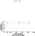
- the first layer (e.g., the first layer 310 in FIG. 3 , 6 , 7 , or 8 ) may have breaking strength of 3 kgf or of 3 kgf or more based on the ASTM F1306-16 standard.
- the first layer (e.g., the first layer 310 in FIG. 3 , 6 , 7 , or 8 ) may have a surface compressive stress of 100 MPa or of 100 MPa or more.
- the electronic device may further include a pen input device.
- the pen input device may have a weight of 5.6 g.
- the pen tip of the pen input device may have a diameter of 0.3 mm.
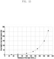
- the first layer may have a strength not to be broken when the drop height of the pen input device is 6 cm or is 6 cm or more.
- the electronic device may further include a pen input device.
- the pen input device may have a weight of 5.6 g.
- the pen tip of the pen input device may have a diameter of 0.3 mm.
- the first layer e.g., the first layer 310 in FIG. 3 , 6 , 7 , or 8
- the first layer may have a strength not to be broken against a pressure load of 0.3 kgf or of 0.3 kgf or more.
- the first layer (e.g., the first layer 310 in FIG. 3 , 6 , 7 , or 8 ) may be bent without breaking with a radius of curvature of 5 mm or between 0 mm and 5 mm.
- the front cover may further include a second layer (e.g., the second layer 320 in FIG. 3 or 6 ).
- the second layer may be positioned between the first layer and the flexible display.
- the second layer may include polymer, and may have a portion disposed (e.g., filled) in the plurality of openings (e.g., the plurality of openings 401 in FIG. 3 ) or the plurality of recesses (e.g., the plurality of recesses 601 in FIG. 6 ).
- the front cover (e.g., the front cover 101 in FIG. 3 , 6 , 7 , or 8 ) may further include a third layer (e.g., the third layer 330 in FIG. 3 , 6 , 7 , or 8 ) of polymer positioned between the front surface (e.g., the front surface 10A in FIG. 1 or the first layer 301 in FIG. 3 , 6 , 7 , or 8 ) of the electronic device and the first layer (e.g., the first layer 310 in FIG. 3 , 6 , 7 , or 8 ).
- a third layer e.g., the third layer 330 in FIG. 3 , 6 , 7 , or 8
- the front surface e.g., the front surface 10A in FIG. 1 or the first layer 301 in FIG. 3 , 6 , 7 , or 8
- the first layer e.g., the first layer 310 in FIG. 3 , 6 , 7 , or 8
- the electronic device may further include an optically transparent adhesive member (e.g., the optically transparent adhesive member 350 in FIG. 3 , 6 , 7 , or 8 ) positioned between the second layer (e.g., the second layer 320 in FIG. 3 , 6 , 7 , or 8 ) and the flexible display (e.g., the flexible display 20 in FIG. 3 , 6 , 7 , or 8 ).
- an optically transparent adhesive member e.g., the optically transparent adhesive member 350 in FIG. 3 , 6 , 7 , or 8
- the second layer e.g., the second layer 320 in FIG. 3 , 6 , 7 , or 8
- the flexible display e.g., the flexible display 20 in FIG. 3 , 6 , 7 , or 8 .
- the foldable housing (e.g., the foldable housing 10 in FIG. 1 ) may allow the front surface (e.g., the front surface 10A in FIG. 1 ) of the electronic device to be foldable inward based on a folding axis (e.g., the folding axis A in FIG. 1 ).
- the foldable housing (e.g., the foldable housing 10 in FIG. 1 ) may allow the front surface (e.g., the front surface 10A in FIG. 1 ) of the electronic device to be foldable outward based on a folding axis (e.g., the folding axis A in FIG. 1 ).
Landscapes
- Engineering & Computer Science (AREA)
- Theoretical Computer Science (AREA)
- Computer Hardware Design (AREA)
- Physics & Mathematics (AREA)
- General Physics & Mathematics (AREA)
- Microelectronics & Electronic Packaging (AREA)
- Human Computer Interaction (AREA)
- General Engineering & Computer Science (AREA)
- Devices For Indicating Variable Information By Combining Individual Elements (AREA)
- Telephone Set Structure (AREA)
Priority Applications (1)
| Application Number | Priority Date | Filing Date | Title |
|---|---|---|---|
| EP25219971.6A EP4714647A3 (de) | 2021-10-05 | 2022-10-05 | Elektronische vorrichtung mit flexibler anzeige |
Applications Claiming Priority (4)
| Application Number | Priority Date | Filing Date | Title |
|---|---|---|---|
| KR20210131870 | 2021-10-05 | ||
| KR1020220013740A KR20230048999A (ko) | 2021-10-05 | 2022-01-28 | 플렉서블 디스플레이를 포함하는 전자 장치 |
| KR1020220125745A KR20230049030A (ko) | 2021-10-05 | 2022-09-30 | 플렉서블 디스플레이를 포함하는 전자 장치 |
| PCT/KR2022/014998 WO2023059065A1 (ko) | 2021-10-05 | 2022-10-05 | 플렉서블 디스플레이를 포함하는 전자 장치 |
Related Child Applications (1)
| Application Number | Title | Priority Date | Filing Date |
|---|---|---|---|
| EP25219971.6A Division EP4714647A3 (de) | 2021-10-05 | 2022-10-05 | Elektronische vorrichtung mit flexibler anzeige |
Publications (4)
| Publication Number | Publication Date |
|---|---|
| EP4394545A1 true EP4394545A1 (de) | 2024-07-03 |
| EP4394545A4 EP4394545A4 (de) | 2025-01-01 |
| EP4394545C0 EP4394545C0 (de) | 2025-12-03 |
| EP4394545B1 EP4394545B1 (de) | 2025-12-03 |
Family
ID=85803571
Family Applications (2)
| Application Number | Title | Priority Date | Filing Date |
|---|---|---|---|
| EP22878886.5A Active EP4394545B1 (de) | 2021-10-05 | 2022-10-05 | Elektronische vorrichtung mit flexibler anzeige |
| EP25219971.6A Pending EP4714647A3 (de) | 2021-10-05 | 2022-10-05 | Elektronische vorrichtung mit flexibler anzeige |
Family Applications After (1)
| Application Number | Title | Priority Date | Filing Date |
|---|---|---|---|
| EP25219971.6A Pending EP4714647A3 (de) | 2021-10-05 | 2022-10-05 | Elektronische vorrichtung mit flexibler anzeige |
Country Status (3)
| Country | Link |
|---|---|
| US (2) | US12200887B2 (de) |
| EP (2) | EP4394545B1 (de) |
| WO (1) | WO2023059065A1 (de) |
Families Citing this family (1)
| Publication number | Priority date | Publication date | Assignee | Title |
|---|---|---|---|---|
| KR20230116972A (ko) * | 2022-01-28 | 2023-08-07 | 삼성디스플레이 주식회사 | 폴더블 표시 장치 |
Family Cites Families (22)
| Publication number | Priority date | Publication date | Assignee | Title |
|---|---|---|---|---|
| KR101958802B1 (ko) * | 2012-07-26 | 2019-03-18 | 삼성디스플레이 주식회사 | 접이식 표시 장치 |
| KR101482401B1 (ko) | 2013-04-30 | 2015-01-13 | 삼성전기주식회사 | 터치패널을 포함하는 디스플레이장치 및 그 터치패널의 전극패턴 시인성 평가방법 |
| KR102263917B1 (ko) * | 2014-08-06 | 2021-06-11 | 엘지디스플레이 주식회사 | 접이식 디스플레이 장치 |
| CN107250961A (zh) | 2015-02-24 | 2017-10-13 | 夏普株式会社 | 具有触控传感器的显示装置 |
| KR102423407B1 (ko) * | 2015-08-19 | 2022-07-21 | 엘지디스플레이 주식회사 | 폴더블 표시장치용 커버 윈도우 및 이를 포함하는 폴더블 표시장치 |
| KR102366516B1 (ko) * | 2015-08-31 | 2022-02-22 | 엘지디스플레이 주식회사 | 접이식 디스플레이 장치 |
| KR102608263B1 (ko) * | 2016-08-10 | 2023-12-04 | 삼성디스플레이 주식회사 | 윈도우 기판 및 이를 포함하는 표시 장치 |
| CN108254934B (zh) | 2016-12-29 | 2020-07-07 | 南京瀚宇彩欣科技有限责任公司 | 显示装置 |
| CN109427251B (zh) * | 2017-08-31 | 2021-08-10 | 昆山国显光电有限公司 | 一种覆盖膜及柔性显示装置 |
| KR102452606B1 (ko) * | 2017-09-19 | 2022-10-07 | 삼성전자주식회사 | 모아레 시인 방지용 패턴 구조체 및 이를 이용한 디스플레이 장치 |
| KR102403713B1 (ko) * | 2017-10-31 | 2022-05-30 | 엘지디스플레이 주식회사 | 플렉서블 디스플레이 |
| KR20190127074A (ko) * | 2018-05-03 | 2019-11-13 | 삼성전자주식회사 | 폴더블 하우징 및 플렉서블 디스플레이를 포함하는 전자 장치 |
| KR102872943B1 (ko) | 2019-06-11 | 2025-10-20 | 삼성디스플레이 주식회사 | 표시 장치 |
| KR102773861B1 (ko) | 2019-10-08 | 2025-02-28 | 삼성디스플레이 주식회사 | 표시 장치 및 이의 제조 방법 |
| KR102827526B1 (ko) | 2019-10-22 | 2025-06-30 | 엘지디스플레이 주식회사 | 폴더블 디스플레이 장치 |
| KR102146730B1 (ko) * | 2019-12-23 | 2020-08-24 | (주)유티아이 | 플렉시블 커버 윈도우 |
| US11048295B1 (en) * | 2020-01-10 | 2021-06-29 | Sharp Kabushiki Kaisha | Flexible window for foldable display |
| KR102778739B1 (ko) * | 2020-01-17 | 2025-03-12 | 삼성디스플레이 주식회사 | 표시 장치 및 휴대용 단말기 |
| KR20210116774A (ko) | 2020-03-13 | 2021-09-28 | 주식회사 비에스피 | 폴더블 디스플레이 장치 |
| KR102718113B1 (ko) | 2020-03-18 | 2024-10-16 | 주식회사 아모그린텍 | 폴딩 플레이트 및 그 제조방법 |
| KR102262991B1 (ko) | 2020-06-03 | 2021-06-09 | 삼성전자 주식회사 | 슬라이드 아웃 디스플레이를 포함하는 전자 장치 |
| KR102823767B1 (ko) * | 2020-09-07 | 2025-06-23 | 엘지디스플레이 주식회사 | 표시패널과 이를 이용한 표시장치 |
-
2022
- 2022-10-05 EP EP22878886.5A patent/EP4394545B1/de active Active
- 2022-10-05 WO PCT/KR2022/014998 patent/WO2023059065A1/ko not_active Ceased
- 2022-10-05 EP EP25219971.6A patent/EP4714647A3/de active Pending
-
2023
- 2023-01-17 US US18/155,355 patent/US12200887B2/en active Active
-
2025
- 2025-01-09 US US19/014,970 patent/US20250151220A1/en active Pending
Also Published As
| Publication number | Publication date |
|---|---|
| EP4394545C0 (de) | 2025-12-03 |
| WO2023059065A1 (ko) | 2023-04-13 |
| EP4394545B1 (de) | 2025-12-03 |
| EP4394545A4 (de) | 2025-01-01 |
| EP4714647A2 (de) | 2026-03-25 |
| US20230156947A1 (en) | 2023-05-18 |
| US12200887B2 (en) | 2025-01-14 |
| EP4714647A3 (de) | 2026-04-22 |
| US20250151220A1 (en) | 2025-05-08 |
Similar Documents
| Publication | Publication Date | Title |
|---|---|---|
| KR102753048B1 (ko) | 슬라이드 아웃 디스플레이를 포함하는 전자 장치 | |
| US12581797B2 (en) | Electronic device comprising transparent cover including glass and foldable display coupled thereto | |
| US20240431055A1 (en) | Electronic device with structure to reduce damage to glass | |
| US11836324B2 (en) | Electronic device and driving method thereof | |
| KR102710387B1 (ko) | 방수 구조를 포함하는 전자 장치 | |
| US20230081984A1 (en) | Foldable electronic device including flexible printed circuit board | |
| US12232286B2 (en) | Display module including cushion layer and electronic device including display module | |
| KR102871048B1 (ko) | 차폐 구조 및 방수 구조를 포함하는 플렉서블 디스플레이 모듈 및 이를 포함하는 전자 장치 | |
| JP5909560B2 (ja) | 入力装置、表示装置、および電子機器 | |
| KR20220160218A (ko) | 방수 구조를 포함하는 전자 장치 | |
| KR20230017710A (ko) | 디지타이저 및 그것을 포함하는 전자 장치 | |
| US20250151220A1 (en) | Electronic device including flexible display | |
| KR101373641B1 (ko) | 입력 장치, 표시 장치, 및 휴대 단말 | |
| KR20230040174A (ko) | 연성 인쇄 회로 기판을 포함하는 폴더블 전자 장치 | |
| KR20220099047A (ko) | 글라스의 손상을 줄일 수 있는 전자 장치 | |
| KR20230049030A (ko) | 플렉서블 디스플레이를 포함하는 전자 장치 | |
| KR20240023983A (ko) | 플렉서블 디스플레이를 포함하는 전자 장치 | |
| WO2012124543A1 (ja) | 入力装置、電子機器、および携帯端末 | |
| KR102846589B1 (ko) | 플렉서블 디스플레이 및 디스플레이 지지 구조를 포함하는 전자 장치, 및 디스플레이 지지 구조의 제조 방법 | |
| CN118076935A (zh) | 包括柔性显示器的电子装置 | |
| KR20230048999A (ko) | 플렉서블 디스플레이를 포함하는 전자 장치 | |
| KR20250055367A (ko) | 플렉서블 디스플레이를 포함하는 전자 장치 | |
| US20250165037A1 (en) | Display module and electronic device comprising display module | |
| KR20240081309A (ko) | 폴더블 전자 장치 | |
| KR20260002065A (ko) | 힌지 모듈을 포함하는 전자 장치 |
Legal Events
| Date | Code | Title | Description |
|---|---|---|---|
| STAA | Information on the status of an ep patent application or granted ep patent |
Free format text: STATUS: THE INTERNATIONAL PUBLICATION HAS BEEN MADE |
|
| PUAI | Public reference made under article 153(3) epc to a published international application that has entered the european phase |
Free format text: ORIGINAL CODE: 0009012 |
|
| STAA | Information on the status of an ep patent application or granted ep patent |
Free format text: STATUS: REQUEST FOR EXAMINATION WAS MADE |
|
| 17P | Request for examination filed |
Effective date: 20240328 |
|
| AK | Designated contracting states |
Kind code of ref document: A1 Designated state(s): AL AT BE BG CH CY CZ DE DK EE ES FI FR GB GR HR HU IE IS IT LI LT LU LV MC ME MK MT NL NO PL PT RO RS SE SI SK SM TR |
|
| A4 | Supplementary search report drawn up and despatched |
Effective date: 20241129 |
|
| RIC1 | Information provided on ipc code assigned before grant |
Ipc: B32B 3/26 20060101ALI20241126BHEP Ipc: B32B 27/08 20060101ALI20241126BHEP Ipc: B32B 17/10 20060101ALI20241126BHEP Ipc: G09F 9/30 20060101ALI20241126BHEP Ipc: G06F 1/16 20060101AFI20241126BHEP |
|
| DAV | Request for validation of the european patent (deleted) | ||
| DAX | Request for extension of the european patent (deleted) | ||
| GRAP | Despatch of communication of intention to grant a patent |
Free format text: ORIGINAL CODE: EPIDOSNIGR1 |
|
| STAA | Information on the status of an ep patent application or granted ep patent |
Free format text: STATUS: GRANT OF PATENT IS INTENDED |
|
| INTG | Intention to grant announced |
Effective date: 20250626 |
|
| GRAS | Grant fee paid |
Free format text: ORIGINAL CODE: EPIDOSNIGR3 |
|
| GRAA | (expected) grant |
Free format text: ORIGINAL CODE: 0009210 |
|
| STAA | Information on the status of an ep patent application or granted ep patent |
Free format text: STATUS: THE PATENT HAS BEEN GRANTED |
|
| AK | Designated contracting states |
Kind code of ref document: B1 Designated state(s): AL AT BE BG CH CY CZ DE DK EE ES FI FR GB GR HR HU IE IS IT LI LT LU LV MC ME MK MT NL NO PL PT RO RS SE SI SK SM TR |
|
| REG | Reference to a national code |
Ref country code: CH Ref legal event code: F10 Free format text: ST27 STATUS EVENT CODE: U-0-0-F10-F00 (AS PROVIDED BY THE NATIONAL OFFICE) Effective date: 20251203 Ref country code: GB Ref legal event code: FG4D |
|
| REG | Reference to a national code |
Ref country code: DE Ref legal event code: R096 Ref document number: 602022026347 Country of ref document: DE |
|
| REG | Reference to a national code |
Ref country code: IE Ref legal event code: FG4D |
|
| U01 | Request for unitary effect filed |
Effective date: 20251216 |
|
| U07 | Unitary effect registered |
Designated state(s): AT BE BG DE DK EE FI FR IT LT LU LV MT NL PT RO SE SI Effective date: 20251222 |
|
| PG25 | Lapsed in a contracting state [announced via postgrant information from national office to epo] |
Ref country code: ES Free format text: LAPSE BECAUSE OF FAILURE TO SUBMIT A TRANSLATION OF THE DESCRIPTION OR TO PAY THE FEE WITHIN THE PRESCRIBED TIME-LIMIT Effective date: 20251203 |
|
| PG25 | Lapsed in a contracting state [announced via postgrant information from national office to epo] |
Ref country code: NO Free format text: LAPSE BECAUSE OF FAILURE TO SUBMIT A TRANSLATION OF THE DESCRIPTION OR TO PAY THE FEE WITHIN THE PRESCRIBED TIME-LIMIT Effective date: 20260303 |
|
| PG25 | Lapsed in a contracting state [announced via postgrant information from national office to epo] |
Ref country code: HR Free format text: LAPSE BECAUSE OF FAILURE TO SUBMIT A TRANSLATION OF THE DESCRIPTION OR TO PAY THE FEE WITHIN THE PRESCRIBED TIME-LIMIT Effective date: 20251203 |
|
| PG25 | Lapsed in a contracting state [announced via postgrant information from national office to epo] |
Ref country code: RS Free format text: LAPSE BECAUSE OF FAILURE TO SUBMIT A TRANSLATION OF THE DESCRIPTION OR TO PAY THE FEE WITHIN THE PRESCRIBED TIME-LIMIT Effective date: 20260303 |