EP4394614A2 - Vorrichtung und verfahren zur niedriglatenz-umschaltung - Google Patents
Vorrichtung und verfahren zur niedriglatenz-umschaltung Download PDFInfo
- Publication number
- EP4394614A2 EP4394614A2 EP24175982.8A EP24175982A EP4394614A2 EP 4394614 A2 EP4394614 A2 EP 4394614A2 EP 24175982 A EP24175982 A EP 24175982A EP 4394614 A2 EP4394614 A2 EP 4394614A2
- Authority
- EP
- European Patent Office
- Prior art keywords
- data
- function block
- crosspoint switch
- switch
- filter
- Prior art date
- Legal status (The legal status is an assumption and is not a legal conclusion. Google has not performed a legal analysis and makes no representation as to the accuracy of the status listed.)
- Pending
Links
Images


Classifications
-
- H—ELECTRICITY
- H04—ELECTRIC COMMUNICATION TECHNIQUE
- H04L—TRANSMISSION OF DIGITAL INFORMATION, e.g. TELEGRAPHIC COMMUNICATION
- H04L49/00—Packet switching elements
- H04L49/15—Interconnection of switching modules
-
- H—ELECTRICITY
- H04—ELECTRIC COMMUNICATION TECHNIQUE
- H04L—TRANSMISSION OF DIGITAL INFORMATION, e.g. TELEGRAPHIC COMMUNICATION
- H04L49/00—Packet switching elements
- H04L49/20—Support for services
- H04L49/201—Multicast operation; Broadcast operation
-
- G—PHYSICS
- G06—COMPUTING OR CALCULATING; COUNTING
- G06F—ELECTRIC DIGITAL DATA PROCESSING
- G06F13/00—Interconnection of, or transfer of information or other signals between, memories, input/output devices or central processing units
-
- G—PHYSICS
- G06—COMPUTING OR CALCULATING; COUNTING
- G06F—ELECTRIC DIGITAL DATA PROCESSING
- G06F13/00—Interconnection of, or transfer of information or other signals between, memories, input/output devices or central processing units
- G06F13/10—Program control for peripheral devices
- G06F13/12—Program control for peripheral devices using hardware independent of the central processor, e.g. channel or peripheral processor
-
- G—PHYSICS
- G06—COMPUTING OR CALCULATING; COUNTING
- G06F—ELECTRIC DIGITAL DATA PROCESSING
- G06F13/00—Interconnection of, or transfer of information or other signals between, memories, input/output devices or central processing units
- G06F13/38—Information transfer, e.g. on bus
- G06F13/40—Bus structure
- G06F13/4004—Coupling between buses
- G06F13/4022—Coupling between buses using switching circuits, e.g. switching matrix, connection or expansion network
-
- G—PHYSICS
- G06—COMPUTING OR CALCULATING; COUNTING
- G06F—ELECTRIC DIGITAL DATA PROCESSING
- G06F15/00—Digital computers in general; Data processing equipment in general
- G06F15/16—Combinations of two or more digital computers each having at least an arithmetic unit, a program unit and a register, e.g. for a simultaneous processing of several programs
- G06F15/163—Interprocessor communication
- G06F15/17—Interprocessor communication using an input/output type connection, e.g. channel, I/O port
-
- H—ELECTRICITY
- H04—ELECTRIC COMMUNICATION TECHNIQUE
- H04L—TRANSMISSION OF DIGITAL INFORMATION, e.g. TELEGRAPHIC COMMUNICATION
- H04L12/00—Data switching networks
- H04L12/28—Data switching networks characterised by path configuration, e.g. LAN [Local Area Networks] or WAN [Wide Area Networks]
- H04L12/40—Bus networks
- H04L12/407—Bus networks with decentralised control
- H04L12/413—Bus networks with decentralised control with random access, e.g. carrier-sense multiple-access with collision detection [CSMA-CD]
-
- H—ELECTRICITY
- H04—ELECTRIC COMMUNICATION TECHNIQUE
- H04L—TRANSMISSION OF DIGITAL INFORMATION, e.g. TELEGRAPHIC COMMUNICATION
- H04L45/00—Routing or path finding of packets in data switching networks
- H04L45/74—Address processing for routing
- H04L45/745—Address table lookup; Address filtering
- H04L45/74591—Address table lookup; Address filtering using content-addressable memories [CAM]
-
- H—ELECTRICITY
- H04—ELECTRIC COMMUNICATION TECHNIQUE
- H04L—TRANSMISSION OF DIGITAL INFORMATION, e.g. TELEGRAPHIC COMMUNICATION
- H04L49/00—Packet switching elements
- H04L49/10—Packet switching elements characterised by the switching fabric construction
- H04L49/101—Packet switching elements characterised by the switching fabric construction using crossbar or matrix
-
- H—ELECTRICITY
- H04—ELECTRIC COMMUNICATION TECHNIQUE
- H04L—TRANSMISSION OF DIGITAL INFORMATION, e.g. TELEGRAPHIC COMMUNICATION
- H04L49/00—Packet switching elements
- H04L49/30—Peripheral units, e.g. input or output ports
Definitions
- the present invention relates to network data switching, and in particular to an efficient low latency data switch using a combination of one or more crosspoint switches with one or more logic function devices such as FPGAs or ASICs, to implement desired networking functionality.
- the present invention provides a non-transitory computer readable medium for configuration of a data switch, comprising instructions which, when executed by one or more processors, causes performance of the following:
- the logic function device may comprise a field programmable gate array (FPGA), a suitably configured application-specific integrated circuit (ASIC) such as a suitably configured x86 CPU based processor or a multicore microprocessor having an inbuilt network interface, or a plurality of such devices.
- FPGA field programmable gate array
- ASIC application-specific integrated circuit
- Discussion herein of embodiments utilising an FPGA are to be understood as also being applicable to an ASIC or a suitably configured processor within the scope of the present invention.
- Some embodiments of the present invention may thus effectively involve optimising for improved low latency and/or improved determinism (fewer MAC collisions), through the abandonment of optimising bandwidth usage.
- the broadcast functionality of a crosspoint switch to distribute data to more than one receiver, the aggregate bandwidth possible is reduced and individual hardware elements' data throughput is not necessarily maximised, however the present invention recognises that the parallel processing of those multiple identical data streams has other beneficial effects.
- the present invention thus recognises that many existing switches are designed in order to optimise bandwidth and flexibility of use amongst many use cases, but that this is at the expense of latency and determinism.
- the content-based filtering could involve addressing by reference to the destination or source address from L2, L3 or L4, but could also include protocol based filtering, state-based filtering and deep packet inspection in the case of a firewall, intrusion detection, or extrusion detection system, filtering by invalidation of packets which are to be filtered, or any other logic function which is implemented in the FPGA.
- Using the crosspoint switch to copy the data stream to more than one function block in the FPGA allows multiple functions to be performed on the same data simultaneously within the FPGA.
- a single transceiver of the FPGA may serve as both the receive and transmit for each filter.
- the FPGA may pass data to output ports without address filtering, in embodiments in which another device such as the client device connected to the FPGA output port is instead configured for such address filtering.
- Such embodiments thus employ a 'broadcast and filter' approach to addressing each data packet, in contrast to bandwidth optimised layer 2 lookup approaches.
- the upstream data stream may then be output by a transmitter at a port of the FPGA, and passed to the crosspoint switch for delivery to an external network front panel port, or more generally to a client device which might include a network interface card internal to the switch, for example.
- the FPGA logic may be configured to implement a firewall, a layer 3 or 4 function such as IP addressing, or packet conversion, potentially performed in parallel.
- Some embodiments may further provide for data delivery from local devices to a plurality of remote locations by:
- the crosspoint switch may handle both upstream and downstream data, whereby one of the streams of data is directed by the crosspoint switch to the FPGA whereas the other stream of data is connected directly between crosspoint switch front ports to one or more client devices.
- the FPGA may be configured to implement layer 3 (network layer) routing by providing every transceiver with a dedicated routing table. While being hardware inefficient such embodiments present considerable latency advantages as compared to layer 3 routers using a single routing table used for all routing.
- Embodiments of the invention may provide a separate FPGA, or separate FPGA logic, for each of the upstream and downstream data functions. Such embodiments allow the upstream and/or downstream logic to be physically smaller in the FPGA, permitting fewer pipeline stages to be employed in the FPGA logic and providing reduced latency and routing delays. Ensuring that the logic for the upstream and downstream data components do not share hardware such as transceivers is advantageous in easing routing congestion. Similar considerations apply to peer-to-peer configurations such as use of the data switch for load levelling between processor cores in high performance computing applications.
- the present invention recognises that providing an FPGA provides large resources of logic gates and RAM blocks to implement either simple or complex digital computations, with very fast I/Os and data buses. Because the FPGA's logic function is reconfigurable, each port output can potentially have a different logic function implemented, i.e. a simple filter, a multiplex of a number of input streams, a multiplex-and-filter, or a more traditional layer 2 switch function based on a ternary content addressable memory (TCAM). Moreover, such functions can be updated when required and in a programmable and very timely manner which can be critical for applications with time sensitive reconfiguration requirements such as when handling market trading data.
- TCAM ternary content addressable memory
- Some embodiments of the invention may thus further provide a management computer operable to reprogram logic blocks of the FPGA using the applicable hardware description language or the like, thus permitting rapid remote reconfiguration such as the adjustment of a filter function or hard-coded routing rules within microseconds.
- the management computer may for example comprise a 64 bit x86 processor, preferably remotely accessible such as via the Internet.
- the management computer may deliver instructions to the FPGA via a high speed serial computer expansion bus such as PCI express (PCIe), or via a network link.
- PCIe PCI express
- the filters or other logic functions could in some embodiments be internally automatically configured by actions of the or a FPGA. For example configuration information might be passed, in a low-bandwidth way, between multiplexers, filters or logic function blocks of the FPGA, such as for the purpose of emulating the MAC address learning function in a conventional switch.
- the FPGA may be configured with a plurality of functions, with the desired function being adaptively selected by the crosspoint switch switching data to the FPGA port associated with the desired function.
- Data from the crosspoint may be directed to any suitable logic function provided by the FPGA, including for example simple logic gates such as AND or XOR in simpler communications protocols in which the FPGA can operate at layer 1, or more complex combinatorial functions such as filtering and/or multiplexing.
- the logic functions may use the contents of some packet fields as inputs and then modify the contents of other packet fields, as appropriate, using sequential and combinatorial logic.
- Filtering may in some embodiments be based on any one or more of a field or combination of fields, may utilise a filter compiled dynamically from an expression or program, may involve state based inspection by deep packet inspection, or may comprise a financial market data risk checking gateway.
- the logic function may involve a transformation, such as Layer 3 routing (e.g, in Ethernet/IP transform a MAC address based on IP address information), Layer 4 routing (e.g. in IP/UDP or IP/TCP transform an IP address based on UDP or TCP port information, implementing NAT), a financial market data ticker plant or parser, or an application protocol translator.
- the logic function may effect an arbiter, such as to feed data from many sources and discard duplicates (e.g. for combining lossy but high performance communications links with reliable but slow links).
- the FPGA may be configured to effect time stamping of data in the data stream, thus providing a layer 2 function in the same device as layer 1 functions.
- the FPGA may in some embodiments further be provided with an external high speed serial bus connection to an external connector, to enable connection of the FPGA to larger-scale functions such as large data memories, or large computing capacity.
- Data ports of the crosspoint switch may receive data from any suitable cable including for example copper cables using 10GBASE-T interface type or 1000BASE-T interface type, 100BASE-TX copper, optic fibres using 10GBASE-R/1000BASE-X, direct-attach copper.
- the crosspoint switch may receive data from any suitable pluggable module, such as SFP, SFP+, QSFP, QSFP+, CFP.
- Those modules might allow a connection via direct-attach copper, IGBase-SX, 10GBase-SR, 10GBase-LR, DWDM, or other connectivity standards.
- the crosspoint switch might be connected directly to another device using a connector or printed circuit board.
- the computer code or instructions may reside on a server available for purchase by switch owners or administrators, in order to configure their hardware with new functions facilitated by the computer code or instructions
- the computer code or instructions may comprise source code, FPGA hardware description language (HDL), or instructions in a higher level language which may be compiled into HDL, for example.
- the present invention provides a non-transitory computer readable medium for configuration of a data switch, comprising instructions which, when executed by one or more processors, causes performance of the following:
- the higher layer process may comprise conversion of physical layer data for higher level processing, including detecting physical layer idle patterns and physical layer errors, for example 8B/10B code violations.
- the higher layer function may comprise a counter of data packet statistics for the respective interface.
- the higher layer function may additionally or alternatively comprise a counter of a number of packets, by type (unicast, multicast and broadcast).
- the higher layer function may additionally or alternatively comprise a counter of a number of packets, by protocol (Ethernet, IP, UDP, TCP, HTTP, SSH, SNMP, ARP, etc).
- protocol Ethernet, IP, UDP, TCP, HTTP, SSH, SNMP, ARP, etc.
- the higher layer function may additionally or alternatively comprise the ability to inject an idle pattern, or cause an idle pattern to be transmitted onto the wire.
- the higher layer function may additionally or alternatively comprise the ability to timestamp a packet.
- timestamping in a switch is useful for measuring network latency, and for accurate records that can be used for post examination, testing/modelling/replaying historical network traffic.
- the timestamp information may be added to the packet by increasing the size of the packet (prepend or append the timestamp data).
- timestamp data may be added to each packet by replacing a part of the packet that is used for other information.
- Such embodiments of the fifth to eighth aspects of the invention have the benefit that it is possible to timestamp the packets on a fully saturated link, i.e a link which has no more space on the channel for larger packets.
- One approach that does not impact the size of a packet is to replace the frame check sequence (FCS) field in the Ethernet frame with a 32-bit timestamp value. This might be done only after the FCS is checked and found to be error-free. If the FCS is found to be in error then a special timestamp value can be used in the affected packet. The special timestamp will be one that never occurs for a valid packet.
- FCS frame check sequence
- the 32-bit timestamp might represent the number of nanoseconds from a known reference instant in time that can be interpreted as an absolute unit of time by a separate process that also knows the reference instant.
- the 32-bit timestamp may represent the least significant 32 bits of the absolute time in nanoseconds.
- the Ethernet frame preamble may be partially replaced with a timestamp value.
- the data may be downstream data originating from one or more servers and intended for one or more client devices. Additionally or alternatively, the data may be upstream data originating from one or more client devices and intended for one or more servers. Additionally or alternatively, the data may be peer to peer data such as data being switched between nodes of a high performance computing cluster, or between nodes of a data centre network.
- the higher layer function may additionally or alternatively comprise the ability to inject a packet into an interface MAC (media access controller), with the output of the MAC being passed to the physical layer. That is, in such embodiments user software may communicate a packet to the switch via a management interface, and the higher layer function may involve injecting the packet into either the receive or transmit MAC for a specified interface. The packet will then be transmitted on the wire from an interface.
- the packet may alternatively be created by software or hardware (e.g. FPGA) on the device, i.e. originating on the device instead of being communicated over the management interface.
- Some such embodiments may inject a packet or packets in order to subscribe to multicast on behalf of downstream hosts, for example, in accordance with the Internet Group Management Protocol Version 2 (IGMP) the subject of the Internet Society RFC2236, and/or in accordance with a protocol-independent multicast (PIM) routing protocol, and/or in accordance with a border gateway protocol (BGP), or the like.
- IGMP Internet Group Management Protocol Version 2
- PIM protocol-independent multicast
- BGP border gateway protocol
- subscribing or unsubscribing to a multicast group may comprise injecting IGMP packets for transmission to a neighbouring multicast router to register in a multicast group to receive multicast packets on behalf of downstream clients connected to the ports of the switch of the present invention, thereby obviating the need to have a downstream host perform this function.
- data ports of the switch may receive data from any suitable cable including for example copper cables using 10GBASE-T interface type or 1000BASE-T interface type, 100BASF-TX copper, optic fibres using 10GBASE-R/1000BASE-X, direct-attach copper.
- the switch may receive data from any suitable pluggable module, such as SFP, SFP+, QSFP, QSFP+, CFP.
- Those modules might allow a connection via direct-attach copper, 1GBase-SX, 10GBase-SR, 10GBase-LR, DWDM, or other connectivity standards.
- the switch might be connected directly to another device using a connector or printed circuit board.
- the higher layer function to which the data is copied may be adaptively selected by switching the copied data stream to one of a plurality of outputs of the switch, each of the plurality of outputs being connected to a respective higher layer function.
- Such embodiments permit dynamic selection of which higher layer function or functions is or are applied to the copied data stream.
- the output of the higher layer function may be returned to the crosspoint switch to permit dynamic and configurable switching of the output of the higher layer function to any chosen output of the crosspoint.
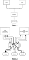
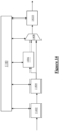
- Figure 1 is a system schematic of the hardware used to implement one embodiment of the present invention. It consists of some front panel ports which can be connected to other devices, some FPGAs which have transceivers which can talk to the front panel ports, and a crosspoint switch which can remap, as well as multicast data from one port to multiple ports. It is noted that not all of the cross point outputs will necessarily be connected to the logic functions of the FPGAs as some ports will be needed to provide data output to external devices.
- upstream component can be implemented in adjacent transceivers with no interaction with the downstream logic, potentially allowing for a much more efficient upstream implementation (e.g. less cycles and lower latency).
- interaction between upstream and downstream logic components may sometimes be required such as when implementing flow control or 1000BASE-X auto negotiation.
Landscapes
- Engineering & Computer Science (AREA)
- Theoretical Computer Science (AREA)
- Computer Networks & Wireless Communication (AREA)
- Signal Processing (AREA)
- Physics & Mathematics (AREA)
- General Engineering & Computer Science (AREA)
- General Physics & Mathematics (AREA)
- Computer Hardware Design (AREA)
- Mathematical Physics (AREA)
- Software Systems (AREA)
- Data Exchanges In Wide-Area Networks (AREA)
- Logic Circuits (AREA)
Applications Claiming Priority (5)
| Application Number | Priority Date | Filing Date | Title |
|---|---|---|---|
| AU2014903158A AU2014903158A0 (en) | 2014-08-13 | Apparatus and Method for Low Latency Switching | |
| AU2014904247A AU2014904247A0 (en) | 2014-10-23 | Apparatus and Method for Low Latency Switching | |
| PCT/AU2014/050391 WO2016023062A1 (en) | 2014-08-13 | 2014-12-03 | Apparatus and method for low latency switching |
| EP19206553.0A EP3641234B1 (de) | 2014-08-13 | 2014-12-03 | Vorrichtung und verfahren zum schalten mit niedriger latenz |
| EP14899656.4A EP3130107B1 (de) | 2014-08-13 | 2014-12-03 | Vorrichtung und verfahren zum schalten mit niedriger latenz |
Related Parent Applications (3)
| Application Number | Title | Priority Date | Filing Date |
|---|---|---|---|
| EP19206553.0A Division-Into EP3641234B1 (de) | 2014-08-13 | 2014-12-03 | Vorrichtung und verfahren zum schalten mit niedriger latenz |
| EP19206553.0A Division EP3641234B1 (de) | 2014-08-13 | 2014-12-03 | Vorrichtung und verfahren zum schalten mit niedriger latenz |
| EP14899656.4A Division EP3130107B1 (de) | 2014-08-13 | 2014-12-03 | Vorrichtung und verfahren zum schalten mit niedriger latenz |
Publications (2)
| Publication Number | Publication Date |
|---|---|
| EP4394614A2 true EP4394614A2 (de) | 2024-07-03 |
| EP4394614A3 EP4394614A3 (de) | 2024-08-28 |
Family
ID=55303681
Family Applications (3)
| Application Number | Title | Priority Date | Filing Date |
|---|---|---|---|
| EP24175982.8A Pending EP4394614A3 (de) | 2014-08-13 | 2014-12-03 | Vorrichtung und verfahren zur niedriglatenz-umschaltung |
| EP19206553.0A Active EP3641234B1 (de) | 2014-08-13 | 2014-12-03 | Vorrichtung und verfahren zum schalten mit niedriger latenz |
| EP14899656.4A Active EP3130107B1 (de) | 2014-08-13 | 2014-12-03 | Vorrichtung und verfahren zum schalten mit niedriger latenz |
Family Applications After (2)
| Application Number | Title | Priority Date | Filing Date |
|---|---|---|---|
| EP19206553.0A Active EP3641234B1 (de) | 2014-08-13 | 2014-12-03 | Vorrichtung und verfahren zum schalten mit niedriger latenz |
| EP14899656.4A Active EP3130107B1 (de) | 2014-08-13 | 2014-12-03 | Vorrichtung und verfahren zum schalten mit niedriger latenz |
Country Status (7)
| Country | Link |
|---|---|
| US (2) | US10630608B2 (de) |
| EP (3) | EP4394614A3 (de) |
| JP (1) | JP2017519449A (de) |
| KR (2) | KR20170042800A (de) |
| AU (1) | AU2014403783B2 (de) |
| CA (1) | CA2946896A1 (de) |
| WO (1) | WO2016023062A1 (de) |
Families Citing this family (21)
| Publication number | Priority date | Publication date | Assignee | Title |
|---|---|---|---|---|
| WO2017197465A1 (en) * | 2016-05-20 | 2017-11-23 | Metamako General Pty Ltd In Its Capacity As General Partner Of Metamako Technology Lp | Systems for transmitting a data stream and methods for transmitting a data stream |
| US11218401B2 (en) * | 2017-08-10 | 2022-01-04 | Arista Networks, Inc. | Computer network device, a computer internetwork and a method for computer networking |
| CN107885694B (zh) * | 2017-10-18 | 2018-10-23 | 广东高云半导体科技股份有限公司 | 一种支持系统级集成电路芯片 |
| US10708127B1 (en) * | 2017-12-29 | 2020-07-07 | Arista Networks, Inc. | Low-latency network switching device with latency identification and diagnostics |
| US10545925B2 (en) | 2018-06-06 | 2020-01-28 | Intel Corporation | Storage appliance for processing of functions as a service (FaaS) |
| US12003608B2 (en) * | 2018-07-12 | 2024-06-04 | Netscout Systems, Inc. | System and method for repurposing layer 2 switch as a layer 1 switch |
| US10387356B1 (en) * | 2018-10-02 | 2019-08-20 | Teradyne, Inc. | Generating timestamps on a packet-oriented bus |
| US12192121B2 (en) | 2019-03-18 | 2025-01-07 | Brightways Corporation | Hyperscale switch element (HSS) for data center network switching |
| US10630606B1 (en) * | 2019-03-18 | 2020-04-21 | Brightways Corporation | System, method and architecture for data center network switching |
| US11652561B2 (en) * | 2019-06-21 | 2023-05-16 | Intel Corporation | Techniques for determining timestamp inaccuracies in a transceiver |
| JP6960011B2 (ja) * | 2020-04-20 | 2021-11-05 | 株式会社インタフェース | Tsn対応エンドコントローラを備えたネットワークシステム |
| CA3161220C (en) | 2021-07-27 | 2025-06-10 | Orthogone Technologies Inc. | LOW LATENCY NETWORK DEVICE AND METHOD FOR PROCESSING SERIALLY RECEIVED DATA |
| US11722435B2 (en) * | 2021-11-18 | 2023-08-08 | United States Of America As Represented By The Secretary Of The Navy | System with layer-one switch for flexible communication interconnections |
| CN114338032B (zh) * | 2021-12-02 | 2022-09-30 | 上海健交科技服务有限责任公司 | 面向深度学习的高精度时间戳安全校验加速方法和装置 |
| EP4480135A1 (de) * | 2022-02-18 | 2024-12-25 | Hirschmann Automation and Control GmbH | Bedingte filterung für zeitdeterministische firewalls |
| CN114884903B (zh) * | 2022-04-29 | 2023-06-02 | 绿盟科技集团股份有限公司 | 数据处理方法、现场可编程门阵列芯片及网络安全设备 |
| EP4383729B1 (de) * | 2022-12-07 | 2025-11-05 | Axis AB | Video-failover-aufzeichnung |
| US20240205171A1 (en) * | 2022-12-15 | 2024-06-20 | The United States Of America, As Represented By The Secretary Of The Navy | Dynamically Reconfigurable Network |
| WO2024167645A1 (en) * | 2023-02-10 | 2024-08-15 | Commscope Technologies Llc | Techniques for diminishing latency in a distributed antenna system |
| US12177132B1 (en) * | 2023-09-26 | 2024-12-24 | Morgan Stanley Services Group Inc. | L1 replicator and switch combination |
| US20250300753A1 (en) * | 2024-03-25 | 2025-09-25 | Arista Networks, Inc. | Timestamping of multilane protocols |
Family Cites Families (20)
| Publication number | Priority date | Publication date | Assignee | Title |
|---|---|---|---|---|
| JP2830750B2 (ja) | 1994-02-24 | 1998-12-02 | 日本電気株式会社 | 画像多地点通信制御装置と画像通信端末および画像通信システム |
| JPH11261622A (ja) * | 1998-03-12 | 1999-09-24 | Sumitomo Electric Ind Ltd | フレーム変換装置 |
| US7068666B2 (en) | 2001-04-27 | 2006-06-27 | The Boeing Company | Method and system for virtual addressing in a communications network |
| US20060013135A1 (en) * | 2004-06-21 | 2006-01-19 | Schmidt Steven G | Flow control in a switch |
| US7224184B1 (en) | 2004-11-05 | 2007-05-29 | Xilinx, Inc. | High bandwidth reconfigurable on-chip network for reconfigurable systems |
| US8797870B2 (en) * | 2006-01-05 | 2014-08-05 | Cisco Technology, Inc. | Method and system for calculation of QOV metrics |
| EP2008494A4 (de) | 2006-04-14 | 2013-01-16 | Brixham Solutions Ltd | Hybride datenumschaltung für effiziente paketverarbeitung |
| US7521961B1 (en) * | 2007-01-23 | 2009-04-21 | Xilinx, Inc. | Method and system for partially reconfigurable switch |
| US7920557B2 (en) * | 2007-02-15 | 2011-04-05 | Harris Corporation | Apparatus and method for soft media processing within a routing switcher |
| JP4847585B2 (ja) | 2007-06-12 | 2011-12-28 | 富士通株式会社 | コンフィグレーション装置 |
| JP5670341B2 (ja) | 2008-11-10 | 2015-02-18 | ゾモジョ・ピーティーワイ・リミテッド | 改良された自動化された取引システム |
| JP5240028B2 (ja) * | 2009-04-10 | 2013-07-17 | ソニー株式会社 | 画像処理装置および画像処理部の制御方法 |
| US20100317374A1 (en) * | 2009-06-11 | 2010-12-16 | Yaron Alpert | Apparatus for and method of managing paging interval access on a mobile station |
| US8537697B2 (en) * | 2010-02-19 | 2013-09-17 | Gigamon Inc. | Packet timing measurement |
| US9160668B2 (en) * | 2010-05-03 | 2015-10-13 | Pluribus Networks Inc. | Servers, switches, and systems with switching module implementing a distributed network operating system |
| JP5487135B2 (ja) * | 2011-02-09 | 2014-05-07 | 株式会社東芝 | 送受信システム及び信号伝送方法 |
| JP2012208975A (ja) * | 2011-03-29 | 2012-10-25 | Renesas Electronics Corp | 半導体装置 |
| JP2013131973A (ja) * | 2011-12-22 | 2013-07-04 | Alaxala Networks Corp | パケット廃棄制御方法、中継装置、パケット処理装置 |
| US8891528B2 (en) * | 2012-06-21 | 2014-11-18 | Breakingpoint Systems, Inc. | Managing the capture of packets in a computing system |
| US9674118B2 (en) * | 2014-03-19 | 2017-06-06 | xCelor LLC | System and method for low-latency network data switching |
-
2014
- 2014-12-03 JP JP2016574895A patent/JP2017519449A/ja active Pending
- 2014-12-03 EP EP24175982.8A patent/EP4394614A3/de active Pending
- 2014-12-03 KR KR1020177009077A patent/KR20170042800A/ko not_active Withdrawn
- 2014-12-03 KR KR1020167031097A patent/KR101748546B1/ko not_active Expired - Fee Related
- 2014-12-03 CA CA2946896A patent/CA2946896A1/en not_active Abandoned
- 2014-12-03 WO PCT/AU2014/050391 patent/WO2016023062A1/en not_active Ceased
- 2014-12-03 AU AU2014403783A patent/AU2014403783B2/en not_active Ceased
- 2014-12-03 US US15/315,708 patent/US10630608B2/en active Active
- 2014-12-03 EP EP19206553.0A patent/EP3641234B1/de active Active
- 2014-12-03 EP EP14899656.4A patent/EP3130107B1/de active Active
-
2020
- 2020-03-16 US US16/820,409 patent/US11228538B2/en active Active
Also Published As
| Publication number | Publication date |
|---|---|
| US10630608B2 (en) | 2020-04-21 |
| EP3130107B1 (de) | 2019-11-06 |
| EP3130107A1 (de) | 2017-02-15 |
| WO2016023062A1 (en) | 2016-02-18 |
| AU2014403783A1 (en) | 2016-10-06 |
| EP3130107A4 (de) | 2017-09-06 |
| US20170111295A1 (en) | 2017-04-20 |
| EP3641234B1 (de) | 2024-06-26 |
| EP4394614A3 (de) | 2024-08-28 |
| KR20160137644A (ko) | 2016-11-30 |
| US20200244595A1 (en) | 2020-07-30 |
| EP3641234C0 (de) | 2024-06-26 |
| AU2014403783B2 (en) | 2019-10-03 |
| KR101748546B1 (ko) | 2017-06-16 |
| US11228538B2 (en) | 2022-01-18 |
| EP3641234A1 (de) | 2020-04-22 |
| JP2017519449A (ja) | 2017-07-13 |
| KR20170042800A (ko) | 2017-04-19 |
| CA2946896A1 (en) | 2016-02-18 |
Similar Documents
| Publication | Publication Date | Title |
|---|---|---|
| US11228538B2 (en) | Apparatus and method for low latency switching | |
| US9172647B2 (en) | Distributed network test system | |
| US8358651B1 (en) | Switch device having a plurality of processing cores | |
| US9401876B2 (en) | Method of data delivery across a network fabric in a router or Ethernet bridge | |
| EP3259888A1 (de) | Erzeugung eines hochpräzisen paketzugs | |
| CN101459607B (zh) | 一种报文发送方法和路由器 | |
| US9619410B1 (en) | Systems and methods for packet switching | |
| CN103236956A (zh) | 一种对通讯设备进行吞吐量测试的方法及交换机 | |
| CN113472697A (zh) | 网络信息传输系统 | |
| Antichi et al. | Enabling open-source high speed network monitoring on NetFPGA | |
| CN116508295A (zh) | 带内边缘到边缘往返时间测量 | |
| CN106230718A (zh) | 基于XilinxFPGA多千兆网合流系统及实现方法 | |
| AU2014101296A4 (en) | Apparatus and Method for Improved Physical Layer Switching | |
| EP2803172A1 (de) | Igmp/mld-übersetzung | |
| US11671281B1 (en) | Handling interface clock rate mismatches between network devices | |
| US20040081096A1 (en) | Method and device for extending usable lengths of fibre channel links | |
| Li et al. | SDN-based switch implementation on network processors | |
| US12598228B2 (en) | System and a method for distributing information | |
| Zabołotny | Optimized Ethernet transmission of acquired data from FPGA to embedded system | |
| Orosz et al. | A NetFPGA-based network monitoring system with multi-layer timestamping: Rnetprobe | |
| Moore et al. | MOVING TOWARDS 10 GbE NETWORK SWITCHES AND RECORDERS | |
| CN107612827A (zh) | 一种提高异地数据中心vxlan网络质量的方法和装置 | |
| US20120254397A1 (en) | Method and System for Frame Discard on Switchover of Traffic Manager Resources | |
| Hildin et al. | Airborne Network Switch With IEEE-1588 Support | |
| Edwards et al. | Can COTS Ethernet Switches Handle Uncompressed Video? |
Legal Events
| Date | Code | Title | Description |
|---|---|---|---|
| PUAI | Public reference made under article 153(3) epc to a published international application that has entered the european phase |
Free format text: ORIGINAL CODE: 0009012 |
|
| STAA | Information on the status of an ep patent application or granted ep patent |
Free format text: STATUS: THE APPLICATION HAS BEEN PUBLISHED |
|
| AC | Divisional application: reference to earlier application |
Ref document number: 3130107 Country of ref document: EP Kind code of ref document: P Ref document number: 3641234 Country of ref document: EP Kind code of ref document: P |
|
| AK | Designated contracting states |
Kind code of ref document: A2 Designated state(s): AL AT BE BG CH CY CZ DE DK EE ES FI FR GB GR HR HU IE IS IT LI LT LU LV MC MK MT NL NO PL PT RO RS SE SI SK SM TR |
|
| REG | Reference to a national code |
Ref country code: DE Ref legal event code: R079 Free format text: PREVIOUS MAIN CLASS: G06F0015163000 Ipc: H04L0012413000 |
|
| PUAL | Search report despatched |
Free format text: ORIGINAL CODE: 0009013 |
|
| AK | Designated contracting states |
Kind code of ref document: A3 Designated state(s): AL AT BE BG CH CY CZ DE DK EE ES FI FR GB GR HR HU IE IS IT LI LT LU LV MC MK MT NL NO PL PT RO RS SE SI SK SM TR |
|
| RIC1 | Information provided on ipc code assigned before grant |
Ipc: G06F 13/40 20060101ALI20240719BHEP Ipc: G06F 13/12 20060101ALI20240719BHEP Ipc: G06F 13/00 20060101ALI20240719BHEP Ipc: G06F 15/17 20060101ALI20240719BHEP Ipc: G06F 15/163 20060101ALI20240719BHEP Ipc: H04L 12/413 20060101AFI20240719BHEP |
|
| STAA | Information on the status of an ep patent application or granted ep patent |
Free format text: STATUS: REQUEST FOR EXAMINATION WAS MADE |
|
| 17P | Request for examination filed |
Effective date: 20250219 |
|
| STAA | Information on the status of an ep patent application or granted ep patent |
Free format text: STATUS: EXAMINATION IS IN PROGRESS |
|
| 17Q | First examination report despatched |
Effective date: 20250903 |
|
| GRAP | Despatch of communication of intention to grant a patent |
Free format text: ORIGINAL CODE: EPIDOSNIGR1 |
|
| STAA | Information on the status of an ep patent application or granted ep patent |
Free format text: STATUS: GRANT OF PATENT IS INTENDED |