EP4394828A2 - Composant électronique multicouche - Google Patents
Composant électronique multicouche Download PDFInfo
- Publication number
- EP4394828A2 EP4394828A2 EP23220004.8A EP23220004A EP4394828A2 EP 4394828 A2 EP4394828 A2 EP 4394828A2 EP 23220004 A EP23220004 A EP 23220004A EP 4394828 A2 EP4394828 A2 EP 4394828A2
- Authority
- EP
- European Patent Office
- Prior art keywords
- region
- moles
- dielectric layer
- manganese
- titanium
- Prior art date
- Legal status (The legal status is an assumption and is not a legal conclusion. Google has not performed a legal analysis and makes no representation as to the accuracy of the status listed.)
- Pending
Links
Images


Classifications
-
- H—ELECTRICITY
- H01—ELECTRIC ELEMENTS
- H01G—CAPACITORS; CAPACITORS, RECTIFIERS, DETECTORS, SWITCHING DEVICES, LIGHT-SENSITIVE OR TEMPERATURE-SENSITIVE DEVICES OF THE ELECTROLYTIC TYPE
- H01G4/00—Fixed capacitors; Processes of their manufacture
- H01G4/002—Details
- H01G4/018—Dielectrics
- H01G4/06—Solid dielectrics
- H01G4/08—Inorganic dielectrics
- H01G4/12—Ceramic dielectrics
- H01G4/1209—Ceramic dielectrics characterised by the ceramic dielectric material
- H01G4/1218—Ceramic dielectrics characterised by the ceramic dielectric material based on titanium oxides or titanates
- H01G4/1227—Ceramic dielectrics characterised by the ceramic dielectric material based on titanium oxides or titanates based on alkaline earth titanates
-
- H—ELECTRICITY
- H01—ELECTRIC ELEMENTS
- H01G—CAPACITORS; CAPACITORS, RECTIFIERS, DETECTORS, SWITCHING DEVICES, LIGHT-SENSITIVE OR TEMPERATURE-SENSITIVE DEVICES OF THE ELECTROLYTIC TYPE
- H01G4/00—Fixed capacitors; Processes of their manufacture
- H01G4/30—Stacked capacitors
-
- B—PERFORMING OPERATIONS; TRANSPORTING
- B32—LAYERED PRODUCTS
- B32B—LAYERED PRODUCTS, i.e. PRODUCTS BUILT-UP OF STRATA OF FLAT OR NON-FLAT, e.g. CELLULAR OR HONEYCOMB, FORM
- B32B18/00—Layered products essentially comprising ceramics, e.g. refractory products
-
- H—ELECTRICITY
- H01—ELECTRIC ELEMENTS
- H01G—CAPACITORS; CAPACITORS, RECTIFIERS, DETECTORS, SWITCHING DEVICES, LIGHT-SENSITIVE OR TEMPERATURE-SENSITIVE DEVICES OF THE ELECTROLYTIC TYPE
- H01G4/00—Fixed capacitors; Processes of their manufacture
- H01G4/002—Details
- H01G4/005—Electrodes
-
- H—ELECTRICITY
- H01—ELECTRIC ELEMENTS
- H01G—CAPACITORS; CAPACITORS, RECTIFIERS, DETECTORS, SWITCHING DEVICES, LIGHT-SENSITIVE OR TEMPERATURE-SENSITIVE DEVICES OF THE ELECTROLYTIC TYPE
- H01G4/00—Fixed capacitors; Processes of their manufacture
- H01G4/002—Details
- H01G4/005—Electrodes
- H01G4/012—Form of non-self-supporting electrodes
-
- H—ELECTRICITY
- H01—ELECTRIC ELEMENTS
- H01G—CAPACITORS; CAPACITORS, RECTIFIERS, DETECTORS, SWITCHING DEVICES, LIGHT-SENSITIVE OR TEMPERATURE-SENSITIVE DEVICES OF THE ELECTROLYTIC TYPE
- H01G4/00—Fixed capacitors; Processes of their manufacture
- H01G4/002—Details
- H01G4/018—Dielectrics
- H01G4/06—Solid dielectrics
- H01G4/08—Inorganic dielectrics
- H01G4/12—Ceramic dielectrics
-
- H—ELECTRICITY
- H01—ELECTRIC ELEMENTS
- H01G—CAPACITORS; CAPACITORS, RECTIFIERS, DETECTORS, SWITCHING DEVICES, LIGHT-SENSITIVE OR TEMPERATURE-SENSITIVE DEVICES OF THE ELECTROLYTIC TYPE
- H01G4/00—Fixed capacitors; Processes of their manufacture
- H01G4/002—Details
- H01G4/018—Dielectrics
- H01G4/06—Solid dielectrics
- H01G4/08—Inorganic dielectrics
- H01G4/12—Ceramic dielectrics
- H01G4/1209—Ceramic dielectrics characterised by the ceramic dielectric material
-
- H—ELECTRICITY
- H01—ELECTRIC ELEMENTS
- H01G—CAPACITORS; CAPACITORS, RECTIFIERS, DETECTORS, SWITCHING DEVICES, LIGHT-SENSITIVE OR TEMPERATURE-SENSITIVE DEVICES OF THE ELECTROLYTIC TYPE
- H01G4/00—Fixed capacitors; Processes of their manufacture
- H01G4/002—Details
- H01G4/228—Terminals
-
- C—CHEMISTRY; METALLURGY
- C04—CEMENTS; CONCRETE; ARTIFICIAL STONE; CERAMICS; REFRACTORIES
- C04B—LIME, MAGNESIA; SLAG; CEMENTS; COMPOSITIONS THEREOF, e.g. MORTARS, CONCRETE OR LIKE BUILDING MATERIALS; ARTIFICIAL STONE; CERAMICS; REFRACTORIES; TREATMENT OF NATURAL STONE
- C04B2237/00—Aspects relating to ceramic laminates or to joining of ceramic articles with other articles by heating
- C04B2237/50—Processing aspects relating to ceramic laminates or to the joining of ceramic articles with other articles by heating
- C04B2237/58—Forming a gradient in composition or in properties across the laminate or the joined articles
-
- C—CHEMISTRY; METALLURGY
- C04—CEMENTS; CONCRETE; ARTIFICIAL STONE; CERAMICS; REFRACTORIES
- C04B—LIME, MAGNESIA; SLAG; CEMENTS; COMPOSITIONS THEREOF, e.g. MORTARS, CONCRETE OR LIKE BUILDING MATERIALS; ARTIFICIAL STONE; CERAMICS; REFRACTORIES; TREATMENT OF NATURAL STONE
- C04B2237/00—Aspects relating to ceramic laminates or to joining of ceramic articles with other articles by heating
- C04B2237/50—Processing aspects relating to ceramic laminates or to the joining of ceramic articles with other articles by heating
- C04B2237/80—Joining the largest surface of one substrate with a smaller surface of the other substrate, e.g. butt joining or forming a T-joint
-
- H—ELECTRICITY
- H01—ELECTRIC ELEMENTS
- H01G—CAPACITORS; CAPACITORS, RECTIFIERS, DETECTORS, SWITCHING DEVICES, LIGHT-SENSITIVE OR TEMPERATURE-SENSITIVE DEVICES OF THE ELECTROLYTIC TYPE
- H01G4/00—Fixed capacitors; Processes of their manufacture
- H01G4/002—Details
- H01G4/005—Electrodes
- H01G4/008—Selection of materials
- H01G4/0085—Fried electrodes
-
- H—ELECTRICITY
- H01—ELECTRIC ELEMENTS
- H01G—CAPACITORS; CAPACITORS, RECTIFIERS, DETECTORS, SWITCHING DEVICES, LIGHT-SENSITIVE OR TEMPERATURE-SENSITIVE DEVICES OF THE ELECTROLYTIC TYPE
- H01G4/00—Fixed capacitors; Processes of their manufacture
- H01G4/002—Details
- H01G4/228—Terminals
- H01G4/232—Terminals electrically connecting two or more layers of a stacked or rolled capacitor
Definitions
- the present disclosure relates to a multilayer electronic component.
- a multilayer ceramic capacitor (MLCC), one of multilayer electronic components, may be a chip-type condenser which is mounted on a printed circuit board of various electronic products, such as an imaging device such as a liquid crystal display (LCD) or a plasma display panel (PDP), a computer, a smartphone or a cellular phone, to charge or discharge electricity therein or therefrom.
- an imaging device such as a liquid crystal display (LCD) or a plasma display panel (PDP), a computer, a smartphone or a cellular phone, to charge or discharge electricity therein or therefrom.
- LCD liquid crystal display
- PDP plasma display panel
- the multilayer ceramic capacitor may include a capacitance formation portion in which internal electrodes overlap each other to form capacitance and a margin portion, which is the other region.
- a step difference between the capacitance formation portion and the margin portion may occur during compression and firing due to a difference in stacking degrees of the internal electrodes, and such a difference may structurally cause a weak portion of the margin portion.
- An aspect of the present disclosure may provide a multilayer electronic component which may suppress deterioration of a break down voltage (BDV) characteristic that occurs in a process of forming a step difference compensation part to solve a step difference between the capacitance formation portion and margin portion thereof.
- BDV break down voltage
- Another aspect of the present disclosure may provide a multilayer electronic component which may suppress deterioration of high-temperature reliability that occurs in the process of forming the step difference compensation part to resolve the step difference between the capacitance formation portion and the margin portion thereof.
- the body may include a capacitance formation portion where the first and second internal electrodes overlap each other in the first direction, and a first margin portion disposed on one side surface or the other side surface of the capacitance formation portion in the second direction and including one end of the first or second internal electrode.
- the dielectric layer may include a first region disposed at a center region of the dielectric layer that is included in the capacitance formation portion, and a second region included in the first margin portion.
- a multilayer electronic component may include: a body having first and second surfaces opposing each other in a first direction, third and fourth surfaces connected to the first and second surfaces and opposing each other in a second direction, and fifth and sixth surfaces connected to the first to fourth surfaces and opposing each other in a third direction, and including a dielectric layer and first and second internal electrodes alternately disposed in the first direction while having the dielectric layer interposed therebetween; a first external electrode disposed on the third surface and connected to the first internal electrode; and a second external electrode disposed on the fourth surface and connected to the second internal electrode.
- the body may include a capacitance formation portion where the first and second internal electrodes overlap each other in the first direction, a first margin portion disposed on one side surface or the other side surface of the capacitance formation portion in the second direction and including an end of the first or second internal electrode, and a second margin portion disposed on one surface or the other surface of the capacitance formation portion in the third direction.
- the dielectric layer may include a first region disposed at a center region of the dielectric layer that is included in the capacitance formation portion, a second region included in the first margin portion, and a third region included in the second margin portion.
- At least one element of silicon (Si), aluminum (Al), lithium (Li), copper (Cu), sodium (Na), bismuth (Bi), manganese (Mn), chromium (Cr), vanadium (V), iron (Fe), nickel (Ni), cobalt (Co), tin (Sn), indium (In), gallium (Ga), zinc (Zn), lead (Pb), silver (Ag), palladium (Pd), platinum (Pt), Iridium (Ir), ruthenium (Ru), osmium (Os), yttrium (Y), erbium (Er), ytterbium (Yb), terbium (Tb), holmium (Ho), and dysprosium (Dy) may be included in at least one of the second region and the third region, and may not be substantially included in the first region.
- a multilayer electronic component may include: a body having first and second surfaces opposing each other in a first direction, third and fourth surfaces connected to the first and second surfaces and opposing each other in a second direction, and fifth and sixth surfaces connected to the first to fourth surfaces and opposing each other in a third direction, and including a dielectric layer and first and second internal electrodes alternately disposed in the first direction while having the dielectric layer interposed therebetween; a first external electrode disposed on the third surface and connected to the first internal electrode; and a second external electrode disposed on the fourth surface and connected to the second internal electrode.
- the body may include a capacitance formation portion where the first and second internal electrodes overlap each other in the first direction, and a second margin portion that is disposed on one surface or the other surface of the capacitance formation portion in the third direction.
- the dielectric layer may include a first region disposed at a center region of the dielectric layer that is included in the capacitance formation portion, and a third region included in the second margin portion.
- a content of one element of silicon (Si), aluminum (Al), lithium (Li), copper (Cu), sodium (Na), bismuth (Bi), manganese (Mn), chromium (Cr), vanadium (V), iron (Fe), nickel (Ni), cobalt (Co), tin (Sn), indium (In), gallium (Ga), zinc (Zn), lead (Pb), silver (Ag), palladium (Pd), platinum (Pt), Iridium (Ir), ruthenium (Ru), osmium (Os), yttrium (Y), erbium (Er), ytterbium (Yb), terbium (Tb), holmium (Ho), and dysprosium (Dy) included in the third region may be higher than a content of the one element included in the first region.
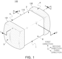
- a first direction may be defined as a direction in which first and second internal electrodes are alternately disposed while having a dielectric layer interposed therebetween, or a thickness (T) direction
- a second direction may be defined as a length (L) direction
- a third direction may be defined as a width (W) direction.
- the second direction and the third direction may be perpendicular to the first direction.
- FIG. 1 is a perspective view schematically showing a multilayer electronic component according to exemplary embodiment of the present disclosure.
- FIG. 2 is a cross-sectional view taken along line I-I' of FIG. 1 .
- FIG. 3 is a cross-sectional view taken along line II-II' of FIG. 1 .
- FIG. 6 is an enlarged view of a region A of FIG. 2
- FIG. 7 is an enlarged view of a region B of FIG. 3 .
- the body 110 may include the dielectric layer and the first and second internal electrodes 121 and 122 alternately disposed in the first direction while having the dielectric layer interposed therebetween.
- the plurality of dielectric layers included in the body 110 may be in a sintered state, and adjacent dielectric layers may be integrated with each other so that boundaries therebetween are not readily apparent without using a scanning electron microscope (SEM).
- SEM scanning electron microscope
- the body 110 may include the capacitance formation portion Ac, the first margin portion LM1 or LM2, and a second margin portion WM1 or WM2.
- the second margin portion WM1 or WM2 may basically prevent the internal electrode from being damaged due to the physical or chemical stress.
- the average thickness of the cover portion 112 or 113 may indicate its size in the first direction, and may have a value obtained by averaging the sizes of the cover portion 112 or 113 in the first direction, measured at five equally spaced points on upper or lower surface of the capacitance formation portion Ac.
- the external electrode 131 or 132 may include an electrode layer disposed on the body 110 and a plating layer formed on the electrode layer.
- the electrode layer may have the fired electrode and the resin-based electrode, sequentially formed on the body.
- the electrode layer may be formed by transferring a sheet including the conductive metal to the body or by transferring the sheet including the conductive metal to the fired electrode.
- a multilayer electronic component 100 may include: a body 110 having first and second surfaces 1 and 2 opposing each other in the first direction, third and fourth surfaces 3 and 4 connected to the first and second surfaces and opposing each other in the second direction, and fifth and sixth surfaces 5 and 6 connected to the first to fourth surfaces 1 to 4 and opposing each other in the third direction, and including a dielectric layer and first and second internal electrodes 121 and 122 alternately disposed in the first direction while having the dielectric layer interposed therebetween; a first external electrode 131 disposed on the third surface 3 and connected to the first internal electrode 121; and a second external electrode 132 disposed on the fourth surface 4 and connected to the second internal electrode 122.
- a first margin portion LM1 or LM2 is a region of the body that is disposed on one side surface or the other side surface of the capacitance formation portion Ac in the second direction and including an end 121b or 122b of the first or second internal electrode 121 or 122
- a second margin portion WM1 or WM2 is a region of the body that is disposed on one surface or the other surface of the capacitance formation portion Ac in the third direction
- a first region 111a is a region of the dielectric layer that is included in the capacitance formation portion Ac
- a second region 111b is a region of the dielectric layer that is included in the first margin portion LM1 or LM2
- a third region 111c is a region of the dielectric layer that is included in the second margin portion WM1 or WM2, at least one element of silicon (Si), aluminum (A
- the center where the first region 111a is disposed may indicate the region from 1/5 point (R1) to 4/5 point (R4) when the region of the dielectric layer that is included in the capacitance formation portion Ac is divided into five parts in the second direction or the third direction, and the region from point 1/3 (Q1) to point 2/3 (Q2) when the region of the dielectric layer that is included in the capacitance formation portion Ac divided into third parts in the first direction. That is, the first region 111a may indicate a region spaced apart from the first margin portion LM1 or LM2, the second margin portion WM1 or WM2, and the internal electrode 121 or 122 at regular intervals.
- FIG. 7 shows the dielectric layer disposed at the center of the capacitance formation portion Ac in the first direction. However, the description of the center where the first region 111a is disposed may be similarly applied to any dielectric layer.
- a content of at least one of silicon (Si), aluminum (Al), lithium (Li), copper (Cu), sodium (Na), and bismuth (Bi), included in the second region 111b may be 2 moles or more and 7 moles or less relative to 100 moles of titanium (Ti).
- At least one of manganese (Mn), chromium (Cr), vanadium (V), iron (Fe), nickel (Ni), cobalt (Co), tin (Sn), indium (In), gallium (Ga), zinc (Zn), lead (Pb), silver (Ag), palladium (Pd), platinum (Pt), Iridium (Ir), ruthenium (Ru), osmium (Os), yttrium (Y), erbium (Er), ytterbium (Yb), terbium (Tb), holmium (Ho), and dysprosium (Dy) may be the element included in at least one of the second region 111b and the third region 111c, and not substantially included in the first region 111a.
- the multilayer electronic component 100 may secure the same effect when manganese (Mn) is the element included in at least one of the second region 111b and the third region 111c and not substantially included in the first region 111a.
- the multilayer electronic component 100 may also secure the same effect when at least one of chromium (Cr), vanadium (V), iron (Fe), nickel (Ni), cobalt (Co), tin (Sn), indium (In), gallium (Ga), zinc (Zn), lead (Pb), silver (Ag), palladium (Pd), platinum (Pt), Iridium (Ir), ruthenium (Ru), osmium (Os), yttrium (Y), erbium (Er), ytterbium (Yb), terbium (Tb), holmium (Ho), and dysprosium (Dy) is the element included in at least one of the second region 111b and the third region 111c and not substantially included in the first region 111a
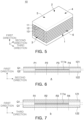
- FIG. 4 is an exploded perspective view schematically showing a method of manufacturing a body according to still another exemplary embodiment of the present disclosure.
- FIG. 5 is a perspective view schematically showing a ceramic multilayer body according to an exemplary embodiment of the present disclosure.
- internal electrode patterns 12 may be formed on a dielectric ceramic green sheet 11, and a process of stacking and compressing the plurality of sheets may be performed to form a ceramic multilayer body 10 in a state before sintering the body 110.
- the internal electrode patterns 12 may alternately expose one end and the other end in the second direction along the first direction without entirely covering the dielectric ceramic green sheet 11.
- the internal electrode pattern 12 may be fired to become first and second internal electrodes 121 and 122, and the dielectric ceramic green sheet 11 may be sintered to become a dielectric layer.
- the dielectric ceramic green sheet 11 may include a raw material forming the dielectric layer.
- the dielectric layer may use a material such as a barium titanate-based material, a lead composite perovskite-based material, a strontium titanate-based material, or the like.
- the barium titanate-based material may include barium titanate (BaTiO 3 )-based ceramic powders, and the ceramic powders may be, for example, BaTiO 3 or (Ba 1-x Ca x )TiO 3 (0 ⁇ x ⁇ 1), Ba(Ti 1-y Ca y )O 3 (0 ⁇ y ⁇ 1), (Ba 1-x Ca x )(Ti 1-y Zr y )O 3 (0 ⁇ x ⁇ 1, 0 ⁇ y ⁇ 1) or Ba(Ti 1-y Zr y )O 3 (0 ⁇ y ⁇ 1), in which calcium (Ca), zirconium (Zr) or the like is partially dissolved in BaTiO 3 .
- various ceramic additives, organic solvents, binders, dispersants and the like may be added to the ceramic powders based on a purpose of the present disclosure.
- a compensation pattern 13 may be disposed on a region of the dielectric ceramic green sheet 11 where the internal electrode pattern 12 is not disposed.
- the compensation pattern 13 may include at least one element not included in the dielectric ceramic green sheet 11.
- the element included in the compensation pattern 13 and not included in the dielectric ceramic green sheet 11 may be at least one of magnesium (Mg), silicon (Si), aluminum (Al), lithium (Li), copper (Cu), sodium (Na), bismuth (Bi), manganese (Mn), chromium (Cr), vanadium (V), iron (Fe), nickel (Ni), cobalt (Co), tin (Sn), indium (In), gallium (Ga), zinc (Zn), lead (Pb), silver (Ag), palladium (Pd), platinum (Pt), Iridium (Ir), ruthenium (Ru), osmium (Os), yttrium (Y), erbium (Er), ytterbium (Yb), terbium (Tb),
- the compensation pattern 13 may cover an entire portion of the dielectric ceramic green sheet 11 on which the internal electrode pattern 12 is not disposed.
- the compensation pattern 13 may cover the entire portion of the dielectric ceramic green sheet 11 on which the internal electrode pattern 12 is not disposed when the internal electrode pattern 12 is spaced apart from one end of the dielectric ceramic green sheet 11 in the second direction and both ends of the dielectric ceramic green sheet 11 in the third direction.
- the element in the compensation pattern 13 may be diffused into the dielectric ceramic green sheet 11 through a sintering process to form first to third regions 111a, 111b, and 111c of the dielectric layer.
- the element included in the compensation pattern 13 and not included in the dielectric ceramic green sheet 11 may not be diffused into the first region 111a of the dielectric layer that is included in a capacitance formation portion Ac during the sintering process, which may be adjusted by changing the distribution and sintering condition of the element included in the compensation pattern 13 and not included in the dielectric ceramic green sheet 11.
- the ceramic multilayer body 10 may include the internal electrode pattern 12 and the dielectric ceramic green sheet 11 which are alternately disposed in the first direction to have first and second surfaces 1 and 2 opposing each other in the first direction, third and fourth surfaces 3 and 4 connected to the first and second surfaces 1 and 2 and opposing each other in the second direction, and fifth and sixth surfaces 5 and 6 connected to the first to fourth surfaces 1 to 4 and opposing each other in the third direction.
- the first to sixth surfaces in FIG. 5 may be sintered to become the first to sixth surfaces 1 to 6 of the body 110.
- the content of the element included in the first region 111a or the second region 111b may be obtained by polishing the multilayer electronic component 100 to its center in the third direction to expose the cross sections in the first and second directions, then dividing the cross section in the first direction and the second direction into three parts, i.e., upper, lower, and middle parts, in the first direction, and then measuring an average value of the contents of the element at three or more 5 um x 5 um regions equally spaced from each other in each of the upper, lower, and middle parts in the second direction by using the transmission electron microscope-energy dispersive x-ray spectroscopy (TEM-EDX).
- TEM-EDX transmission electron microscope-energy dispersive x-ray spectroscopy
- Mean time to failure is obtained by performing the measurement for 80 samples at 105°C and 8 Vr conditions, in which an average value of the mean time to failures (MTTF) is taken by measuring a time until the value of the insulation resistance (IR) falls to 10000 ⁇ or less.
- Table 1 shows the result of evaluating the BDV characteristic of the multilayer electronic component by adjusting the content of magnesium (Mg) (relative to 100 moles of titanium (Ti)) included in the second region 111b when magnesium (Mg) is the element included in the second region 111b and not included in the first region 111a.
- Test no. Content of Mg in second region BDV (V) 1 0 mol 72.05 2 1 mol 81.53 3 2 mol 83.89 4 3 mol 84.44 5 4 mol 84.63 6 5 mol 83.21 7 6 mol 69.83
- the BDV characteristic of the multilayer electronic component is improved when the content of magnesium (Mg) included in the second region 111b is 1 mole or more (relative to 100 moles of titanium (Ti)) when magnesium (Mg) is the element included in the second region 111b and not included in the first region 111a.
- the BDV characteristic of the multilayer electronic component 100 is deteriorated when the content of magnesium (Mg) in the second region 111b is more than 5 moles (relative to 100 moles of titanium (Ti)).
- Table 2 shows the result of evaluating the BDV characteristic of the multilayer electronic component by adjusting the content of silicon (Si) (relative to 100 moles of titanium (Ti)) included in the second region 111b when silicon (Si) is the element included in the second region 111b and not included in the first region 111a.
- Test No. Content of Si in second region BDV (V) 1 0 mol 72.05 2 1 mol 72.16 3 2 mol 83.61 4 3 mol 87.13 5 4 mol 84.75 6 5 mol 89.13 7 6 mol 87.91 8 7 mol 83.16 9 8 mol 65.39
- the BDV characteristic of the multilayer electronic component is improved when the content of silicon (Si) included in the second region 111b is 2 mole or more (relative to 100 moles of titanium (Ti)) when silicon (Si) is the element included in the second region 111b and not included in the first region 111a.
- the BDV characteristic of the multilayer electronic component 100 is deteriorated when the content of silicon (Si) in the second region 111b is more than 7 moles (relative to 100 moles of titanium (Ti)).
- the high-temperature reliability of the multilayer electronic component is significantly improved when the content of manganese (Mn) included in the second region 111b is 1 mole or more (relative to 100 moles of titanium (Ti)) when magnesium (Mg) is the element included in the second region 111b and not included in the first region 111a.
- the high-temperature reliability of the multilayer electronic component 100 is significantly deteriorated when the content of manganese (Mn) in the second region 111b is more than 3 moles (relative to 100 moles of titanium (Ti)).
Landscapes
- Engineering & Computer Science (AREA)
- Power Engineering (AREA)
- Manufacturing & Machinery (AREA)
- Microelectronics & Electronic Packaging (AREA)
- Chemical & Material Sciences (AREA)
- Ceramic Engineering (AREA)
- Inorganic Chemistry (AREA)
- Fixed Capacitors And Capacitor Manufacturing Machines (AREA)
- Ceramic Capacitors (AREA)
Applications Claiming Priority (1)
| Application Number | Priority Date | Filing Date | Title |
|---|---|---|---|
| KR1020220188435A KR20240105939A (ko) | 2022-12-29 | 2022-12-29 | 적층형 전자 부품 |
Publications (2)
| Publication Number | Publication Date |
|---|---|
| EP4394828A2 true EP4394828A2 (fr) | 2024-07-03 |
| EP4394828A3 EP4394828A3 (fr) | 2024-12-04 |
Family
ID=89321826
Family Applications (1)
| Application Number | Title | Priority Date | Filing Date |
|---|---|---|---|
| EP23220004.8A Pending EP4394828A3 (fr) | 2022-12-29 | 2023-12-22 | Composant électronique multicouche |
Country Status (5)
| Country | Link |
|---|---|
| US (1) | US20240222020A1 (fr) |
| EP (1) | EP4394828A3 (fr) |
| JP (1) | JP2024096025A (fr) |
| KR (1) | KR20240105939A (fr) |
| CN (1) | CN118280731A (fr) |
Families Citing this family (1)
| Publication number | Priority date | Publication date | Assignee | Title |
|---|---|---|---|---|
| WO2026034335A1 (fr) * | 2024-08-07 | 2026-02-12 | 株式会社村田製作所 | Condensateur céramique multicouche |
Family Cites Families (4)
| Publication number | Priority date | Publication date | Assignee | Title |
|---|---|---|---|---|
| JP6955363B2 (ja) * | 2017-04-17 | 2021-10-27 | 太陽誘電株式会社 | 積層セラミックコンデンサおよびその製造方法 |
| KR101987214B1 (ko) * | 2017-10-13 | 2019-06-10 | 삼성전기주식회사 | 적층 세라믹 커패시터 |
| JP6596547B2 (ja) * | 2018-07-10 | 2019-10-23 | 太陽誘電株式会社 | 積層セラミックコンデンサ |
| KR102041755B1 (ko) * | 2019-05-24 | 2019-11-06 | 삼성전기주식회사 | 적층 세라믹 커패시터 |
-
2022
- 2022-12-29 KR KR1020220188435A patent/KR20240105939A/ko active Pending
-
2023
- 2023-12-13 US US18/538,670 patent/US20240222020A1/en active Pending
- 2023-12-21 JP JP2023215862A patent/JP2024096025A/ja active Pending
- 2023-12-22 EP EP23220004.8A patent/EP4394828A3/fr active Pending
- 2023-12-28 CN CN202311837650.7A patent/CN118280731A/zh active Pending
Also Published As
| Publication number | Publication date |
|---|---|
| EP4394828A3 (fr) | 2024-12-04 |
| US20240222020A1 (en) | 2024-07-04 |
| CN118280731A (zh) | 2024-07-02 |
| JP2024096025A (ja) | 2024-07-11 |
| KR20240105939A (ko) | 2024-07-08 |
Similar Documents
| Publication | Publication Date | Title |
|---|---|---|
| KR102584977B1 (ko) | 세라믹 전자 부품 및 그 제조 방법 | |
| US8773840B2 (en) | Monolithic ceramic electronic component | |
| US11476047B2 (en) | Multilayer electronic component | |
| US11699554B2 (en) | Multi-layered ceramic electronic component | |
| KR20220088099A (ko) | 세라믹 전자 부품 | |
| KR20220101911A (ko) | 적층형 전자 부품 | |
| US20230411076A1 (en) | Ceramic electronic component | |
| KR20220081633A (ko) | 적층형 전자 부품 및 유전체 조성물 | |
| CN112908696B (zh) | 多层电子组件 | |
| EP4394828A2 (fr) | Composant électronique multicouche | |
| EP4379762B1 (fr) | Composant électronique multicouche (mlcc) interface améliorée avec les électrodes externes | |
| KR20220092246A (ko) | 적층형 전자 부품 | |
| KR20220104513A (ko) | 적층형 전자 부품 | |
| US20230197349A1 (en) | Multilayer electronic component | |
| CN118352161A (zh) | 多层电子组件 | |
| KR102776256B1 (ko) | 적층형 전자 부품 | |
| US12573556B2 (en) | Multilayer electronic component | |
| US12387876B2 (en) | Multilayer electronic component | |
| US20250210262A1 (en) | Multilayer electronic component | |
| US12555720B2 (en) | Multilayer electronic component with enhanced electrode connectivity using Ni and Al oxide | |
| US12322556B2 (en) | Multilayer electronic component | |
| US20260120950A1 (en) | Multilayer electronic component | |
| EP4425513A1 (fr) | Répartition molaire de ba ti et si dans les couches dielectriques pour des composants céramiques multicouches | |
| KR20220083295A (ko) | 적층형 전자 부품 |
Legal Events
| Date | Code | Title | Description |
|---|---|---|---|
| PUAI | Public reference made under article 153(3) epc to a published international application that has entered the european phase |
Free format text: ORIGINAL CODE: 0009012 |
|
| STAA | Information on the status of an ep patent application or granted ep patent |
Free format text: STATUS: THE APPLICATION HAS BEEN PUBLISHED |
|
| AK | Designated contracting states |
Kind code of ref document: A2 Designated state(s): AL AT BE BG CH CY CZ DE DK EE ES FI FR GB GR HR HU IE IS IT LI LT LU LV MC ME MK MT NL NO PL PT RO RS SE SI SK SM TR |
|
| REG | Reference to a national code |
Ref country code: DE Ref legal event code: R079 Free format text: PREVIOUS MAIN CLASS: H01G0004120000 Ipc: H01G0004300000 |
|
| RIC1 | Information provided on ipc code assigned before grant |
Ipc: H01G 4/232 20060101ALN20240808BHEP Ipc: C04B 35/465 20060101ALN20240808BHEP Ipc: B32B 18/00 20060101ALI20240808BHEP Ipc: C04B 35/462 20060101ALI20240808BHEP Ipc: H01G 4/228 20060101ALI20240808BHEP Ipc: H01G 4/12 20060101ALI20240808BHEP Ipc: H01G 4/30 20060101AFI20240808BHEP |
|
| PUAL | Search report despatched |
Free format text: ORIGINAL CODE: 0009013 |
|
| AK | Designated contracting states |
Kind code of ref document: A3 Designated state(s): AL AT BE BG CH CY CZ DE DK EE ES FI FR GB GR HR HU IE IS IT LI LT LU LV MC ME MK MT NL NO PL PT RO RS SE SI SK SM TR |
|
| RIC1 | Information provided on ipc code assigned before grant |
Ipc: H01G 4/232 20060101ALN20241029BHEP Ipc: C04B 35/465 20060101ALN20241029BHEP Ipc: B32B 18/00 20060101ALI20241029BHEP Ipc: C04B 35/462 20060101ALI20241029BHEP Ipc: H01G 4/228 20060101ALI20241029BHEP Ipc: H01G 4/12 20060101ALI20241029BHEP Ipc: H01G 4/30 20060101AFI20241029BHEP |
|
| STAA | Information on the status of an ep patent application or granted ep patent |
Free format text: STATUS: REQUEST FOR EXAMINATION WAS MADE |
|
| 17P | Request for examination filed |
Effective date: 20250527 |