EP4394835A1 - Procédé de commande d'économie d'énergie pour contacteur - Google Patents
Procédé de commande d'économie d'énergie pour contacteur Download PDFInfo
- Publication number
- EP4394835A1 EP4394835A1 EP22877801.5A EP22877801A EP4394835A1 EP 4394835 A1 EP4394835 A1 EP 4394835A1 EP 22877801 A EP22877801 A EP 22877801A EP 4394835 A1 EP4394835 A1 EP 4394835A1
- Authority
- EP
- European Patent Office
- Prior art keywords
- contactor
- coil
- full
- energy
- diode
- Prior art date
- Legal status (The legal status is an assumption and is not a legal conclusion. Google has not performed a legal analysis and makes no representation as to the accuracy of the status listed.)
- Pending
Links
Images

Classifications
-
- H—ELECTRICITY
- H01—ELECTRIC ELEMENTS
- H01H—ELECTRIC SWITCHES; RELAYS; SELECTORS; EMERGENCY PROTECTIVE DEVICES
- H01H47/00—Circuit arrangements not adapted to a particular application of the relay and designed to obtain desired operating characteristics or to provide energising current
- H01H47/02—Circuit arrangements not adapted to a particular application of the relay and designed to obtain desired operating characteristics or to provide energising current for modifying the operation of the relay
- H01H47/04—Circuit arrangements not adapted to a particular application of the relay and designed to obtain desired operating characteristics or to provide energising current for modifying the operation of the relay for holding armature in attracted position, e.g. when initial energising circuit is interrupted; for maintaining armature in attracted position, e.g. with reduced energising current
-
- H—ELECTRICITY
- H01—ELECTRIC ELEMENTS
- H01H—ELECTRIC SWITCHES; RELAYS; SELECTORS; EMERGENCY PROTECTIVE DEVICES
- H01H47/00—Circuit arrangements not adapted to a particular application of the relay and designed to obtain desired operating characteristics or to provide energising current
- H01H47/22—Circuit arrangements not adapted to a particular application of the relay and designed to obtain desired operating characteristics or to provide energising current for supplying energising current for relay coil
- H01H47/32—Energising current supplied by semiconductor device
-
- H—ELECTRICITY
- H01—ELECTRIC ELEMENTS
- H01H—ELECTRIC SWITCHES; RELAYS; SELECTORS; EMERGENCY PROTECTIVE DEVICES
- H01H47/00—Circuit arrangements not adapted to a particular application of the relay and designed to obtain desired operating characteristics or to provide energising current
- H01H47/02—Circuit arrangements not adapted to a particular application of the relay and designed to obtain desired operating characteristics or to provide energising current for modifying the operation of the relay
- H01H47/04—Circuit arrangements not adapted to a particular application of the relay and designed to obtain desired operating characteristics or to provide energising current for modifying the operation of the relay for holding armature in attracted position, e.g. when initial energising circuit is interrupted; for maintaining armature in attracted position, e.g. with reduced energising current
- H01H47/043—Circuit arrangements not adapted to a particular application of the relay and designed to obtain desired operating characteristics or to provide energising current for modifying the operation of the relay for holding armature in attracted position, e.g. when initial energising circuit is interrupted; for maintaining armature in attracted position, e.g. with reduced energising current making use of an energy accumulator
-
- H—ELECTRICITY
- H01—ELECTRIC ELEMENTS
- H01H—ELECTRIC SWITCHES; RELAYS; SELECTORS; EMERGENCY PROTECTIVE DEVICES
- H01H47/00—Circuit arrangements not adapted to a particular application of the relay and designed to obtain desired operating characteristics or to provide energising current
- H01H47/22—Circuit arrangements not adapted to a particular application of the relay and designed to obtain desired operating characteristics or to provide energising current for supplying energising current for relay coil
- H01H47/226—Circuit arrangements not adapted to a particular application of the relay and designed to obtain desired operating characteristics or to provide energising current for supplying energising current for relay coil for bistable relays
-
- H—ELECTRICITY
- H01—ELECTRIC ELEMENTS
- H01H—ELECTRIC SWITCHES; RELAYS; SELECTORS; EMERGENCY PROTECTIVE DEVICES
- H01H51/00—Electromagnetic relays
- H01H51/01—Relays in which the armature is maintained in one position by a permanent magnet and freed by energisation of a coil producing an opposing magnetic field
-
- H—ELECTRICITY
- H01—ELECTRIC ELEMENTS
- H01H—ELECTRIC SWITCHES; RELAYS; SELECTORS; EMERGENCY PROTECTIVE DEVICES
- H01H51/00—Electromagnetic relays
- H01H51/22—Polarised relays
- H01H51/2209—Polarised relays with rectilinearly movable armature
-
- H—ELECTRICITY
- H01—ELECTRIC ELEMENTS
- H01H—ELECTRIC SWITCHES; RELAYS; SELECTORS; EMERGENCY PROTECTIVE DEVICES
- H01H47/00—Circuit arrangements not adapted to a particular application of the relay and designed to obtain desired operating characteristics or to provide energising current
- H01H47/02—Circuit arrangements not adapted to a particular application of the relay and designed to obtain desired operating characteristics or to provide energising current for modifying the operation of the relay
- H01H47/18—Circuit arrangements not adapted to a particular application of the relay and designed to obtain desired operating characteristics or to provide energising current for modifying the operation of the relay for introducing delay in the operation of the relay
Definitions
- the energy-saving control method further includes an energy-saving control circuit.
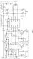
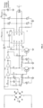
- the energy-saving control circuit includes a full-bridge driver chip U1 for controlling the function of the contactor KM, the energy storage circuit connected to the control power supply, a voltage-stabilizing circuit connected to the energy storage circuit and configured to send an input voltage to the full-bridge driver chip U1 after voltage stabilization, a voltage signal detection and regulation circuit, a three-stage inverter connected to the voltage signal detection and regulation circuit, a pull-in delay regulation circuit for generating a pull-in voltage and a contactor KM connecting delay, and a release delay regulation circuit for controlling a release voltage and a contactor KM disconnecting delay.
- the pull-in delay regulation circuit and the release delay regulation circuit are both connected to the three-stage inverter.
- An input terminal of the inverter U2B is connected to an output terminal of the inverter U2A, and an input terminal of the inverter U2A is connected to a positive electrode of the control power supply through a resistor R4 and a resistor R5, and both terminals of the resistor R5 are connected in parallel with a capacitor C3 and a Zener diode DW1.
- the energy storage circuit includes an energy storage capacitor C1 for storing electric energy, the energy storage capacitor C1 is connected to the control power supply through a buffer resistor R8, and the control power supply is used to charge the energy storage capacitor C1.
- Step of disconnecting the contactor is as follows: when the control power supply is turned off, the energy storage circuit discharges to provide released electric energy to the coil 4 of the contactor KM.
- the released electric energy outputs a pulse with opposite polarity to a pull-in voltage of the coil 4 of the contactor KM via a full-bridge drive control circuit, the full-bridge driver U1, after the full-bridge driver chip U1 receives a power-off signal of a voltage signal detection and regulation circuit, an input voltage of the energy storage circuit is sent into the coil 4 after polarity switching.
- the full-bridge driver chip U1 outputs a reverse pulse voltage signal, and the coil 4 of the contactor KM generates a magnetic force in a direction opposite to that of an existing magnetic force to disconnect the main loop contact 1 of the contactor KM.
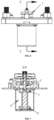
- the direction of the magnetic force of the magnetic field is reversed, and the action mechanism 2 of the contactor KM acts towards a direction opposite to the direction when pulling in, making the main loop contact 1 of the contactor KM disconnected.
- the main circuit contact 1 of the contactor KM is kept in a disconnected state under the action of a release permanent magnet 3.
- the energy-saving control method further includes an energy-saving control circuit.
- the energy-saving control circuit includes a full-bridge driver chip U1 for controlling the function of the contactor KM, the energy storage circuit connected to the control power supply, a voltage-stabilizing circuit connected to the energy storage circuit and configured to send an input voltage to the full-bridge driver chip U1 after voltage stabilization, a voltage signal detection and regulation circuit connected to the control power supply and configured for the detection and regulation and filtering overvoltage protection of an input voltage signal, a three-stage inverter connected to the voltage signal detection and regulation circuit, a pull-in delay regulation circuit for generating a pull-in voltage and a contactor KM connecting delay, and a release delay regulation circuit 6 for controlling a release voltage and a contactor KM disconnecting delay.
- the pull-in delay regulation circuit and the release delay regulation circuit 6 are both connected to the three-stage inverter.
- the three-stage inverter includes an inverter U2A, an inverter U2B, and an inverter U2C connected in series.
- the energy storage capacitor C1 is charged by the energy storage circuit, and meanwhile, the coil 4 of the contactor KM generates an attractive magnetic force after receiving a pulse voltage signal, making the action mechanism 2 of the contactor KM connected under the combined action of the attractive magnetic force generated by the coil 4 of the contactor KM and the attractive magnetic force of the pull-in permanent magnet 5, and a signal is sent to the full-bridge driver chip U1 through the pull-in delay regulation circuit.
- the full-bridge driver chip U1 after receiving the signal, controls to turn off a voltage of the coil 4 of the contactor KM, the coil 4 of the contactor KM loses power, and the main loop contact 1 of the contactor KM is kept in a connected state under the action of the pull-in permanent magnet 5.
- step of disconnecting the contactor when the control power supply is turned off, after the full-bridge driver chip U1 receives a power-off signal of the voltage signal detection and regulation circuit, an electric energy voltage of the energy storage capacitor C1 in the energy storage circuit is sent into the coil 4 of the contactor KM after polarity switching, the coil (4) of the contactor KM generates a magnetic force in an opposite direction of an existing magnetic force, i.e., a reverse magnetic force, which makes the contact KM break away from the attractive magnetic force of the pull-in permanent magnet 5 to be disconnected.
- the action mechanism 2 of the contactor KM is attached to the release permanent magnet 3, the main loop contact 1 of the contactor KM is disconnected, and then a signal is sent by the release delay regulation circuit 6 to the full-bridge driver chip U1 to make the coil 4 of the contactor KM lose power, and the main loop contact 1 of the contactor KM is kept in a disconnected state under the action of the release permanent magnet 3.
- the positive electrode of the control power supply is further connected to a diode D1, the diode D1 is further connected to a VBB pin of the full-bridge driver chip U1 to provide a working voltage for the coil 4 of the contactor KM.
- the diode D1 When the control power supply is turned off, the diode D1 is reversely cut off, and the output terminal of the inverter U2C outputs a high electrical level signal to the full-bridge driver chip U1, and the full-bridge driving chip U1 outputs a voltage after polarity switching.
- the control power supply is powered on, a positive electrode voltage provides a power supply voltage for the VBB pin of the full-bridge driver chip U1 via the diode D1, i.e., the working voltage of the coil 4 of the contactor KM, and meanwhile, the energy storage capacitor C1 is charged through the buffer resistor R8.
- a voltage with a regulated voltage of 5V formed through voltage division by the resistor R1 and the Zener diode DW2 is connected to an analog voltage input Vref pin of U1.
- the positive electrode of the control power supply is connected to an input terminal of the inverter U2A of the three-stage inverter formed by the inverter U2A, the inverter U2B, and the inverter U2C connected in series after being connected to the resistor R4 and the resistor R5 for voltage division.
- the output terminal of the inverter U2B acquires an electrical level signal synchronous with the input, and the output terminal of the U2C acquires an electrical level signal having a phase opposite to that of the input terminal of the inverter U2A, is connected to the IN1 pin of the full-bridge driver chip U1, and is connected to the IN2 pin of the full-bridge driver chip U1 through the resistor R6.
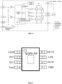
- a truth table of the full-bridge driver chip U1 is shown in Table 1.
- Table 1 Truth table IN1 IN2 OUT1 OUT2 Function 0 1 L H Pull-in 1 0 H L Release 0 0 Z Z Hold
- the OUT1 pin of the full-bridge driver chip U1 outputs a power supply voltage with positive polarity
- the OUT2 pin of the full-bridge driving chip U1 outputs a power supply voltage with negative polarity.
- the coil 4 of the contactor KM is energized and is kept closed under the action of the permanent magnet.
- the output terminal of the inverter U2B is connected to the base electrode of the triode V1 after being connected to the resistor R2 and the resistor R3 in series for voltage division, so as to charge the capacitor C2.
- the threshold depends on the charging time of the C2, the electrical level of the IN2 pin of the full-bridge driver chip U1 is pulled down, and according to the truth table of the full-bridge driver chip U1, the OUT1 pin and the OUT2 pin of the full-bridge drive pin U1 output high resistance, the coil 4 of the contactor KM loses power, and the current of the coil 4 is zero.
- the contactor is kept in a pull-in state all the time by a permanent magnet, and the current of the coil 4 of the contactor KM is zero, in this case, the coil of the contactor KM has zero power consumption.
- the total energy consumption of a voltage-division resistor, a voltage-stabilizing tube and a chip in the line in this state is about 0.2 W, while the holding power of the general contactor is about 10 W-30 W, and compared with the power consumption of 0.2 W, it may be considered that the coil 4 of the contactor KM is in a micro-power consumption state.
- the release characteristics, i.e., release voltage values, of the power supply voltage in the slow drop process can be regulated by adjusting a resistance ratio of the resistor R2 and the resistor R3.
- the pull-in characteristics, i.e., pull-in voltage values, of the power supply voltage in the slow rising process can be regulated by adjusting a resistance ratio of the resistor R4 and the resistor R5.
- the Zener diode DW1 is used for preventing the inverter from being damaged when the power supply voltage rises or is debugged.
- the diodes D2, D3, D4 and D5 can absorb back electromotive force generated when the coil of the contactor KM works, and the resistor R7 is a current-limiting protection sampling resistor.
- a transformer is arranged at an input terminal of the AC-DC conversion circuit.
Landscapes
- Physics & Mathematics (AREA)
- Electromagnetism (AREA)
- Engineering & Computer Science (AREA)
- Power Engineering (AREA)
- Relay Circuits (AREA)
Applications Claiming Priority (2)
| Application Number | Priority Date | Filing Date | Title |
|---|---|---|---|
| CN202111168468.8A CN113611572B (zh) | 2021-10-08 | 2021-10-08 | 一种接触器的节能控制方法 |
| PCT/CN2022/110370 WO2023056777A1 (fr) | 2021-10-08 | 2022-08-04 | Procédé de commande d'économie d'énergie pour contacteur |
Publications (2)
| Publication Number | Publication Date |
|---|---|
| EP4394835A1 true EP4394835A1 (fr) | 2024-07-03 |
| EP4394835A4 EP4394835A4 (fr) | 2025-09-17 |
Family
ID=78310746
Family Applications (1)
| Application Number | Title | Priority Date | Filing Date |
|---|---|---|---|
| EP22877801.5A Pending EP4394835A4 (fr) | 2021-10-08 | 2022-08-04 | Procédé de commande d'économie d'énergie pour contacteur |
Country Status (3)
| Country | Link |
|---|---|
| EP (1) | EP4394835A4 (fr) |
| CN (1) | CN113611572B (fr) |
| WO (1) | WO2023056777A1 (fr) |
Families Citing this family (2)
| Publication number | Priority date | Publication date | Assignee | Title |
|---|---|---|---|---|
| CN113611572B (zh) * | 2021-10-08 | 2022-02-01 | 南京全宁电器有限公司 | 一种接触器的节能控制方法 |
| CN114415580B (zh) * | 2022-03-31 | 2022-06-14 | 南京全宁电器有限公司 | 一种无弧分断交流电路的控制方法 |
Family Cites Families (15)
| Publication number | Priority date | Publication date | Assignee | Title |
|---|---|---|---|---|
| GB1447494A (en) * | 1973-03-22 | 1976-08-25 | Gen Electric Co Ltd | Electric circuit arrangements for energising electromagnetic relays |
| JPS61128437A (ja) * | 1984-11-26 | 1986-06-16 | 松下電工株式会社 | 電磁接触器 |
| DE19641188C1 (de) * | 1996-09-24 | 1998-01-08 | Siemens Ag | Schaltungsanordnung zur Energieversorgung eines Schaltgerät-Magnetantriebs |
| CN2483827Y (zh) * | 2001-02-11 | 2002-03-27 | 林李杰 | 自保持节能型停电自动释放式交流接触器 |
| CN101587799B (zh) * | 2008-05-22 | 2013-02-13 | 旭丽电子(广州)有限公司 | 继电器驱动模块及应用该继电器驱动模块的电子装置 |
| CN101441956B (zh) * | 2008-10-31 | 2011-03-23 | 上海电科电器科技有限公司 | 一种低压开关电器电磁铁控制电路 |
| DE102011080226B4 (de) * | 2011-08-01 | 2024-01-25 | Bayerische Motoren Werke Aktiengesellschaft | Fahrzeug mit einem Stromverteiler und einem Steuergerät |
| CN102709118B (zh) * | 2012-06-14 | 2014-05-07 | 浙江大学 | 一种交流接触器的节能器 |
| CN102842461A (zh) * | 2012-08-13 | 2012-12-26 | 华通机电股份有限公司 | 储能式节能交流接触器 |
| EP3185272A1 (fr) * | 2015-12-22 | 2017-06-28 | ABB Schweiz AG | Dispositif d'installation d'un système de commande d'un relais bistable |
| CN112435892A (zh) * | 2019-08-10 | 2021-03-02 | 胡春生 | 一种磁保持操作机构智能控制器 |
| CN210200635U (zh) * | 2019-08-10 | 2020-03-27 | 胡春生 | 一种磁保持操作机构智能控制器 |
| CN112397343B (zh) * | 2020-10-28 | 2023-10-20 | 温州大学 | 一种交流接触器及其抗晃电的智能电子控制装置 |
| CN113611572B (zh) * | 2021-10-08 | 2022-02-01 | 南京全宁电器有限公司 | 一种接触器的节能控制方法 |
| CN113871250B (zh) * | 2021-10-08 | 2025-05-13 | 南京全宁电器有限公司 | 一种高效节能的接触器控制电路 |
-
2021
- 2021-10-08 CN CN202111168468.8A patent/CN113611572B/zh active Active
-
2022
- 2022-08-04 WO PCT/CN2022/110370 patent/WO2023056777A1/fr not_active Ceased
- 2022-08-04 EP EP22877801.5A patent/EP4394835A4/fr active Pending
Also Published As
| Publication number | Publication date |
|---|---|
| EP4394835A4 (fr) | 2025-09-17 |
| WO2023056777A1 (fr) | 2023-04-13 |
| CN113611572B (zh) | 2022-02-01 |
| CN113611572A (zh) | 2021-11-05 |
Similar Documents
| Publication | Publication Date | Title |
|---|---|---|
| CN201440636U (zh) | 开关电源中功率开关管最大导通占空比的限制电路 | |
| CN112886640A (zh) | 限流电路和储能系统 | |
| CN117067945A (zh) | 一种电动车辆的动力电池的升压充电系统和方法 | |
| CN114415580B (zh) | 一种无弧分断交流电路的控制方法 | |
| CN113871250B (zh) | 一种高效节能的接触器控制电路 | |
| CN203377777U (zh) | 一种辅助电源的软起电路 | |
| CN103248349B (zh) | 电子式交流接触器 | |
| CN113611572B (zh) | 一种接触器的节能控制方法 | |
| CN109412466B (zh) | 汽轮机危急直流润滑油泵复合型启停装置及控制方法 | |
| CN202906730U (zh) | 一种用于led反激驱动电源的自关断启动控制电路 | |
| CN216353973U (zh) | 一种高效节能的接触器控制电路 | |
| CN203261305U (zh) | 新型电子式交流接触器 | |
| CN214506569U (zh) | 限流电路和储能系统 | |
| CN115732249B (zh) | 一种高压真空开关驱动电路 | |
| CN201693155U (zh) | 压铸机可编程控制器电磁阀控制板 | |
| CN101804454B (zh) | 压铸机可编程控制器电磁阀控制板 | |
| CN213402445U (zh) | 检测保护电路、装置及电器设备 | |
| CN214480541U (zh) | 一种电分电合及断电自动合闸的双稳态接触器 | |
| CN210359727U (zh) | 一种用于提高逆变式弧焊电源igbt工作可靠性的电路 | |
| CN202067728U (zh) | 断电吸持型永磁式接触器 | |
| CN209389778U (zh) | 一种旁路式双路供电切换系统 | |
| CN223390448U (zh) | 一种电压自适应交流接触器低压直流驱动电路 | |
| CN221304535U (zh) | 一种继电器倍压驱动电路及三相储能逆变器 | |
| CN205356777U (zh) | 一种照明节能旁路装置 | |
| CN217788280U (zh) | 一种继电器节能驱动电路 |
Legal Events
| Date | Code | Title | Description |
|---|---|---|---|
| STAA | Information on the status of an ep patent application or granted ep patent |
Free format text: STATUS: THE INTERNATIONAL PUBLICATION HAS BEEN MADE |
|
| PUAI | Public reference made under article 153(3) epc to a published international application that has entered the european phase |
Free format text: ORIGINAL CODE: 0009012 |
|
| STAA | Information on the status of an ep patent application or granted ep patent |
Free format text: STATUS: REQUEST FOR EXAMINATION WAS MADE |
|
| 17P | Request for examination filed |
Effective date: 20240329 |
|
| AK | Designated contracting states |
Kind code of ref document: A1 Designated state(s): AL AT BE BG CH CY CZ DE DK EE ES FI FR GB GR HR HU IE IS IT LI LT LU LV MC MK MT NL NO PL PT RO RS SE SI SK SM TR |
|
| DAV | Request for validation of the european patent (deleted) | ||
| DAX | Request for extension of the european patent (deleted) | ||
| REG | Reference to a national code |
Ref country code: DE Ref legal event code: R079 Free format text: PREVIOUS MAIN CLASS: H01H0047040000 Ipc: H01H0047220000 |
|
| A4 | Supplementary search report drawn up and despatched |
Effective date: 20250819 |
|
| RIC1 | Information provided on ipc code assigned before grant |
Ipc: H01H 47/22 20060101AFI20250812BHEP Ipc: H01H 51/22 20060101ALI20250812BHEP Ipc: H01H 47/32 20060101ALI20250812BHEP Ipc: H01H 47/18 20060101ALI20250812BHEP |