EP4394901A1 - Diode électroluminescente et dispositif électroluminescent doté de celle-ci - Google Patents
Diode électroluminescente et dispositif électroluminescent doté de celle-ci Download PDFInfo
- Publication number
- EP4394901A1 EP4394901A1 EP22861683.5A EP22861683A EP4394901A1 EP 4394901 A1 EP4394901 A1 EP 4394901A1 EP 22861683 A EP22861683 A EP 22861683A EP 4394901 A1 EP4394901 A1 EP 4394901A1
- Authority
- EP
- European Patent Office
- Prior art keywords
- layer
- light emitting
- active layer
- emitting diode
- light
- Prior art date
- Legal status (The legal status is an assumption and is not a legal conclusion. Google has not performed a legal analysis and makes no representation as to the accuracy of the status listed.)
- Pending
Links
Images







Classifications
-
- H—ELECTRICITY
- H10—SEMICONDUCTOR DEVICES; ELECTRIC SOLID-STATE DEVICES NOT OTHERWISE PROVIDED FOR
- H10H—INORGANIC LIGHT-EMITTING SEMICONDUCTOR DEVICES HAVING POTENTIAL BARRIERS
- H10H20/00—Individual inorganic light-emitting semiconductor devices having potential barriers, e.g. light-emitting diodes [LED]
- H10H20/80—Constructional details
- H10H20/81—Bodies
- H10H20/822—Materials of the light-emitting regions
- H10H20/824—Materials of the light-emitting regions comprising only Group III-V materials, e.g. GaP
- H10H20/825—Materials of the light-emitting regions comprising only Group III-V materials, e.g. GaP containing nitrogen, e.g. GaN
-
- H—ELECTRICITY
- H10—SEMICONDUCTOR DEVICES; ELECTRIC SOLID-STATE DEVICES NOT OTHERWISE PROVIDED FOR
- H10H—INORGANIC LIGHT-EMITTING SEMICONDUCTOR DEVICES HAVING POTENTIAL BARRIERS
- H10H20/00—Individual inorganic light-emitting semiconductor devices having potential barriers, e.g. light-emitting diodes [LED]
- H10H20/80—Constructional details
- H10H20/81—Bodies
- H10H20/811—Bodies having quantum effect structures or superlattices, e.g. tunnel junctions
- H10H20/812—Bodies having quantum effect structures or superlattices, e.g. tunnel junctions within the light-emitting regions, e.g. having quantum confinement structures
-
- H—ELECTRICITY
- H10—SEMICONDUCTOR DEVICES; ELECTRIC SOLID-STATE DEVICES NOT OTHERWISE PROVIDED FOR
- H10H—INORGANIC LIGHT-EMITTING SEMICONDUCTOR DEVICES HAVING POTENTIAL BARRIERS
- H10H20/00—Individual inorganic light-emitting semiconductor devices having potential barriers, e.g. light-emitting diodes [LED]
- H10H20/80—Constructional details
- H10H20/81—Bodies
- H10H20/813—Bodies having a plurality of light-emitting regions, e.g. multi-junction LEDs or light-emitting devices having photoluminescent regions within the bodies
-
- H—ELECTRICITY
- H10—SEMICONDUCTOR DEVICES; ELECTRIC SOLID-STATE DEVICES NOT OTHERWISE PROVIDED FOR
- H10H—INORGANIC LIGHT-EMITTING SEMICONDUCTOR DEVICES HAVING POTENTIAL BARRIERS
- H10H20/00—Individual inorganic light-emitting semiconductor devices having potential barriers, e.g. light-emitting diodes [LED]
- H10H20/80—Constructional details
- H10H20/81—Bodies
- H10H20/814—Bodies having reflecting means, e.g. semiconductor Bragg reflectors
-
- H—ELECTRICITY
- H10—SEMICONDUCTOR DEVICES; ELECTRIC SOLID-STATE DEVICES NOT OTHERWISE PROVIDED FOR
- H10H—INORGANIC LIGHT-EMITTING SEMICONDUCTOR DEVICES HAVING POTENTIAL BARRIERS
- H10H20/00—Individual inorganic light-emitting semiconductor devices having potential barriers, e.g. light-emitting diodes [LED]
- H10H20/80—Constructional details
- H10H20/81—Bodies
- H10H20/819—Bodies characterised by their shape, e.g. curved or truncated substrates
- H10H20/821—Bodies characterised by their shape, e.g. curved or truncated substrates of the light-emitting regions, e.g. non-planar junctions
-
- H—ELECTRICITY
- H10—SEMICONDUCTOR DEVICES; ELECTRIC SOLID-STATE DEVICES NOT OTHERWISE PROVIDED FOR
- H10H—INORGANIC LIGHT-EMITTING SEMICONDUCTOR DEVICES HAVING POTENTIAL BARRIERS
- H10H20/00—Individual inorganic light-emitting semiconductor devices having potential barriers, e.g. light-emitting diodes [LED]
- H10H20/80—Constructional details
- H10H20/81—Bodies
- H10H20/8215—Bodies characterised by crystalline imperfections, e.g. dislocations; characterised by the distribution of dopants, e.g. delta-doping
-
- H—ELECTRICITY
- H10—SEMICONDUCTOR DEVICES; ELECTRIC SOLID-STATE DEVICES NOT OTHERWISE PROVIDED FOR
- H10H—INORGANIC LIGHT-EMITTING SEMICONDUCTOR DEVICES HAVING POTENTIAL BARRIERS
- H10H20/00—Individual inorganic light-emitting semiconductor devices having potential barriers, e.g. light-emitting diodes [LED]
- H10H20/80—Constructional details
- H10H20/85—Packages
- H10H20/857—Interconnections, e.g. lead-frames, bond wires or solder balls
-
- H—ELECTRICITY
- H10—SEMICONDUCTOR DEVICES; ELECTRIC SOLID-STATE DEVICES NOT OTHERWISE PROVIDED FOR
- H10H—INORGANIC LIGHT-EMITTING SEMICONDUCTOR DEVICES HAVING POTENTIAL BARRIERS
- H10H29/00—Integrated devices, or assemblies of multiple devices, comprising at least one light-emitting semiconductor element covered by group H10H20/00
- H10H29/10—Integrated devices comprising at least one light-emitting semiconductor component covered by group H10H20/00
- H10H29/14—Integrated devices comprising at least one light-emitting semiconductor component covered by group H10H20/00 comprising multiple light-emitting semiconductor components
- H10H29/142—Two-dimensional arrangements, e.g. asymmetric LED layout
Definitions
- Exemplary embodiments relate to a light emitting diode, and more particularly, to a light emitting diode emitting light having multi-bands at a single chip level.
- Exemplary embodiments provide a light emitting diode that emits light having a spectrum of multi-bands at a single chip level, and a light emitting device having the same.
- Exemplary embodiments provide a light emitting diode and a light emitting device to easily implement mixed-color light having a desired color coordinate.
- a light emitting diode includes: a first conductivity type nitride semiconductor layer; a V-pit generation layer disposed on the n-type nitride semiconductor layer and having a V-pit; a lower active layer disposed on the V-pit generation layer; an upper active layer disposed on the lower active layer; an intermediate layer disposed between the lower active layer and the upper active layer; and a second conductivity type nitride semiconductor layer disposed on the upper active layer, in which the lower active layer and the upper active layer emit light having different peak wavelengths from each other.
- the upper active layer includes a first well region disposed over the flat surface of the V-pit generation layer and a second well region formed along the inclined surface of the V-pit, a well layer of the first well region may include a more In content than that of a well layer of the second well region, and the second well region may not emit light.
- the light emitting diode may further include a lower step coverage layer disposed between the intermediate layer and the lower active layer, and the lower step coverage layer may include a nitride-based semiconductor layer including Al.
- the first conductivity type semiconductor layer 23 may include an n-type contact layer.
- a nucleation layer and a high-temperature buffer layer may be additionally formed.
- the nucleation layer, the high-temperature buffer layer, and the first conductivity type nitride semiconductor layer 23 may be continuously formed on the substrate 21 in the chamber, and threading dislocations formed in the high-temperature buffer layer may be transferred to the first conductivity type nitride semiconductor layer 23.
- the first conductivity type nitride semiconductor layer 23 may have a first refraction index n1, and a surface in which the first conductivity type nitride semiconductor layer 23 is in contact with a patterned substrate 21 may be an interface in which a refraction index thereof changes.
- the substrate 21 may have a refraction index smaller than that of the first conductivity type nitride semiconductor layer 23, and thus, when light generated in the active layers 30 and 60 is incident on the substrate 21, it may be refracted at an angle greater than an incident angle with respect to a normal of the interface. Accordingly, by employing the substrate 21 having the refraction index smaller than that of the first conductivity type nitride semiconductor layer 23, light may be evenly distributed from an upper surface to a side surface of the substrate 21.
- the V-pit generation layer 29 is disposed on the first conductivity type nitride semiconductor layer 23.
- the V-pit generation layer 29 may be formed of, for example, a GaN layer.
- the V-pit generation layer 29 may be grown at a temperature relatively lower than that for growing the first conductivity type nitride semiconductor layer 23, for example, about 900°C, and thus, the V-pits 29v are formed in the V-pit generation layer 29.
- the V-pit generation layer 29 may be formed to have a thickness smaller than that of the first conductivity type nitride semiconductor layer 23, and for example, to have a thickness of about 450 nm to 600 nm. Sizes of the V-pits 29v formed in the V-pit generation layer 29 may be adjusted through a growth condition and a growth time of the V-pit generation layer 29. In an exemplary embodiment, a maximum width of an inlet of the V-pit 29v formed in the V-pit generation layer 29 may generally exceed about 200 nm.
- the V-pit generation layer 29 is a single layer, the inventive concepts are not limited thereto, and may be multiple layers.
- the V-pit generation layer 29 may include at least two of GaN, AlGaN, InGaN, or AlGaInN layers.
- the thickness of the V-pit generation layer 29 particularly affects the size of the V-pit 29v. Moreover, the size of the V-pit 29v is considered to play a major role in generating light having a spectrum of multi-bands.
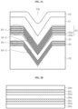
- the lower active layer 60, the intermediate layer 50, and the upper active layer 30 may be disposed on the V-pit generation layer 29.
- the lower active layer 60 and the upper active layer 30 may have a multi-quantum well structure, and may emit light by recombination of electrons and holes.
- a plurality of regions having the third refraction index n3 may be disposed, and a region having the fourth refraction index n4 may be disposed between the regions having the third refraction index n3.
- the intermediate layer 50 may have a seventh refraction index n7.
- the seventh refraction index n7 may be smaller than the third refraction index n3 and the fourth refraction index n4, and may be smaller than the fifth refraction index n5 and the sixth refraction index n6. Since the layer having a relatively small refraction index is disposed between the active layers 30 and 60, internal scattering of light is increased to increase a light extraction efficiency.
- an internal quantum efficiency of the nitride-based semiconductor layer emitting blue light is generally higher than that of the nitride-based semiconductor layer emitting yellow light. Accordingly, although the lower active layer 60 is disposed under the upper active layer 30, the intensity of light emitted from the lower active layer 60 may be made to be higher than that of light emitted from the upper active layer 30.
- the second conductivity type nitride semiconductor layer 33 is disposed on the upper active layer 30. As shown in FIG. 1 and FIG. 2A , a current blocking layer 31 may be disposed between the second conductivity type nitride semiconductor layer 33 and the upper active layer 30.
- the current blocking layer 31 may include, for example, a p-type AlxGa1-xN layer.
- the second conductivity type nitride semiconductor layer 33 may be formed of a semiconductor layer doped with a p-type impurity, for example, GaN.
- the second conductivity type nitride semiconductor layer 33 may be formed as a single layer or multiple layers, and may include a p-type contact layer.
- the second conductivity type nitride semiconductor layer 33 may have an eighth refraction index n9.
- the second conductivity type nitride semiconductor layer 33 may have a lower light absorption rate than those of the well regions 30-1, 30-2, 60-1, and 60-2 with respect to light generated in the light emitting diode 100. As shown in FIG. 1 , the second conductivity type nitride semiconductor layer 33 may have a concave groove over the V-pit 29v.
- the second conductivity type nitride semiconductor layer 33 does not completely fill the V-pit 29v, light loss that may occur while light generated in the second well region 30-2 in the V-pit 29v passes through the second conductivity type nitride semiconductor layer 33 may be reduced.
- FIG. 4 is a graph showing an electroluminescence (EL) spectrum of the light emitting diode fabricated according to the first exemplary embodiment of the present disclosure
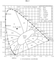
- FIG. 5 is a graph in which color coordinates of the light emitting diode showing the spectrum of FIG. 4 are marked on a CIE 1931 color space chromaticity diagram.
- EL electroluminescence
- the light emitting diode emits light having two peak wavelengths ( ⁇ 1, ⁇ 2), and there is a difference in intensities and full widths at half maximum (FWHM) In particular, an intensity of a shorter wavelength band is greater than that of a longer wavelength band. In addition, a full width at half maximum of the longer wavelength band is larger than that of the shorter wavelength band. According to this, it can be seen that an intensity of light emitted from a lower active layer 60 is higher than that of light emitted from an upper active layer 30. In addition, since the lower active layer 60 has a better crystal quality, a full width at half maximum of a spectrum of light emitted from the lower active layer 60 is narrower than that of a spectrum of light emitted from the upper active layer 30. Meanwhile, it can be seen that the shorter wavelength band and the longer wavelength band partially overlap.
- an interval between the two peak wavelengths ⁇ 1 and ⁇ 2 may be in a range of about 50 nm to 100 nm.
- the peak wavelength is not limited to two, and may have more peak wavelengths.
- FIG. 8 is a schematic cross-sectional view illustrating a light emitting diode 200 according to a second exemplary embodiment of the present disclosure
- FIG. 9 is a schematic partial cross-sectional view illustrating an enlarged portion of FIG. 8
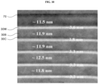
- FIG.10 is a transmission electron microscopy (TEM) photograph of the light emitting diode fabricated according to the second exemplary embodiment of the present disclosure, which shows a region corresponding to a partial region of FIG. 9 .
- TEM transmission electron microscopy
- the light emitting diode 200 includes a lower active layer 60, an intermediate layer 50, an upper active layer 30, and an upper step coverage layer 70.
- the light emitting diode 200 may also include a substrate 21, a first conductivity type nitride semiconductor layer 23, a V-pit generation layer 29, a current blocking layer 31, and a second conductivity type nitride semiconductor layer 33.
- the substrate 21, the first conductivity type nitride semiconductor layer 23, the V-pit generation layer 29, the lower active layer 60, the intermediate layer 50, the upper active layer 30, the current blocking layer 31, and the second conductivity type nitride semiconductor layer 33 are same as those described with reference to FIG. 1 , FIG. 2A, and FIG. 2B , detailed descriptions thereof will be omitted to avoid redundancy.
- the upper step coverage layer 70 prevents light from being generated in a second well region 30-2 of the upper active layer 30. That is, in the illustrated exemplary embodiment, light is not emitted from the second well region 30-2 by introducing the upper step coverage layer 70.
- the first well region 30-1 and the second well region 30-2 of the upper active layer may emit light of a specific peak wavelength depending on an In content in each well layer.
- an In composition of the second well region 30-2 depends on an In composition of the first well region 30-1, it is difficult to control the In content in the second well region 30-2. Accordingly, it is difficult to control the wavelength of light emitted from the second well region 30-2.
- light of a desired multi-bands may be easily implemented by preventing light from being emitted from the second well region 30-2, and allowing the lower active layer 60 to emit light of a shorter wavelength band.
- step coverage layer 70 by improving a crystal quality through reducing threading dislocations by using a V-pit 29v and also introducing the step coverage layer 70, it is possible to easily implement light of a spectrum of multi-bands having a desired peak wavelength.
- electrical characteristics such as turn on voltage may be improved.
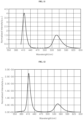
- FIG. 11 is a photoluminescence (PL) measurement graph of the light emitting diode fabricated according to the second exemplary embodiment of the present disclosure
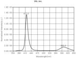
- FIG. 12 is an EL (electroluminescence) measurement graph of the light emitting diode fabricated according to the second exemplary embodiment of the present disclosure.
- light emitted from the upper active layer 30 and the lower active layer 60 have two peak wavelengths.
- the peak wavelength of light emitted from the lower active layer 60 is about 413 nm
- two peak wavelengths appear because light is not emitted from the second well region 30-2 of the upper active layer 30.
- an injection of holes into the second well region 30-2 may be blocked, and thus, it is judged that light is not generated in the second well region 30-2 of the upper active layer 30.
- a shorter wavelength band and a longer wavelength band do not overlap but are spaced apart from each other.
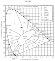
- FIG. 13 is a graph in which color coordinates of the light emitting diode fabricated according to the second exemplary embodiment are marked on the CIE 1931 color space chromaticity diagram.
- White light having a relatively low color temperature is emitted.
- White light may be implemented using light of multi-bands emitted within a single light emitting diode.
- Table 3 shows a correlation between complementary color wavelengths for implementing white, and white light may be implemented by designing the upper active layer 30 and the lower active layer 60 so as to emit light of a complementary color.
- Complementary Color Luminous Intensity Ratio ⁇ 1(nm) ⁇ 2(nm) P( ⁇ 2)/P( ⁇ 1) 380 ⁇ 400 540 ⁇ 570 0.000642 ⁇ 0.0785 400 ⁇ 420 540 ⁇ 570 0.0785 ⁇ 0.89 420 ⁇ 430 540 ⁇ 570 0.89 ⁇ 1.42 430 ⁇ 450 540 ⁇ 570 1.42 ⁇ 1.79 450 ⁇ 470 540 ⁇ 570 1.79 ⁇ 1.09 470 ⁇ 480 570 ⁇ 600 1.09 ⁇ 0.81 480 ⁇ 490 600 ⁇ 630 0.81 ⁇ 0.668
- ⁇ 1 is a peak wavelength of light emitted from the lower active layer 60
- ⁇ 2 is a peak wavelength of light emitted from the upper active layer 30.
- the relationship of the complementary color wavelengths targets white light in coordinates x: 0.205 ⁇ 0.495 and y: 0.19 ⁇ 0.45.
- the light emitting diode 200 has been exemplarily described as implementing white light, the inventive concepts are not limited thereto.
- Mixed light of various colors may be implemented using light emitted from the lower active layer 60 and the upper active layer 30.
- the upper step coverage layer 70 blocks light from being generated in the second well region 30-2 of the upper active layer 30, and thus, not only white light but also light of various colors may be implemented with the single light emitting diode by easily controlling the composition of the light emitting diode.
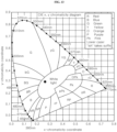
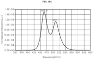
- FIG. 14A is an electroluminescence (EL) measurement graph of another light emitting diode fabricated according to the second exemplary embodiment of the present disclosure
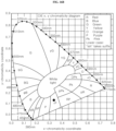
- FIG. 14B is a graph in which color coordinates of another light emitting diode fabricated according to the second exemplary embodiment are marked on the CIE 1931 color space chromaticity diagram.
- EL electroluminescence
- a first peak wavelength is about 465 nm by light emitted from the upper active layer 30 and the lower active layer 60
- light having a spectrum of multi-bands is emitted with a second peak wavelength of about 513.1 nm
- a cyan region of light having color coordinates corresponding to a inner region connecting a, b, c, and d of color coordinates a(0.012, 0.494), b(0.2, 0.4), c(0.2, 0.32), and d(0.04, 0.32) is implemented.
- An In content in the lower active layer 60 was about 16%
- an In content in the upper active layer 30 was about 22%.
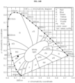
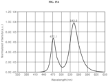
- FIG. 15A is an electroluminescence (EL) measurement graph of another light emitting diode fabricated according to the second exemplary embodiment of the present disclosure
- FIG. 15B is a graph in which color coordinates of another light emitting diode fabricated according to the second exemplary embodiment are marked on the CIE 1931 color space chromaticity diagram.
- EL electroluminescence
- a first peak wavelength is about 472.1 nm by light emitted from the upper active layer 30 and the lower active layer 60
- light having a spectrum of multi-bands is emitted with a second peak wavelength of about 543.6 nm
- a greenish blue region of light having a color coordinate x: 0.26, y: 0.50 is implemented.
- An In content in the lower active layer 60 was about 17%
- an In content in the upper active layer 30 was about 24%.
- FIG. 16A is an electroluminescence (EL) measurement graph of another light emitting diode fabricated according to the second exemplary embodiment of the present disclosure
- FIG. 16B is a graph in which color coordinates of another light emitting diode fabricated according to the second exemplary embodiment are marked on the CIE 1931 color space chromaticity diagram.
- EL electroluminescence
- a first peak wavelength is about 417 nm by light emitted from the upper active layer 30 and the lower active layer 60, and light having a spectrum of multi-bands is emitted with a second peak wavelength of about 602 nm, and a color coordinate x: 0.32, y: 0.17 represents a color of a purple region.
- an InGaN well layer was used to emit light having a peak wavelength of 600 nm or more in the first well region 30-1 of the upper active layer 30.
- An In content in the lower active layer 60 was about 9%, and an In content in the upper active layer 30 was about 31%.
- FIG. 17A is an electroluminescence (EL) measurement graph of another light emitting diode fabricated according to the second exemplary embodiment of the present disclosure
- FIG. 17B is a graph in which color coordinates of another light emitting diode fabricated according to the second exemplary embodiment are marked on the CIE 1931 color space chromaticity diagram.
- EL electroluminescence
- a first peak wavelength is about 452.7 nm by light emitted from the upper active layer 30 and the lower active layer 60, and light having a spectrum of multi-bands is emitted with a second peak wavelength about 582 nm, a color coordinate x: 0.50, y: 0.43 represents a color of a yellow orange region.
- An In content in the upper active layer 30 was about 29%.
- a desired white light or other mixed-color light may be implemented with a single light emitting diode by controlling the peak wavelength of light emitted from the lower active layer 60 and the upper active layer 30.
- cyan light located within a region surrounded by color coordinates of four points: (0.012, 0.494), (0.2, 0.4), (0.2, 0.32), (0.04, 0.32) may be implemented by the light emitting diode without using a phosphor.
- FIG. 18 is a schematic cross-sectional view illustrating a light emitting diode 300 according to a third exemplary embodiment of the present disclosure.
- the lower step coverage layer 80 is disposed on the lower active layer 60, and blocks injection of holes into a second well region 60-2 of a lower active layer 60 to prevent light from being generated in the second well region 60-2. Furthermore, the lower step coverage layer 80 relieves a stress of an upper active layer 30 to improve a radiation efficiency of the light emitting diode 300.
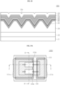
- FIG. 19A is a schematic plan view illustrating a light emitting device 1000 according to an exemplary embodiment of the present disclosure
- FIG. 19B is a schematic cross-sectional view taken along line A-A' of its corresponding view shown in FIG. 19A
- FIG. 19C is a schematic cross-sectional view taken along line B-B' of its corresponding view shown in FIG. 19A .
- the first lead 121a and the second lead 121b may be formed of a conductive material, for example, a metal. Bottom surfaces of the first lead 121a and the second lead 121b may be partially removed by half-cutting, and thus, may include relatively thin regions.
- the first lead 121a and the second lead 121b may include anchors 121e protruding upward from upper surfaces of the leads 121a and 121b as shown in FIG. 19C .
- the anchors 121e may be formed on edges of the leads 121a and 121b, and in particular, may be disposed over half-cut regions. The anchors 121e prevent the leads 121a and 121b from being separated from the housing 123.
- the light emitting diode chips 125a and 125b may be disposed on the first lead 121a, and may be electrically connected to the first and second leads 121a and 121b through the bonding wires 129.
- the light emitting diode chips 125a and 125b may include the light emitting diodes 100, 200, and 300 described in the previous embodiments.
- the light emitting diode chips 125a and 125b may emit light of a same color, without being limited thereto, and may emit light of different colors.
- the molding member 131 covers the light emitting diode chips 125a and 125b.
- the molding member 131 may fill the cavity of the housing 123.
- the molding member 131 may be formed of transparent silicone.
- the molding member 131 may not include a phosphor. Since the light emitting diode chips 125a and 125b emit mixed-color light, a desired mixed-color light may be implemented without using a phosphor 133.
- the molding member 131 may include the phosphor 133. Since the light emitting diode chips 125a and 125b emit mixed-color light, an amount of the phosphor 133 used may be relatively less than that of a conventional light emitting device.
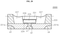
- the housing 223 covers portions of upper surfaces of the leads 221a and 221b and portions of lower surfaces of the leads 221a and 221b.
- the housing 223 may fill the region in which the bottom surface is partially removed by half-cutting, and may fill the through-holes formed in the leads 221a and 221b.
Landscapes
- Led Devices (AREA)
Applications Claiming Priority (4)
| Application Number | Priority Date | Filing Date | Title |
|---|---|---|---|
| US202163236400P | 2021-08-24 | 2021-08-24 | |
| US202163240121P | 2021-09-02 | 2021-09-02 | |
| US17/892,189 US20230076963A1 (en) | 2021-08-24 | 2022-08-22 | Light emitting diode and light emitting device having the same |
| PCT/KR2022/012568 WO2023027474A1 (fr) | 2021-08-24 | 2022-08-23 | Diode électroluminescente et dispositif électroluminescent doté de celle-ci |
Publications (2)
| Publication Number | Publication Date |
|---|---|
| EP4394901A1 true EP4394901A1 (fr) | 2024-07-03 |
| EP4394901A4 EP4394901A4 (fr) | 2025-11-12 |
Family
ID=85323349
Family Applications (1)
| Application Number | Title | Priority Date | Filing Date |
|---|---|---|---|
| EP22861683.5A Pending EP4394901A4 (fr) | 2021-08-24 | 2022-08-23 | Diode électroluminescente et dispositif électroluminescent doté de celle-ci |
Country Status (3)
| Country | Link |
|---|---|
| US (1) | US20230076963A1 (fr) |
| EP (1) | EP4394901A4 (fr) |
| WO (1) | WO2023027474A1 (fr) |
Families Citing this family (1)
| Publication number | Priority date | Publication date | Assignee | Title |
|---|---|---|---|---|
| CN116454186A (zh) * | 2023-06-15 | 2023-07-18 | 江西兆驰半导体有限公司 | 发光二极管外延片及其制备方法、发光二极管 |
Family Cites Families (11)
| Publication number | Priority date | Publication date | Assignee | Title |
|---|---|---|---|---|
| DE102006039369A1 (de) * | 2005-12-30 | 2007-07-05 | Osram Opto Semiconductors Gmbh | LED-Halbleiterkörper und Verwendung eines LED-Halbleiterkörpers |
| KR20150078641A (ko) * | 2013-12-31 | 2015-07-08 | 일진엘이디(주) | v-피트를 구비하는 질화물 반도체 발광소자 및 그 제조 방법 |
| KR102335105B1 (ko) * | 2014-11-14 | 2021-12-06 | 삼성전자 주식회사 | 발광 소자 및 그의 제조 방법 |
| JP2018516466A (ja) * | 2015-06-05 | 2018-06-21 | オステンド・テクノロジーズ・インコーポレーテッド | 多重活性層へのキャリア注入を選定した発光構造 |
| DE102015112042B4 (de) * | 2015-07-23 | 2021-07-01 | OSRAM Opto Semiconductors Gesellschaft mit beschränkter Haftung | Optoelektronische Leuchtvorrichtung |
| KR102569461B1 (ko) * | 2015-11-30 | 2023-09-04 | 쑤저우 레킨 세미컨덕터 컴퍼니 리미티드 | 발광소자 및 이를 포함하는 조명장치 |
| CN105870286A (zh) * | 2016-04-22 | 2016-08-17 | 南昌大学 | 带V坑多量子阱多波长的GaN基LED外延结构及其制备方法 |
| WO2018128419A1 (fr) * | 2017-01-04 | 2018-07-12 | 엘지이노텍 주식회사 | Dispositif à semiconducteur et boîtier de dispositif électroluminescent le comportant |
| KR102320022B1 (ko) * | 2017-03-09 | 2021-11-02 | 서울바이오시스 주식회사 | 반도체 발광 소자 |
| US11557695B2 (en) * | 2020-02-04 | 2023-01-17 | Seoul Viosys Co., Ltd. | Single chip multi band LED |
| US20220216188A1 (en) * | 2021-01-06 | 2022-07-07 | Seoul Viosys Co., Ltd. | Light emitting device and light emitting module having the same |
-
2022
- 2022-08-22 US US17/892,189 patent/US20230076963A1/en active Pending
- 2022-08-23 EP EP22861683.5A patent/EP4394901A4/fr active Pending
- 2022-08-23 WO PCT/KR2022/012568 patent/WO2023027474A1/fr not_active Ceased
Also Published As
| Publication number | Publication date |
|---|---|
| EP4394901A4 (fr) | 2025-11-12 |
| US20230076963A1 (en) | 2023-03-09 |
| WO2023027474A1 (fr) | 2023-03-02 |
Similar Documents
| Publication | Publication Date | Title |
|---|---|---|
| US10559718B2 (en) | Light-emitting device having plural recesses in layers | |
| KR101611412B1 (ko) | 발광 소자 | |
| WO2007001098A1 (fr) | Nanostructure comprenant un puits quantique à base de nitrure et diode électroluminescente l'utilisant | |
| EP2908352B1 (fr) | Dispositif émetteur de lumière | |
| US12125945B2 (en) | Single chip multi band LED | |
| EP4141971A1 (fr) | Diode électroluminescente multi-bande à puce unique et ses applications | |
| US20250160071A1 (en) | Led lighting apparatus having improved color rendering and led filament | |
| US20260047239A1 (en) | Single chip multi band light emitting diode, light emitting device and light emitting module having the same | |
| EP4303939A1 (fr) | Diode électroluminescente multi-bande à puce unique et son procédé de fabrication | |
| EP4340050A1 (fr) | Diode électroluminescente multibande | |
| US20230076963A1 (en) | Light emitting diode and light emitting device having the same | |
| US12615886B2 (en) | Light emitting diode having multiple active layers and light emitting device having the same | |
| EP4496011A1 (fr) | Diode électroluminescente et dispositif émetteur de lumière doté de celle-ci | |
| EP4459680A1 (fr) | Élément électroluminescent et module électroluminescent le comprenant | |
| EP4447134A1 (fr) | Diode électroluminescente et élément électroluminescent doté de celle-ci | |
| US12604561B2 (en) | Mixed color light emitting device | |
| EP4401157A1 (fr) | Diode électroluminescente pour la production de lumière blanche | |
| KR102163978B1 (ko) | 발광소자 및 이를 구비하는 조명 시스템 | |
| KR20120011198A (ko) | 발광 소자, 발광 소자 패키지 및 발광 소자의 제조방법 | |
| KR20110132162A (ko) | 반도체 발광 소자 | |
| KR100608919B1 (ko) | 발광 소자 및 이의 제조 방법 | |
| KR20170105286A (ko) | 발광소자 및 이를 갖는 조명장치 | |
| KR20160056039A (ko) | 발광소자 및 조명시스템 | |
| KR20120035577A (ko) | 발광 소자 |
Legal Events
| Date | Code | Title | Description |
|---|---|---|---|
| STAA | Information on the status of an ep patent application or granted ep patent |
Free format text: STATUS: THE INTERNATIONAL PUBLICATION HAS BEEN MADE |
|
| PUAI | Public reference made under article 153(3) epc to a published international application that has entered the european phase |
Free format text: ORIGINAL CODE: 0009012 |
|
| STAA | Information on the status of an ep patent application or granted ep patent |
Free format text: STATUS: REQUEST FOR EXAMINATION WAS MADE |
|
| 17P | Request for examination filed |
Effective date: 20240322 |
|
| AK | Designated contracting states |
Kind code of ref document: A1 Designated state(s): AL AT BE BG CH CY CZ DE DK EE ES FI FR GB GR HR HU IE IS IT LI LT LU LV MC MK MT NL NO PL PT RO RS SE SI SK SM TR |
|
| DAV | Request for validation of the european patent (deleted) | ||
| DAX | Request for extension of the european patent (deleted) | ||
| REG | Reference to a national code |
Ref country code: DE Ref legal event code: R079 Free format text: PREVIOUS MAIN CLASS: H01L0033080000 Ipc: H10H0020813000 |
|
| A4 | Supplementary search report drawn up and despatched |
Effective date: 20251015 |
|
| RIC1 | Information provided on ipc code assigned before grant |
Ipc: H10H 20/813 20250101AFI20251009BHEP Ipc: H10H 20/81 20250101ALI20251009BHEP Ipc: H10H 20/821 20250101ALI20251009BHEP Ipc: H10H 20/825 20250101ALI20251009BHEP |