EP4395523A1 - Stratifié piézoélectrique, procédé de production pour stratifié piézoélectrique, matériau cible de pulvérisation et procédé de production pour matériau cible de pulvérisation - Google Patents
Stratifié piézoélectrique, procédé de production pour stratifié piézoélectrique, matériau cible de pulvérisation et procédé de production pour matériau cible de pulvérisation Download PDFInfo
- Publication number
- EP4395523A1 EP4395523A1 EP22861011.9A EP22861011A EP4395523A1 EP 4395523 A1 EP4395523 A1 EP 4395523A1 EP 22861011 A EP22861011 A EP 22861011A EP 4395523 A1 EP4395523 A1 EP 4395523A1
- Authority
- EP
- European Patent Office
- Prior art keywords
- film
- target material
- main surface
- powder
- piezoelectric
- Prior art date
- Legal status (The legal status is an assumption and is not a legal conclusion. Google has not performed a legal analysis and makes no representation as to the accuracy of the status listed.)
- Pending
Links
Images




Classifications
-
- C—CHEMISTRY; METALLURGY
- C23—COATING METALLIC MATERIAL; COATING MATERIAL WITH METALLIC MATERIAL; CHEMICAL SURFACE TREATMENT; DIFFUSION TREATMENT OF METALLIC MATERIAL; COATING BY VACUUM EVAPORATION, BY SPUTTERING, BY ION IMPLANTATION OR BY CHEMICAL VAPOUR DEPOSITION, IN GENERAL; INHIBITING CORROSION OF METALLIC MATERIAL OR INCRUSTATION IN GENERAL
- C23C—COATING METALLIC MATERIAL; COATING MATERIAL WITH METALLIC MATERIAL; SURFACE TREATMENT OF METALLIC MATERIAL BY DIFFUSION INTO THE SURFACE, BY CHEMICAL CONVERSION OR SUBSTITUTION; COATING BY VACUUM EVAPORATION, BY SPUTTERING, BY ION IMPLANTATION OR BY CHEMICAL VAPOUR DEPOSITION, IN GENERAL
- C23C14/00—Coating by vacuum evaporation, by sputtering or by ion implantation of the coating forming material
- C23C14/06—Coating by vacuum evaporation, by sputtering or by ion implantation of the coating forming material characterised by the coating material
- C23C14/08—Oxides
-
- C—CHEMISTRY; METALLURGY
- C04—CEMENTS; CONCRETE; ARTIFICIAL STONE; CERAMICS; REFRACTORIES
- C04B—LIME, MAGNESIA; SLAG; CEMENTS; COMPOSITIONS THEREOF, e.g. MORTARS, CONCRETE OR LIKE BUILDING MATERIALS; ARTIFICIAL STONE; CERAMICS; REFRACTORIES; TREATMENT OF NATURAL STONE
- C04B35/00—Shaped ceramic products characterised by their composition; Ceramics compositions; Processing powders of inorganic compounds preparatory to the manufacturing of ceramic products
- C04B35/01—Shaped ceramic products characterised by their composition; Ceramics compositions; Processing powders of inorganic compounds preparatory to the manufacturing of ceramic products based on oxide ceramics
- C04B35/495—Shaped ceramic products characterised by their composition; Ceramics compositions; Processing powders of inorganic compounds preparatory to the manufacturing of ceramic products based on oxide ceramics based on vanadium, niobium, tantalum, molybdenum or tungsten oxides or solid solutions thereof with other oxides, e.g. vanadates, niobates, tantalates, molybdates or tungstates
-
- C—CHEMISTRY; METALLURGY
- C23—COATING METALLIC MATERIAL; COATING MATERIAL WITH METALLIC MATERIAL; CHEMICAL SURFACE TREATMENT; DIFFUSION TREATMENT OF METALLIC MATERIAL; COATING BY VACUUM EVAPORATION, BY SPUTTERING, BY ION IMPLANTATION OR BY CHEMICAL VAPOUR DEPOSITION, IN GENERAL; INHIBITING CORROSION OF METALLIC MATERIAL OR INCRUSTATION IN GENERAL
- C23C—COATING METALLIC MATERIAL; COATING MATERIAL WITH METALLIC MATERIAL; SURFACE TREATMENT OF METALLIC MATERIAL BY DIFFUSION INTO THE SURFACE, BY CHEMICAL CONVERSION OR SUBSTITUTION; COATING BY VACUUM EVAPORATION, BY SPUTTERING, BY ION IMPLANTATION OR BY CHEMICAL VAPOUR DEPOSITION, IN GENERAL
- C23C14/00—Coating by vacuum evaporation, by sputtering or by ion implantation of the coating forming material
- C23C14/06—Coating by vacuum evaporation, by sputtering or by ion implantation of the coating forming material characterised by the coating material
- C23C14/08—Oxides
- C23C14/088—Oxides of the type ABO3 with A representing alkali, alkaline earth metal or Pb and B representing a refractory or rare earth metal
-
- C—CHEMISTRY; METALLURGY
- C23—COATING METALLIC MATERIAL; COATING MATERIAL WITH METALLIC MATERIAL; CHEMICAL SURFACE TREATMENT; DIFFUSION TREATMENT OF METALLIC MATERIAL; COATING BY VACUUM EVAPORATION, BY SPUTTERING, BY ION IMPLANTATION OR BY CHEMICAL VAPOUR DEPOSITION, IN GENERAL; INHIBITING CORROSION OF METALLIC MATERIAL OR INCRUSTATION IN GENERAL
- C23C—COATING METALLIC MATERIAL; COATING MATERIAL WITH METALLIC MATERIAL; SURFACE TREATMENT OF METALLIC MATERIAL BY DIFFUSION INTO THE SURFACE, BY CHEMICAL CONVERSION OR SUBSTITUTION; COATING BY VACUUM EVAPORATION, BY SPUTTERING, BY ION IMPLANTATION OR BY CHEMICAL VAPOUR DEPOSITION, IN GENERAL
- C23C14/00—Coating by vacuum evaporation, by sputtering or by ion implantation of the coating forming material
- C23C14/22—Coating by vacuum evaporation, by sputtering or by ion implantation of the coating forming material characterised by the process of coating
- C23C14/34—Sputtering
-
- C—CHEMISTRY; METALLURGY
- C23—COATING METALLIC MATERIAL; COATING MATERIAL WITH METALLIC MATERIAL; CHEMICAL SURFACE TREATMENT; DIFFUSION TREATMENT OF METALLIC MATERIAL; COATING BY VACUUM EVAPORATION, BY SPUTTERING, BY ION IMPLANTATION OR BY CHEMICAL VAPOUR DEPOSITION, IN GENERAL; INHIBITING CORROSION OF METALLIC MATERIAL OR INCRUSTATION IN GENERAL
- C23C—COATING METALLIC MATERIAL; COATING MATERIAL WITH METALLIC MATERIAL; SURFACE TREATMENT OF METALLIC MATERIAL BY DIFFUSION INTO THE SURFACE, BY CHEMICAL CONVERSION OR SUBSTITUTION; COATING BY VACUUM EVAPORATION, BY SPUTTERING, BY ION IMPLANTATION OR BY CHEMICAL VAPOUR DEPOSITION, IN GENERAL
- C23C14/00—Coating by vacuum evaporation, by sputtering or by ion implantation of the coating forming material
- C23C14/22—Coating by vacuum evaporation, by sputtering or by ion implantation of the coating forming material characterised by the process of coating
- C23C14/34—Sputtering
- C23C14/3407—Cathode assembly for sputtering apparatus, e.g. Target
- C23C14/3414—Metallurgical or chemical aspects of target preparation, e.g. casting, powder metallurgy
-
- H—ELECTRICITY
- H10—SEMICONDUCTOR DEVICES; ELECTRIC SOLID-STATE DEVICES NOT OTHERWISE PROVIDED FOR
- H10N—ELECTRIC SOLID-STATE DEVICES NOT OTHERWISE PROVIDED FOR
- H10N30/00—Piezoelectric or electrostrictive devices
- H10N30/01—Manufacture or treatment
- H10N30/07—Forming of piezoelectric or electrostrictive parts or bodies on an electrical element or another base
- H10N30/074—Forming of piezoelectric or electrostrictive parts or bodies on an electrical element or another base by depositing piezoelectric or electrostrictive layers, e.g. aerosol or screen printing
- H10N30/076—Forming of piezoelectric or electrostrictive parts or bodies on an electrical element or another base by depositing piezoelectric or electrostrictive layers, e.g. aerosol or screen printing by vapour phase deposition
-
- H—ELECTRICITY
- H10—SEMICONDUCTOR DEVICES; ELECTRIC SOLID-STATE DEVICES NOT OTHERWISE PROVIDED FOR
- H10N—ELECTRIC SOLID-STATE DEVICES NOT OTHERWISE PROVIDED FOR
- H10N30/00—Piezoelectric or electrostrictive devices
- H10N30/01—Manufacture or treatment
- H10N30/09—Forming piezoelectric or electrostrictive materials
- H10N30/093—Forming inorganic materials
- H10N30/097—Forming inorganic materials by sintering
-
- H—ELECTRICITY
- H10—SEMICONDUCTOR DEVICES; ELECTRIC SOLID-STATE DEVICES NOT OTHERWISE PROVIDED FOR
- H10N—ELECTRIC SOLID-STATE DEVICES NOT OTHERWISE PROVIDED FOR
- H10N30/00—Piezoelectric or electrostrictive devices
- H10N30/704—Piezoelectric or electrostrictive devices based on piezoelectric or electrostrictive films or coatings
-
- H—ELECTRICITY
- H10—SEMICONDUCTOR DEVICES; ELECTRIC SOLID-STATE DEVICES NOT OTHERWISE PROVIDED FOR
- H10N—ELECTRIC SOLID-STATE DEVICES NOT OTHERWISE PROVIDED FOR
- H10N30/00—Piezoelectric or electrostrictive devices
- H10N30/80—Constructional details
- H10N30/85—Piezoelectric or electrostrictive active materials
- H10N30/853—Ceramic compositions
- H10N30/8542—Alkali metal based oxides, e.g. lithium, sodium or potassium niobates
-
- C—CHEMISTRY; METALLURGY
- C04—CEMENTS; CONCRETE; ARTIFICIAL STONE; CERAMICS; REFRACTORIES
- C04B—LIME, MAGNESIA; SLAG; CEMENTS; COMPOSITIONS THEREOF, e.g. MORTARS, CONCRETE OR LIKE BUILDING MATERIALS; ARTIFICIAL STONE; CERAMICS; REFRACTORIES; TREATMENT OF NATURAL STONE
- C04B2235/00—Aspects relating to ceramic starting mixtures or sintered ceramic products
- C04B2235/02—Composition of constituents of the starting material or of secondary phases of the final product
- C04B2235/30—Constituents and secondary phases not being of a fibrous nature
- C04B2235/32—Metal oxides, mixed metal oxides, or oxide-forming salts thereof, e.g. carbonates, nitrates, (oxy)hydroxides, chlorides
- C04B2235/3201—Alkali metal oxides or oxide-forming salts thereof
Definitions
- Patent Document 1 discloses that adjusting a composition of a target material enables an adjustment of a composition of the KNN film.
- the composition ((K + Na)/Nb) of the target material is adjusted so that the composition ((K + Na)/Nb) of the KNN film falls within a predetermined range, spots where the composition of the KNN film does not satisfy the predetermined range sometimes appear on a main surface of the KNN film, in a case where the KNN film is deposited on a substrate with a large diameter of 3 inches or more by the sputtering method using a target material for mass production, specifically, a target material having an area of a surface to be exposed to plasma (sputter surface) of 44.2 cm 2 or more.
- the jig is composed of a material such as graphite and is configured to enable formation of sintered ceramics having an area of a main surface of 44.2 cm 2 or more and a thickness of 3 mm or more.
- the inventors have found that "unevenness of filling of raw material powders when filling the raw material powders in the jig" and "unevenness of sintering temperature (firing temperature) in a direction along the main surface of the sintered ceramics (unevenness of sintering temperature)" in producing the target material are factors causing the occurrence of spots with a low Vickers hardness and weak bonding between particles.
- a stack 10 (hereinafter also referred to as a piezoelectric stack 10) having a piezoelectric film according to this embodiment includes a substrate 1, a bottom electrode film 2 provided on the substrate 1, a piezoelectric film (piezoelectric thin film) 3 provided on the bottom electrode film 2, and a top electrode film 4 provided on the piezoelectric film 3.
- This embodiment describes an example in which one stacked structure (a structure in which at least the bottom electrode film 2, the piezoelectric film 3, and the top electrode film 4 are stacked) is provided on the single substrate 1.
- the substrate 1 has a main surface with a diameter of 3 inches or more.
- the substrate 1 has a circular outline in planar view.
- the outline of the substrate 1 is not limited to a circular shape.
- the substrate 1 preferably has a main surface in which an inscribed circle has a diameter of 3 inches or more.
- a single-crystal silicon (Si) substrate 1a provided with a surface oxide film (SiO 2 -film) 1b such as a thermal oxide film or chemical vapor deposition (CVD) oxide film, that is, a Si-substrate provided with a surface oxide film, can be suitably used.
- a Si-substrate 1a with an insulating film 1d comprising an insulating material other than SiO 2 on its surface can also be used, as illustrated in FIG. 2 .
- a Si-substrate 1a with an exposed Si-(100) or Si-(111) or the like on its surface that is, a Si-substrate without the surface oxide film 1b or insulating film 1d, can also be used.
- the bottom electrode film 2 can be provided using platinum (Pt), for example.
- the bottom electrode film 2 is a polycrystalline film.
- a polycrystalline film deposited using Pt is also referred to as a Pt-film.
- the Pt-film preferably has its (111) parallel to the main surface of the substrate 1 (including a case where (111) is inclined at an angle within ⁇ 5° with respect to the main surface of the substrate 1), that is, the Pt-film is preferably oriented in (111) direction.
- the "Pt-film is oriented in (111) direction” means that no peaks other than a peak due to (111) is observed in an X-ray diffraction pattern obtained by X-ray diffraction (XRD) as measured on a surface of a KNN film 3.
- a main surface of the bottom electrode film 2 (the surface to be a base of the piezoelectric film 3) is preferably composed of Pt-(111).
- the bottom electrode film 2 can be deposited by a sputtering method, an evaporation method, or the like.
- the bottom electrode film 2 can also be provided using various metals, in place of Pt, such as gold (Au), ruthenium (Ru), or iridium (Ir); alloys comprising these metals as main components; metal oxides such as strontium ruthenium oxide (SrRuO 3 , abbreviated as SRO) or lanthanum nickel oxide (LaNiO 3 , abbreviated as LNO); or the like.
- the bottom electrode film 2 can be a monolayer film provided using the above-described various metals, metal oxides, or the like.
- the bottom electrode film 2 can also be a stack of a Pt-film and a film mainly comprising SRO provided on the Pt-film, a stack of a Pt-film and a film mainly comprising LNO provided on the Pt-film, or the like.
- an adhesion layer 6 may also be provided between them.
- the adhesion layer 6 is mainly comprised, for example, titanium (Ti), tantalum (Ta), titanium oxide (TiO 2 ), nickel (Ni), ruthenium oxide (RuO 2 ), iridium oxide (IrO 2 ), zinc oxide (ZnO), or the like.
- the piezoelectric film 3 is a film comprising an alkali niobium oxide containing, for example, potassium (K), sodium (Na), niobium (Nb), and oxygen (O). That is, the piezoelectric film 3 is a film mainly composed of an alkali niobium oxide containing K, Na, Nb, and O.
- the piezoelectric film 3 can be provided using an alkali niobium oxide represented by a composition formula (K 1-x Na x )NbO 3 , that is, using a potassium sodium niobium oxide (KNN).
- the piezoelectric film 3 is a polycrystalline film of KNN (hereinafter also referred to as a KNN film 3).
- a crystal structure of KNN is a perovskite structure. That is, the KNN film 3 has the perovskite structure.
- Half or more of crystals in a crystal group constituting the KNN film 3 preferably have a columnar structure.
- a crystal system of KNN is considered to be a tetragonal crystal system.
- the KNN film 3 can be deposited by a method such as the sputtering method.
- the crystals constituting the KNN film 3 are preferentially oriented in (001) direction with respect to the main surface of the substrate 1 (or the Si-substrate 1a in a case where the substrate 1 is, for example, the Si-substrate 1a with the surface oxide film 1b or insulating film 1d). That is, a main surface of the KNN film 3 (a surface to be a base of the top electrode film 4) is preferably mainly composed of KNN-(001). For example, by depositing the KNN film 3 directly on the Pt-film (bottom electrode film 2) whose main surface is mainly composed of Pt-(111), the KNN film 3 whose main surface is mainly composed of KNN-(001) can be obtained.
- the "crystals constituting the KNN film 3 are oriented in (001) direction” means that (001) of crystals constituting the KNN film 3 are parallel or substantially parallel to the main surface of the substrate 1.
- the “crystals constituting the KNN film 3 are preferentially oriented in (001) direction” means that there are many crystals in which (001) is parallel or substantially parallel to the main surface of the substrate 1.
- 80 % or more of the crystals in the crystal group constituting the KNN film 3 are preferably oriented in (001) direction with respect to the main surface of the substrate 1. That is, an orientation ratio of the crystals constituting the KNN film 3 in (001) direction is, for example, preferably 80 % or more, and more preferably 90 % or more.
- (001) peak intensity in the above (Equation 1) refers to the intensity of a diffraction peak due to crystals oriented in (001) direction (i.e., crystals whose (001) is parallel to the main surface of the substrate 1) among the crystals constituting the KNN film 3, in the X-ray diffraction pattern obtained by performing XRD measurement on the KNN film 3.
- the (001) peak intensity is the intensity of a peak appearing within a range that 20 is 20° to 23°. When multiple peaks appear within the range that 20 is 20° to 23°, it refers to the intensity of the highest peak.
- the composition of K and Na in the KNN film 3 can be measured by atomic absorption spectrometry (AAS) or the like, and the composition of Nb can be measured by inductively coupled plasma atomic emission spectroscopy (ICP-AES) or the like.
- AAS atomic absorption spectrometry
- ICP-AES inductively coupled plasma atomic emission spectroscopy
- each sample obtained by cutting the KNN film 3 is decomposed by heating with sulfuric acid, nitric acid, hydrofluoric acid, and hydrochloric acid, and then dissolved by heating with dilute hydrogen peroxide water and dilute hydrofluoric acid to make up a constant volume.
- the resulting solution is subjected to AAS and ICP-AES to determine contents of K, Na, and Nb in the sample, which are then converted to an atomic number ratio thereof.
- the composition of K, Na, and Nb in the KNN film 3 can be determined.
- AAS can be performed using, for example, Z-2300, manufactured by Hitachi High-Technologies Corporation
- ICP-AES can be performed using, for example, PS3520VDDII, manufactured by Hitachi High-Tech Science Corporation.
- EDS energy-dispersive X-ray spectroscopy
- XRF X-ray fluorescence
- ICP-AES alone.
- it is difficult to accurately measure the above composition in the KNN film 3 due to low analytical sensitivity of K and Na so that the composition of the KNN film 3 cannot be evaluated accurately.
- the composition of the KNN film 3 can be evaluated accurately by measuring the composition of K, Na, and Nb of the KNN film 3 using both AAS and ICP-AES.
- the piezoelectric device module 30 can function as an actuator by connecting the voltage applicator 11a between the bottom electrode film 2 and the top electrode film 4 of the piezoelectric element 20.
- the KNN film 3 can be deformed by applying a voltage between the bottom electrode film 2 and the top electrode film 4 using the voltage applicator 11a. This deformation action allows various components connected to the piezoelectric device module 30 to be operated.
- applications of the piezoelectric device module 30 include, for example, a head for an inkjet printer, a MEMS mirror for a scanner, and a transducer for an ultrasonic generator.
- the top electrode film 4 is deposited on the KNN film 3 by the sputtering method, for example. Conditions for depositing the top electrode film 4 can be set similar to those for depositing the bottom electrode film 2 described above. Thus, the piezoelectric stack 10 such as that illustrated in FIG. 1 is obtained.
- a photoresist pattern as an etching mask for dry etching is provided on the piezoelectric stack 10 (e.g., top electrode film 4) by a photolithography process or the like.
- a precious metal film (metal mask) such as a Cr-film, Ni-film, Pt-film, or Ti-film may be provided as the etching mask by the sputtering method.
- dry etching is performed on the piezoelectric stack 10 (top electrode film 4, KNN film 3, and the like) using a gas containing a halogen element as an etching gas.
- the halogen element include chlorine (Cl), fluorine (F), or the like.
- BCh-gas, SiCl 4 -gas, Cl 2 -gas, CF 4 -gas, C 4 F 8 -gas, or the like can be used as the gas containing the halogen element.
- the target material 100 is composed of sintered ceramics including an oxide(s) containing K, Na, Nb, and O, that is, KNN-sintered ceramics. Crystal grains mainly constituting the KNN-sintered ceramics have a perovskite structure. In addition to the oxide containing K, Na, Nb, and O, the KNN-sintered ceramics may also sometimes contain a carbonate or an oxalate originating from raw materials described later.
- a composition of K, Na, and Nb ((K + Na)/Nb) in the target material 100 satisfies a relationship of 0.95 ⁇ (K + Na)/Nb ⁇ 1.2, preferably 1 ⁇ (K + Na)/Nb ⁇ 1.1.
- K, Na, and Nb in the formula of (K + Na)/Nb here represent the numbers of K-atoms, Na-atoms, and Nb-atoms contained per unit volume of the KNN-sintered ceramics, respectively.
- the composition of the target material 100 needs to be slightly richer in K and Na than the composition of the KNN film 3 to be deposited.
- the target material 100 may further contain, as a dopant, at least one element selected from the group consisting of Li, Mg, Ca, Sr, Ba, Bi, Sb, V, In, Ta, Mo, W, Cr, Ti, Zr, Hf, Sc, Y, La, Ce, Pr, Nd, Sm, Eu, Gd, Tb, Dy, Ho, Er, Tm, Yb, Lu, Cu, Zn, Ag, Mn, Fe, Co, Ni, Al, Si, Ge, Sn, and Ga.
- a concentration of such an element in the target material 100 can be, for example, 5 at% or less (when more than one of the above elements are contained, a total concentration thereof can be 5 at% or less).
- the target material 100 has a circular outline. That is, the target material 100 has the sputter surface 101 having a circular shape in planar view.
- the outline of the target material 100 may be various shapes other than the circular shape, such as an oval shape, a rectangular shape, or a polygonal shape.
- An area of the sputter surface 101 is 44.2 cm 2 or more.
- the sputter surface 101 has an area larger than the substrate 1 with a diameter of 3 inches.
- the "area of the sputter surface 101" as used herein means an area of the sputter surface 101 when viewed from the vertical upper side of the sputter surface 101.
- the target material 100 has a thickness of 3 mm or more.
- the upper limit of the thickness of the target material 100 is not particularly limited, but can be 20 mm or less, for example.
- the "the Vickers hardness of the sputter surface 101 is 150 or more over the entire inner region of the sputter surface 101, excluding its periphery” means that, as illustrated in FIG. 6 , when the hardness is measured at measurement points set at 1 cm intervals in a grid pattern over a region 101b of the sputter surface 101, excluding a region (periphery) 101a having a width of 5 mm from an edge of the sputter surface 101 (i.e., a region located inside a region having a width of 5mm from the edge), the Vickers hardness is 150 or more at all measurement points (37 points in a case where the sputter surface 101 has a circular outline with its area of 44.2 cm 2 ).
- FIG. 6 illustrates the measurement points of the Vickers hardness, indicated by marks • (black circles).
- the "entire inner region of the sputter surface 101, excluding its periphery” in this specification is also described as "the entire sputter surface region”.
- the Vickers hardness is 150 or more over the entire sputter surface region
- the occurrence of cracks on the sputter surface 101 can be suppressed during pre-sputtering or sputter deposition.
- the occurrence of abnormal electrical discharge can be avoided over the entire sputter surface region during sputter deposition. Therefore, regions with locally increased temperature can be avoided from appearing on the sputter surface 101 during sputter deposition, and local volatilization of K and Na from the sputter surface 101 can also be avoided.
- the KNN film 3 with a large diameter in which the composition of K, Na, and Nb satisfies the relationship of 0.94 ⁇ (K + Na)/Nb ⁇ 1.03 over the entire main surface region, can be obtained.
- the inventors have already confirmed that when the Vickers hardness is 150 or more over the entire sputter surface region, even the target material 100 with a large diameter having the area of the sputter surface 101 of 44.2 cm 2 or more and the thickness of 3 mm or more does not occur any spots with weak bonding between particles over the entire sputter surface region.
- the powder comprising the compound of K, the powder comprising the compound of Na, and the powder comprising the compound of Nb are prepared.
- the "powder comprising a compound of K" as used herein means powder containing the compound of K as a main component, and it may include a case in which the powder consists of the compound of K, as well as a case in which the powder contains powders of other compounds in addition to the powder, which is the main component, of the compound of K.
- the respective powders are mixed (wet mixed) using a mixer such as a ball mill or a bead mill.
- a mixer such as a ball mill or a bead mill.
- Conditions for mixing are exemplified as follows.
- the jig 208 is configured such that it can be put into a processing chamber 201 included in a hot press apparatus 200 described later and such that it is not damaged due to a pressure applied by a pressure applicator 217.
- the "area of the main surface” as used herein means an area of the main surface of the sintered ceramics when viewed from the vertical upper side.
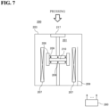
- the hot press process (hot press sintering) is performed using, for example, the hot press apparatus 200 illustrated in FIG. 7 . That is, while applying a predetermined pressure to a mixture 210 filled in the jig 208 and compressing it, the mixture 210 in the jig 208 is heated at a predetermined temperature, to obtain sintered ceramics.
- the hot press apparatus 200 illustrated in FIG. 7 includes a processing container 203 comprising SUS or the like and including the processing chamber 201 therein.
- the pressure applicator 217 e.g., a hydraulic press type pressure applicator 217) is provided inside the processing chamber 201.
- the pressure applicator 217 is configured to be able to apply a predetermined pressure to the mixture 210 filled in the jig 208.
- a heater 207 that heats the mixture 210 in the jig 208 to a predetermined temperature is provided inside the processing chamber 201.
- the heater 207 is arranged to surround the jig 208 concentrically.
- a temperature sensor 209 that measures the temperature inside the processing chamber 201 is provided inside the processing chamber 201.
- Each member included in the hot press apparatus 200 is connected to a controller 280 configured as a computer, and procedures and conditions described later are controlled by programs executed on the controller 280.
- heating of the mixture 210 is started while maintaining the application of the predetermined press pressure.
- the mixture 210 is heated until the mixture 210 reaches a sintering temperature (firing temperature) in step C described later.
- the temperature of the heater 207 is controlled based on a temperature detected by the temperature sensor 209 so as to make the temperature on the surface to be the main surface of the sintered ceramics uniform (in-plane uniform), that is, so as to minimize any unevenness of sintering temperature on the surface to be the main surface of the sintered ceramics as much as possible.
- a surface to be a top surface when the jig 208 is placed on the pressure applicator 217 is the surface to be the main surface of the sintered ceramics, and the temperature of the heater 207 is controlled such that the temperature on the surface to be the main surface of the sintered ceramics is 900 to 1200 °C over its entire surface.
- the target material 100 with high Vickers hardness can be obtained over the entire sputter surface region.
- this can obtain the large-sized target material 100 having the area of the sputter surface 101 of 44.2 cm 2 or more, the thickness of 3 mm or more, and the Vickers hardness of 150 or more over the entire sputter surface region even when there is "unevenness of filling of the raw material powder" or "unevenness of sintering temperature”.
- step A When the pressure increase rate in step A exceeds 1 kgf/cm 2 ⁇ min, regions with the Vickers hardness of less than 150 may sometimes appear on the sputter surface 101.
- the lower limit of the pressure increase rate is not particularly limited.
- the pressure increase rate is less than 0.2 kgf/cm 2 ⁇ min, the productivity may sometimes decrease, or the manufacturing costs may sometimes increase.
- the pressure increase rate can be set to, for example, 0.2 kgf/cm 2 ⁇ min or more.
- the sintering temperature in step C is less than 900 °C, even by setting the sintering time to 12 hours or more, the sintering may become insufficient, and regions with the Vickers hardness of less than 150 may sometimes appear on the sputter surface 101.
- the sintering temperature exceeds 1200 °C, cracks and chips may sometimes occur in sintered ceramics.
- dispersion of K and Na may cause deviations in the composition of the target material, and as a result, the composition of K, Na, and Nb may not satisfy the above relationship over the entire main surface region in the KNN film deposited using such a target material.
- the relative density of the target material 100 can be 60 % or more, preferably 70 % or more, and more preferably 80 % or more, over the entire sputter surface region.
- a predetermined heat treatment is performed onto the obtained sintered ceramics using a heat treatment apparatus.
- the heat treatment is performed while controlling a temperature of a heater included in the heat treatment apparatus such that the temperature on the main surface of the sintered ceramics becomes uniform (in-plane uniform).
- the KNN sintered ceramics which is an oxide
- the KNN sintered ceramics may be somewhat reduced in some cases, resulting in generations of oxygen defects in the sintered ceramics.
- the oxygen defects generated in the sintered ceramics can be replenished with oxygen.
- the target material 100 with higher resistivity can be obtained.
- the volume resistivity of the target material 100 can be 1000 k ⁇ cm or more, preferably 1000 k ⁇ cm or more over the entire sputter surface region.
- an outline or a thickness of the sintered ceramics obtained after the heat treatment is adjusted as needed, or the surface of the sintered ceramics is polished to adjust its surface condition.
- the target material 100 as illustrated in FIG. 5 is obtained.
- FIG. 9 is a view illustrating a schematic configuration of a piezoelectric device module 30 produced using the piezoelectric stack 10 according to this modified example.
- the piezoelectric device module 30 is configured to include: at least a piezoelectric element 20 obtained by shaping the piezoelectric stack 10 into a predetermined shape; and the voltage applicator 11a and the voltage detector 11b which are connected to the piezoelectric element 20.
- the piezoelectric element 20 has patterned electrodes formed by shaping an electrode film into a predetermined pattern.
- the piezoelectric element 20 has a pair of positive and negative patterned electrodes 4pi on an input side and a pair of positive and negative patterned electrodes 4p 2 on an output side.
- a comb-shaped electrode Inter Digital Transducer, abbreviated as IDT
- IDT Inter Digital Transducer
- the voltage applicator 11a is connected between the patterned electrodes 4p 1 , and the voltage detector 11b is connected between the patterned electrodes 4p 2 , whereby the piezoelectric device module 30 can function as a filter device such as a surface acoustic wave (abbreviated as SAW) filter.
- SAW surface acoustic wave
- the frequency of SAW to be excited can be adjusted, for example, by adjusting a pitch between the patterned electrodes 4pi. For example, the shorter the pitch of the IDT as the pattern electrodes 4pi, the higher the frequency of SAW becomes, and the longer the above pitch, the lower the frequency of SAW becomes.
- the "powder comprising a compound containing Na and Nb" as used herein means powder containing the compound of Na and Nb as a main component, and it may include a case in which the powder consists of a powder of a compound containing Na and Nb alone, as well as a case in which the powder contains powders of other compounds in addition to the powder, which is the main component, of the compound of Na and Nb.
- step A the pressure is gradually increased at a rate of, for example, 1 kgf/cm 2 ⁇ min or less, and in step C, the surface to be the main surface of the sintered ceramics is maintained for 12 hours or more in the state of being at a temperature of 900 to 1200 °C, which can thereby obtain the large-sized target material 100 having the area of the sputter surface 101 of 44.2 cm 2 or more, the thickness of 3 mm or more, and the Vickers hardness of 150 or more over the entire sputter surface region, even though there is "unevenness of filling of the raw material powder" or "unevenness of sintering temperature".
- heating in each of the pre-firing process and the heat treatment may be performed in multiple times.
- the large-sized target material 100 having the area of the sputter surface 101 of 44.2 cm 2 or more, the thickness of 3 mm or more, and the Vickers hardness of 150 or more over the entire sputter surface region can be obtained.
- an orientation control layer which controls the orientation of crystals constituting the KNN film 3, may be provided between the bottom electrode film 2 and the KNN film 3, that is, directly under the KNN film 3.
- the orientation control layer may be provided between the substrate 1 and the KNN film 3.
- the orientation control layer may be provided using a material which is a metal oxide such as SRO, LNO, or strontium titanium oxide (SrTiO 3 , abbreviated as STO), and which is different from the material comprising the bottom electrode film 2, for example.
- the crystals constituting the orientation control layer are preferentially oriented in (100) with respect to the main surface of the substrate 1. This can ensure that the orientation ratio of the KNN film 3 is, for example, 80 % or more, preferably 90 % or more.
- the sintered ceramics were subjected to the finishing treatment, thereby producing target materials (samples 1 to 15), each having an area of a circular sputter surface of 44.2 cm 2 and a thickness of 5 mm.
- step C the mixing ratio of the K 2 CO 3 -powder, the Na 2 CO 3 -powder, and the Nb 2 O 5 -powder was adjusted in the mixing process such that the value of (K + Na)/Nb was 1.07.
- step C the sintering temperature was set at 1000 °C, and the sintering time was set to 12 hours. The producing procedure and other conditions for the production were similar to those for sample 1.
- step 5 the mixing ratio of the KaCO 3 -powder, the Na 2 CO 3 -powder, and the Nb 2 O 5 -powder was adjusted in the mixing process such that the value of (K + Na)/Nb was 1.07.
- the pressure increase rate in step A was set to 0.2 kgf/cm 2 ⁇ min.
- step C the sintering temperature was set at 950 °C, and the sintering time was set to 12 hours.
- the producing procedure and other conditions for the production were similar to those for sample 1.
- step C the mixing ratio of the K 2 CO 3 -powder, the Na 2 CO 3 -powder, and the Nb 2 O 5 -powder was adjusted in the mixing process such that the value of (K + Na)/Nb was 1.07.
- step C the sintering temperature was set at 950 °C, and the sintering time was set to 48 hours. The producing procedure and other conditions for the production were similar to those for sample 1.
- step C the mixing ratio of the K 2 CO 3 -powder, the Na 2 CO 3 -powder, and the Nb 2 O 5 -powder was adjusted in the mixing process such that the value of (K + Na)/Nb was 1.07.
- step C the sintering temperature was set at 850 °C, and the sintering time was set to 12 hours. The producing procedure and other conditions for the production were similar to those for sample 1.
- step C the mixing ratio of the K 2 CO 3 -powder, the Na 2 CO 3 -powder, and the Nb 2 O 5 -powder was adjusted in the mixing process such that the value of (K + Na)/Nb was 1.07.
- step C the sintering temperature was set at 800 °C, and the sintering time was set to 12 hours. The producing procedure and other conditions for the production were similar to those for sample 1.
- step C the mixing ratio of the K 2 CO 3 -powder, the Na 2 CO 3 -powder, and the Nb 2 O 5 -powder was adjusted in the mixing process such that the value of (K + Na)/Nb was 1.07.
- step C the sintering temperature was set at 1250 °C, and the sintering time was set to 12 hours. The producing procedure and other conditions for the production were similar to those for sample 1.
- step 11 the mixing ratio of the K 2 CO 3 -powder, the Na 2 CO 3 -powder, and the Nb 2 O 5 -powder was adjusted in the mixing process such that the value of (K + Na)/Nb was 1.07.
- step C the sintering temperature was set at 1300 °C, and the sintering time was set to 12 hours. The producing procedure and other conditions for the production were similar to those for sample 1.
- step C the mixing ratio of the K 2 CO 3 -powder, the Na 2 CO 3 -powder, and the Nb 2 O 5 -powder was adjusted in the mixing process such that the value of (K + Na)/Nb was 1.07.
- step C the sintering temperature was set at 950 °C, and the sintering time was set to 3 hours. The producing procedure and other conditions for the production were similar to those for sample 1.
- step 14 the mixing ratio of the K 2 CO 3 -powder, the Na 2 CO 3 -powder, and the Nb 2 O 5 -powder was adjusted in the mixing process such that the value of (K + Na)/Nb was 1.07.
- the pressure increase rate in step A was set to 2 kgf/cm 2 ⁇ min.
- step C the sintering temperature was set at 950 °C, and the sintering time was set to 12 hours.
- the producing procedure and other conditions for the production were similar to those for sample 1.
- the target materials of sample 1 to 15 were evaluated for cracks and Vickers hardness.
- KNN films deposited by sputtering using the respective samples were evaluated, and the occurrence of cracks in each sample after the sputter deposition was also evaluated.
- the Vickers hardness of the sputter surface was measured for each sample other than samples 10 and 11 where chip(s) occurred.
- the Vickers hardness was measured on the sputter surface at 1 cm intervals in a grid pattern over its entire region excluding a region having a width of 5 mm from the edge of the sputter surface. That is, the Vickers hardness was measured at 37 points for each of samples 1 to 9 and 12 to 15 having the area of the circular sputter surface of 44.2 cm 2 and the thickness of 3 mm.
- the Vickers hardness was measured in accordance with JISR1610 by making an indentation on a test surface (sputter surface) under test conditions described in the above-described embodiments, using a micro-Vickers hardness tester HM-114, manufactured by Mitutoyo Corporation.
- the measurement results are shown in the following Table 1.
- the term "passing measurement points” refers to the number of measurement points where the Vickers hardness was 150 or more, whereas the term “failing measurement points” refers to the number of measurement points where the Vickers hardness was less than 150.
Landscapes
- Chemical & Material Sciences (AREA)
- Engineering & Computer Science (AREA)
- Materials Engineering (AREA)
- Organic Chemistry (AREA)
- Chemical Kinetics & Catalysis (AREA)
- Mechanical Engineering (AREA)
- Metallurgy (AREA)
- Manufacturing & Machinery (AREA)
- Ceramic Engineering (AREA)
- Structural Engineering (AREA)
- Inorganic Chemistry (AREA)
- Physical Vapour Deposition (AREA)
Applications Claiming Priority (2)
| Application Number | Priority Date | Filing Date | Title |
|---|---|---|---|
| JP2021135874A JP7733503B2 (ja) | 2021-08-23 | 2021-08-23 | 圧電積層体、圧電積層体の製造方法、スパッタリングターゲット材、及びスパッタリングターゲット材の製造方法 |
| PCT/JP2022/027684 WO2023026720A1 (fr) | 2021-08-23 | 2022-07-14 | Stratifié piézoélectrique, procédé de production pour stratifié piézoélectrique, matériau cible de pulvérisation et procédé de production pour matériau cible de pulvérisation |
Publications (2)
| Publication Number | Publication Date |
|---|---|
| EP4395523A1 true EP4395523A1 (fr) | 2024-07-03 |
| EP4395523A4 EP4395523A4 (fr) | 2025-10-29 |
Family
ID=85322992
Family Applications (1)
| Application Number | Title | Priority Date | Filing Date |
|---|---|---|---|
| EP22861011.9A Pending EP4395523A4 (fr) | 2021-08-23 | 2022-07-14 | Stratifié piézoélectrique, procédé de production pour stratifié piézoélectrique, matériau cible de pulvérisation et procédé de production pour matériau cible de pulvérisation |
Country Status (4)
| Country | Link |
|---|---|
| US (1) | US20260082811A1 (fr) |
| EP (1) | EP4395523A4 (fr) |
| JP (1) | JP7733503B2 (fr) |
| WO (1) | WO2023026720A1 (fr) |
Families Citing this family (1)
| Publication number | Priority date | Publication date | Assignee | Title |
|---|---|---|---|---|
| WO2025115681A1 (fr) * | 2023-11-29 | 2025-06-05 | Jx金属株式会社 | Corps fritté de niobate-sodium-potassium et cible de pulvérisation formée dudit corps fritté |
Family Cites Families (8)
| Publication number | Priority date | Publication date | Assignee | Title |
|---|---|---|---|---|
| JP5531635B2 (ja) | 2010-01-18 | 2014-06-25 | 日立金属株式会社 | 圧電薄膜素子及び圧電薄膜デバイス |
| JP2012102382A (ja) | 2010-11-12 | 2012-05-31 | Hitachi Cable Ltd | 圧電薄膜素子、圧電薄膜の製造方法、及び圧電薄膜デバイス |
| JP5636996B2 (ja) | 2011-02-14 | 2014-12-10 | 日立金属株式会社 | 圧電膜付き基板、圧電膜付き基板の製造方法、及び成膜装置 |
| JP5743069B2 (ja) * | 2011-03-15 | 2015-07-01 | セイコーエプソン株式会社 | 圧電素子、液体噴射ヘッド、および液体噴射装置 |
| JP6460387B2 (ja) | 2015-01-26 | 2019-01-30 | Tdk株式会社 | 圧電薄膜素子、圧電アクチュエータ、圧電センサ、並びにハードディスクドライブ、及びインクジェットプリンタ装置 |
| JP6239566B2 (ja) | 2015-10-16 | 2017-11-29 | 株式会社サイオクス | 圧電薄膜付き積層基板、圧電薄膜素子およびその製造方法 |
| JP7362339B2 (ja) | 2019-08-02 | 2023-10-17 | 住友化学株式会社 | 圧電積層体、圧電素子、および圧電積層体の製造方法 |
| JP7653827B2 (ja) * | 2021-04-20 | 2025-03-31 | 住友化学株式会社 | 圧電積層体、圧電積層体の製造方法、及びスパッタリングターゲット材 |
-
2021
- 2021-08-23 JP JP2021135874A patent/JP7733503B2/ja active Active
-
2022
- 2022-07-14 WO PCT/JP2022/027684 patent/WO2023026720A1/fr not_active Ceased
- 2022-07-14 US US18/685,649 patent/US20260082811A1/en active Pending
- 2022-07-14 EP EP22861011.9A patent/EP4395523A4/fr active Pending
Also Published As
| Publication number | Publication date |
|---|---|
| US20260082811A1 (en) | 2026-03-19 |
| JP2023030638A (ja) | 2023-03-08 |
| JP7733503B2 (ja) | 2025-09-03 |
| TW202310464A (zh) | 2023-03-01 |
| WO2023026720A1 (fr) | 2023-03-02 |
| EP4395523A4 (fr) | 2025-10-29 |
Similar Documents
| Publication | Publication Date | Title |
|---|---|---|
| EP4328987A1 (fr) | Stratifié piézoélectrique, procédé de production pour stratifié piézoélectrique, matériau cible de pulvérisation et procédé de production pour matériau cible de pulvérisation | |
| EP2729970B1 (fr) | Matériau piézoélectrique | |
| EP3330403B1 (fr) | Complexe de film d'oxyde composite de type apatite orienté/substrat et procédé permettant de produire ce dernier | |
| EP4395523A1 (fr) | Stratifié piézoélectrique, procédé de production pour stratifié piézoélectrique, matériau cible de pulvérisation et procédé de production pour matériau cible de pulvérisation | |
| EP4694657A1 (fr) | Corps multicouche piézoélectrique, procédé de production de corps multicouche piézoélectrique et élément piézoélectrique | |
| JP6996019B1 (ja) | スパッタリングターゲット材、及びスパッタリングターゲット材の製造方法 | |
| EP4435141A1 (fr) | Matériau de cible de pulvérisation et cible de pulvérisation | |
| EP1772442A1 (fr) | Composition d'une céramique piézoélectrique et un elément piézoélectrique laminé | |
| JP2012102382A (ja) | 圧電薄膜素子、圧電薄膜の製造方法、及び圧電薄膜デバイス | |
| EP4582583A1 (fr) | Matériau cible de pulvérisation et procédé de production d'un matériau cible de pulvérisation | |
| CN107235723A (zh) | 压电陶瓷溅射靶材、无铅压电薄膜及压电薄膜元件 | |
| EP4174024A1 (fr) | Stratifié piézoélectrique, élément piézoélectrique et procédé de fabrication de stratifié piézoélectrique | |
| TWI917680B (zh) | 壓電積層體、壓電積層體的製造方法、濺鍍靶材及濺鍍靶材的製造方法 | |
| EP4580381A1 (fr) | Substrat empilé ayant un film piézoélectrique, procédé de fabrication de substrat empilé et élément piézoélectrique | |
| EP4317548B1 (fr) | Corps multicouche | |
| EP4686372A1 (fr) | Empilement piézoélectrique et procédé de fabrication de l'empilement piézoélectrique | |
| EP4694656A1 (fr) | Corps multicouche piézoélectrique, procédé permettant de produire un corps multicouche piézoélectrique, et élément piézoélectrique | |
| JP2023075686A (ja) | スパッタリングターゲット材およびスパッタリングターゲット | |
| JP2023075688A (ja) | スパッタリングターゲット材およびスパッタリングターゲット | |
| JP2023075689A (ja) | スパッタリングターゲット材およびスパッタリングターゲット | |
| JP2023075687A (ja) | スパッタリングターゲット材およびスパッタリングターゲット |
Legal Events
| Date | Code | Title | Description |
|---|---|---|---|
| STAA | Information on the status of an ep patent application or granted ep patent |
Free format text: STATUS: THE INTERNATIONAL PUBLICATION HAS BEEN MADE |
|
| PUAI | Public reference made under article 153(3) epc to a published international application that has entered the european phase |
Free format text: ORIGINAL CODE: 0009012 |
|
| STAA | Information on the status of an ep patent application or granted ep patent |
Free format text: STATUS: REQUEST FOR EXAMINATION WAS MADE |
|
| 17P | Request for examination filed |
Effective date: 20240322 |
|
| AK | Designated contracting states |
Kind code of ref document: A1 Designated state(s): AL AT BE BG CH CY CZ DE DK EE ES FI FR GB GR HR HU IE IS IT LI LT LU LV MC MK MT NL NO PL PT RO RS SE SI SK SM TR |
|
| DAV | Request for validation of the european patent (deleted) | ||
| DAX | Request for extension of the european patent (deleted) | ||
| REG | Reference to a national code |
Ref country code: DE Ref legal event code: R079 Free format text: PREVIOUS MAIN CLASS: H10N0030853000 Ipc: H10N0030000000 |
|
| A4 | Supplementary search report drawn up and despatched |
Effective date: 20250930 |
|
| RIC1 | Information provided on ipc code assigned before grant |
Ipc: H10N 30/00 20230101AFI20250924BHEP Ipc: H10N 30/074 20230101ALI20250924BHEP Ipc: H10N 30/097 20230101ALI20250924BHEP Ipc: H10N 30/853 20230101ALI20250924BHEP Ipc: C23C 14/08 20060101ALI20250924BHEP Ipc: C23C 14/34 20060101ALI20250924BHEP |