EP4398026A1 - Polymerdispersions-flüssigkristallfolie und verfahren zur herstellung einer polymerdispersions-flüssigkristallfolie - Google Patents
Polymerdispersions-flüssigkristallfolie und verfahren zur herstellung einer polymerdispersions-flüssigkristallfolie Download PDFInfo
- Publication number
- EP4398026A1 EP4398026A1 EP22864260.9A EP22864260A EP4398026A1 EP 4398026 A1 EP4398026 A1 EP 4398026A1 EP 22864260 A EP22864260 A EP 22864260A EP 4398026 A1 EP4398026 A1 EP 4398026A1
- Authority
- EP
- European Patent Office
- Prior art keywords
- liquid crystal
- region
- crystal compound
- polymer
- polymerizable liquid
- Prior art date
- Legal status (The legal status is an assumption and is not a legal conclusion. Google has not performed a legal analysis and makes no representation as to the accuracy of the status listed.)
- Withdrawn
Links
Images


Classifications
-
- G—PHYSICS
- G02—OPTICS
- G02F—OPTICAL DEVICES OR ARRANGEMENTS FOR THE CONTROL OF LIGHT BY MODIFICATION OF THE OPTICAL PROPERTIES OF THE MEDIA OF THE ELEMENTS INVOLVED THEREIN; NON-LINEAR OPTICS; FREQUENCY-CHANGING OF LIGHT; OPTICAL LOGIC ELEMENTS; OPTICAL ANALOGUE/DIGITAL CONVERTERS
- G02F1/00—Devices or arrangements for the control of the intensity, colour, phase, polarisation or direction of light arriving from an independent light source, e.g. switching, gating or modulating; Non-linear optics
- G02F1/01—Devices or arrangements for the control of the intensity, colour, phase, polarisation or direction of light arriving from an independent light source, e.g. switching, gating or modulating; Non-linear optics for the control of the intensity, phase, polarisation or colour
- G02F1/13—Devices or arrangements for the control of the intensity, colour, phase, polarisation or direction of light arriving from an independent light source, e.g. switching, gating or modulating; Non-linear optics for the control of the intensity, phase, polarisation or colour based on liquid crystals, e.g. single liquid crystal display cells
- G02F1/133—Constructional arrangements; Operation of liquid crystal cells; Circuit arrangements
- G02F1/1333—Constructional arrangements; Manufacturing methods
- G02F1/1334—Constructional arrangements; Manufacturing methods based on polymer dispersed liquid crystals, e.g. microencapsulated liquid crystals
-
- G—PHYSICS
- G02—OPTICS
- G02F—OPTICAL DEVICES OR ARRANGEMENTS FOR THE CONTROL OF LIGHT BY MODIFICATION OF THE OPTICAL PROPERTIES OF THE MEDIA OF THE ELEMENTS INVOLVED THEREIN; NON-LINEAR OPTICS; FREQUENCY-CHANGING OF LIGHT; OPTICAL LOGIC ELEMENTS; OPTICAL ANALOGUE/DIGITAL CONVERTERS
- G02F1/00—Devices or arrangements for the control of the intensity, colour, phase, polarisation or direction of light arriving from an independent light source, e.g. switching, gating or modulating; Non-linear optics
- G02F1/01—Devices or arrangements for the control of the intensity, colour, phase, polarisation or direction of light arriving from an independent light source, e.g. switching, gating or modulating; Non-linear optics for the control of the intensity, phase, polarisation or colour
- G02F1/13—Devices or arrangements for the control of the intensity, colour, phase, polarisation or direction of light arriving from an independent light source, e.g. switching, gating or modulating; Non-linear optics for the control of the intensity, phase, polarisation or colour based on liquid crystals, e.g. single liquid crystal display cells
- G02F1/133—Constructional arrangements; Operation of liquid crystal cells; Circuit arrangements
- G02F1/1333—Constructional arrangements; Manufacturing methods
- G02F1/133388—Constructional arrangements; Manufacturing methods with constructional differences between the display region and the peripheral region
-
- G—PHYSICS
- G02—OPTICS
- G02F—OPTICAL DEVICES OR ARRANGEMENTS FOR THE CONTROL OF LIGHT BY MODIFICATION OF THE OPTICAL PROPERTIES OF THE MEDIA OF THE ELEMENTS INVOLVED THEREIN; NON-LINEAR OPTICS; FREQUENCY-CHANGING OF LIGHT; OPTICAL LOGIC ELEMENTS; OPTICAL ANALOGUE/DIGITAL CONVERTERS
- G02F1/00—Devices or arrangements for the control of the intensity, colour, phase, polarisation or direction of light arriving from an independent light source, e.g. switching, gating or modulating; Non-linear optics
- G02F1/01—Devices or arrangements for the control of the intensity, colour, phase, polarisation or direction of light arriving from an independent light source, e.g. switching, gating or modulating; Non-linear optics for the control of the intensity, phase, polarisation or colour
- G02F1/13—Devices or arrangements for the control of the intensity, colour, phase, polarisation or direction of light arriving from an independent light source, e.g. switching, gating or modulating; Non-linear optics for the control of the intensity, phase, polarisation or colour based on liquid crystals, e.g. single liquid crystal display cells
- G02F1/133—Constructional arrangements; Operation of liquid crystal cells; Circuit arrangements
- G02F1/1333—Constructional arrangements; Manufacturing methods
- G02F1/133391—Constructional arrangement for sub-divided displays
-
- G—PHYSICS
- G02—OPTICS
- G02F—OPTICAL DEVICES OR ARRANGEMENTS FOR THE CONTROL OF LIGHT BY MODIFICATION OF THE OPTICAL PROPERTIES OF THE MEDIA OF THE ELEMENTS INVOLVED THEREIN; NON-LINEAR OPTICS; FREQUENCY-CHANGING OF LIGHT; OPTICAL LOGIC ELEMENTS; OPTICAL ANALOGUE/DIGITAL CONVERTERS
- G02F1/00—Devices or arrangements for the control of the intensity, colour, phase, polarisation or direction of light arriving from an independent light source, e.g. switching, gating or modulating; Non-linear optics
- G02F1/01—Devices or arrangements for the control of the intensity, colour, phase, polarisation or direction of light arriving from an independent light source, e.g. switching, gating or modulating; Non-linear optics for the control of the intensity, phase, polarisation or colour
- G02F1/13—Devices or arrangements for the control of the intensity, colour, phase, polarisation or direction of light arriving from an independent light source, e.g. switching, gating or modulating; Non-linear optics for the control of the intensity, phase, polarisation or colour based on liquid crystals, e.g. single liquid crystal display cells
- G02F1/137—Devices or arrangements for the control of the intensity, colour, phase, polarisation or direction of light arriving from an independent light source, e.g. switching, gating or modulating; Non-linear optics for the control of the intensity, phase, polarisation or colour based on liquid crystals, e.g. single liquid crystal display cells characterised by the electro-optical or magneto-optical effect, e.g. field-induced phase transition, orientation effect, guest-host interaction or dynamic scattering
-
- G—PHYSICS
- G02—OPTICS
- G02F—OPTICAL DEVICES OR ARRANGEMENTS FOR THE CONTROL OF LIGHT BY MODIFICATION OF THE OPTICAL PROPERTIES OF THE MEDIA OF THE ELEMENTS INVOLVED THEREIN; NON-LINEAR OPTICS; FREQUENCY-CHANGING OF LIGHT; OPTICAL LOGIC ELEMENTS; OPTICAL ANALOGUE/DIGITAL CONVERTERS
- G02F1/00—Devices or arrangements for the control of the intensity, colour, phase, polarisation or direction of light arriving from an independent light source, e.g. switching, gating or modulating; Non-linear optics
- G02F1/01—Devices or arrangements for the control of the intensity, colour, phase, polarisation or direction of light arriving from an independent light source, e.g. switching, gating or modulating; Non-linear optics for the control of the intensity, phase, polarisation or colour
- G02F1/13—Devices or arrangements for the control of the intensity, colour, phase, polarisation or direction of light arriving from an independent light source, e.g. switching, gating or modulating; Non-linear optics for the control of the intensity, phase, polarisation or colour based on liquid crystals, e.g. single liquid crystal display cells
- G02F1/137—Devices or arrangements for the control of the intensity, colour, phase, polarisation or direction of light arriving from an independent light source, e.g. switching, gating or modulating; Non-linear optics for the control of the intensity, phase, polarisation or colour based on liquid crystals, e.g. single liquid crystal display cells characterised by the electro-optical or magneto-optical effect, e.g. field-induced phase transition, orientation effect, guest-host interaction or dynamic scattering
- G02F1/139—Devices or arrangements for the control of the intensity, colour, phase, polarisation or direction of light arriving from an independent light source, e.g. switching, gating or modulating; Non-linear optics for the control of the intensity, phase, polarisation or colour based on liquid crystals, e.g. single liquid crystal display cells characterised by the electro-optical or magneto-optical effect, e.g. field-induced phase transition, orientation effect, guest-host interaction or dynamic scattering based on orientation effects in which the liquid crystal remains transparent
Definitions
- a polymer dispersed liquid crystal (hereinafter sometimes referred to as "PDLC") film including a PDLC layer between a pair of transparent electrode layers is one type of light control film.
- the film can switch a state in which light is scattered (scattering state) and a state in which light is transmitted (non-scattering state or transparent state) by switching a voltage applied state and a no voltage applied state.
- the PDLC layer includes a polymer matrix and droplets of a liquid crystal compound (liquid crystal droplets) dispersed in the polymer matrix.
- the liquid crystal droplets serve as scattering particles by virtue of, for example, a difference in refractive index between the liquid crystal compound in each of the liquid crystal droplets and the polymer matrix, and can thus cause light scattering.
- the PDLC film exhibits a cloudy appearance under a scattering state, and hence may exhibit two appearances of a cloudy appearance (scattering state) and a transparent appearance (non-scattering state).
- a cloudy appearance scattering state
- a transparent appearance non-scattering state
- Patent Literature 1 there is proposed, as a light control film capable of adjusting a total incident light amount, a light control film in which a dichroic substance is used instead of a liquid crystal compound and which thus exhibits a transparent appearance under a non-scattering state and a colored appearance under a scattering state.
- a transparent state and a scattering state are switched on the entire surface of the film, and the switching has not been able to be performed only in a predetermined region.
- the present invention has been made to solve the above-mentioned problem of the related art, and a primary object of the present invention is to provide a polymer dispersed liquid crystal film in which a transparent state and a scattering state can be switched only in a predetermined region.
- a polymer dispersed liquid crystal film including in this order: a first transparent conductive film; a polymer dispersed liquid crystal layer including a polymer matrix and liquid crystal droplets dispersed in the polymer matrix; and a second transparent conductive film, wherein the polymer dispersed liquid crystal layer includes a first region and a second region that differ from each other in amount of change in haze caused by application of a voltage in plan view, wherein the amount of change in haze of the first region caused by application of a voltage is smaller than the amount of change in haze of the second region caused by application of the voltage, and wherein the liquid crystal droplets in the first region each include a non-polymerizable liquid crystal compound and a liquid crystal polymer.
- the second region has a content weight ratio between the non-polymerizable liquid crystal compound and the polymerizable liquid crystal compound (non-polymerizable liquid crystal compound:polymerizable liquid crystal compound) of from 99:1 to 70:30.
- the liquid crystal polymer in each of the liquid crystal droplets of the first region is a polymerized product of the polymerizable liquid crystal compound in each of the liquid crystal droplets of the second region.
- a difference between the haze of the first region and the haze of the second region is increased by application of a voltage.
- the liquid crystal polymer in each of the liquid crystal droplets of the first region is in a non-aligned state.
- the liquid crystal polymer in each of the liquid crystal droplets of the first region is aligned in a predetermined direction.
- a method of producing a polymer dispersed liquid crystal film including: applying, to a first transparent conductive film, an application liquid including a resin for forming a polymer matrix, a non-polymerizable liquid crystal compound, a polymerizable liquid crystal compound, and a solvent to provide an applied layer; drying the applied layer to provide a polymer dispersed liquid crystal layer including a polymer matrix and liquid crystal droplets dispersed in the polymer matrix, the liquid crystal droplets each including the non-polymerizable liquid crystal compound and the polymerizable liquid crystal compound; laminating a second transparent conductive film on the polymer dispersed liquid crystal layer; and irradiating the polymer dispersed liquid crystal layer with an active energy ray in a predetermined pattern under a state in which a voltage is applied between the first transparent conductive film and the second transparent conductive film, to thereby form a first region including liquid crystal droplets each including a liquid crystal polymer, which is a poly
- a method of producing a polymer dispersed liquid crystal film including: applying, to a first transparent conductive film, an application liquid including a resin for forming a polymer matrix, a non-polymerizable liquid crystal compound, a polymerizable liquid crystal compound, and a solvent to provide an applied layer; drying the applied layer to provide a polymer dispersed liquid crystal layer including a polymer matrix and liquid crystal droplets dispersed in the polymer matrix, the liquid crystal droplets each including the non-polymerizable liquid crystal compound and the polymerizable liquid crystal compound; laminating a second transparent conductive film on the polymer dispersed liquid crystal layer; and irradiating the polymer dispersed liquid crystal layer with an active energy ray in a predetermined pattern under a state in which no voltage is applied between the first transparent conductive film and the second transparent conductive film, to thereby form a first region including liquid crystal droplets each including a liquid crystal polymer, which is a polymer
- the application liquid has a weight ratio between a total content of the non-polymerizable liquid crystal compound and the polymerizable liquid crystal compound and a content of the resin for forming a polymer matrix (liquid crystal compounds:resin for forming a polymer matrix) of from 30:70 to 70:30.
- FIG. 1(a) is a schematic plan view of an example of a PDLC film of a first embodiment of the present invention
- FIG. 1(b) is a schematic sectional view for illustrating the state of the PDLC film of FIG. 1(a) at the time of application of no voltage
- FIG. 1(c) is a schematic sectional view for illustrating the state of the PDLC film of FIG. 1(a) at the time of application of a voltage.
- a PDLC film 100a includes in this order: a first transparent conductive film 10; a PDLC layer 20 including a polymer matrix 22 and liquid crystal droplets 24 dispersed in the polymer matrix 22; and a second transparent conductive film 30.
- the thickness of the PDLC film is, for example, from 30 um to 250 ⁇ m, preferably from 50 um to 150 ⁇ m.
- the first transparent conductive film 10 typically includes a first transparent substrate 12 and a first transparent electrode layer 14 arranged on one side thereof.
- the first transparent conductive film 10 may include a hard coat layer on one side, or each of both sides, of the first transparent substrate 12 as required, and may include a refractive index-adjusting layer between the first transparent substrate 12 and the first transparent electrode layer 14.
- a material for forming the first transparent substrate is typically a polymer film containing a thermoplastic resin as a main component.
- the thermoplastic resin include: a polyester-based resin; a cycloolefin-based resin such as polynorbornene; an acrylic resin; a polycarbonate resin; and a cellulose-based resin. Of those, a polyester-based resin, a cycloolefin-based resin, or an acrylic resin is preferred. Those resins are each excellent in transparency, mechanical strength, thermal stability, water barrier property, and the like.
- the thermoplastic resins may be used alone or in combination thereof.
- the total light transmittance of the first transparent substrate is preferably 30% or more, more preferably 60% or more, still more preferably 80% or more.
- the first transparent electrode layer is arranged on one surface of the first transparent substrate by, for example, sputtering. After the formation of a metal oxide layer by the sputtering, the layer can be crystallized by annealing. The annealing is performed by, for example, thermally treating the layer at from 120°C to 300°C for from 10 minutes to 120 minutes.
- the refractive index-adjusting layer is formed from inorganic matter, organic matter, or a mixture of the inorganic matter and the organic matter.
- a material for forming the refractive index-adjusting layer include: inorganic matter, such as NaF, Na 3 AlF 6 , LiF, MgF 2 , CaF 2 , SiO 2 , LaF 3 , CeF 3 , Al 2 O 3 , TiO 2 , Ta 2 O 3 , ZrO 2 , ZnO, ZnS, or SiO x ("x" represents a number of 1.5 or more and less than 2); and organic matter, such as an acrylic resin, an epoxy resin, a urethane resin, a melamine resin, an alkyd resin, or a siloxane-based polymer.
- a thermosetting resin formed of a mixture of a melamine resin, an alkyd resin, and an organic silane condensate is preferably used as the organic matter.
- the refractive index-adjusting layer may contain nano-fine particles having an average particle diameter of from 1 nm to 100 nm.
- the incorporation of the nano-fine particles into the refractive index-adjusting layer can facilitate the adjustment of the refractive index of the refractive index-adjusting layer itself.
- the content ratio of the nano-fine particles in the refractive index-adjusting layer is preferably from 0.1 wt% to 90 wt%.
- the content ratio of the nano-fine particles in the refractive index-adjusting layer is more preferably from 10 wt% to 80 wt%, still more preferably from 20 wt% to 70 wt%.
- the thickness of the refractive index-adjusting layer is preferably from 10 nm to 200 nm, more preferably from 20 nm to 150 nm, still more preferably from 30 nm to 130 nm.
- the thickness of the refractive index-adjusting layer is excessively small, the layer hardly becomes a continuous film.
- the thickness of the refractive index-adjusting layer is excessively large, there is a tendency that transparency of the PDLC film in a transparent state reduces or a crack is liable to occur.
- the refractive index-adjusting layer may be formed by, for example, a coating method, such as a wet method, a gravure coating method, or a bar coating method, a vacuum deposition method, a sputtering method, or an ion plating method through use of the above-mentioned material.
- a coating method such as a wet method, a gravure coating method, or a bar coating method
- a vacuum deposition method such as a sputtering method, or an ion plating method through use of the above-mentioned material.
- the polymerizable liquid crystal compound may be appropriately selected in accordance with, for example, a light transmittance and compatibility with the non-polymerizable liquid crystal compound.
- the polymerizable liquid crystal compound may be a cross-linkable compound that is difunctional or higher.
- a polymerizable mesogenic compound and the like described in JP 2002-533742 A ( WO 00/37585 A1 ), EP 358208 B1 ( US 5211877 A ), EP 66137 B1 ( US 4388453 A ), WO 93/22397 A1 , EP 0261712 A1 , DE 19504224 A1 , DE 4408171 A1 , GB 2280445 B , and the like may each be used as the polymerizable liquid crystal compound.
- a specific example of such polymerizable mesogenic compound is a product available under the product name "LC242" from BASF.
- a nematic-type liquid crystal monomer is preferred as the polymerizable liquid crystal compound.
- the total light transmittance of the first region at the time of application of no voltage is, for example, from 70% to 95%, preferably from 80% to 90%.
- the total light transmittance of the first region at the time of application of a voltage is, for example, from 70% to 95%, preferably from 80% to 90%.
- the application liquid is preferably an emulsion (hereinafter sometimes referred to as "emulsion application liquid") in which liquid crystal particles each including the non-polymerizable liquid crystal compound and the polymerizable liquid crystal compound are dispersed in the solvent.
- the application liquid is an emulsion application liquid in which resin particles for forming a polymer matrix and the liquid crystal particles each including the non-polymerizable liquid crystal compound and the polymerizable liquid crystal compound are dispersed in the solvent.
- the emulsion application liquid preferably further includes a polymerization initiator in each of the liquid crystal particles, and may further include any appropriate additive in accordance with purposes.
- the resin emulsion and the liquid crystal emulsion may each be prepared by, for example, a mechanical emulsification method, a microchannel method, or a membrane emulsification method.
- the liquid crystal emulsion is preferably prepared by the membrane emulsification method out of those methods.
- an emulsion having a uniform particle size distribution may be suitably obtained.
- the viscosity of the emulsion application liquid may be appropriately adjusted so that its application to the first transparent conductive film may be suitably performed.
- the viscosity of the emulsion application liquid at the time of the application is preferably from 20 mPa ⁇ s to 400 mPa ⁇ s, more preferably from 30 mPa ⁇ s to 300 mPa ⁇ s, still more preferably from 40 mPa ⁇ s to 200 mPa ⁇ s.
- the viscosity is less than 20 mPa ⁇ s, the convection of the solvent may become remarkable at the time of the drying of the solvent to destabilize the thickness of the PDLC layer.
- the beads of the emulsion application liquid may not be stable.
- the viscosity of the emulsion application liquid may be measured with, for example, a rheometer MCR 302 manufactured by Anton Paar GmbH. The value of a shear viscosity under the conditions of 20°C and a shear rate of 1,000 (1/s) is used as the viscosity herein.
- a drying temperature is preferably from 20°C to 150°C, more preferably from 25°C to 80°C.
- a drying time is preferably from 1 minute to 100 minutes, more preferably from 2 minutes to 10 minutes.
- UV irradiation conditions may be appropriately set in accordance with, for example, the kind of the polymerizable liquid crystal compound, the transmittance of the transparent conductive film, and the absorption wavelength of the photopolymerization initiator.
- An irradiation intensity may be, for example, from 0.1 mW/cm 2 to 1,000 mW/cm 2 , preferably from 1 mW/cm 2 to 100 mW/cm 2 .
- An irradiation amount may be, for example, from 10 mJ/cm 2 to 10,000 mJ/cm 2 , preferably from 100 mJ/cm 2 to 5,000 mJ/cm 2 .
- An irradiation temperature may be, for example, from -20°C to 80°C, preferably -from 20°C to 60°C.
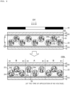
- the irradiation with the active energy ray is performed through the photomask 40 under the state in which a voltage is applied between the first transparent conductive film 10 and the second transparent conductive film 30.
- the polymerizable liquid crystal compound 24b is polymerized under the state of being aligned in a predetermined direction (in the illustrated example, in a direction perpendicular to the main surfaces of the transparent conductive films 10 and 30 ) along an electric field in each of the liquid crystal droplets 24 of the irradiated region of the PDLC layer 20, and hence the liquid crystal polymer 24c in which the alignment is fixed is formed.
- a PDLC film which is in a scattering state on the entirety of a surface at the time of application of no voltage, and which exhibits such an appearance that a haze is continuously increased from a right end portion to a left end portion at the time of application of a voltage, can be obtained.
- a PDLC film which is in a transparent state on the entirety of a surface at the time of application of a voltage, and which exhibits such an appearance that a haze is continuously decreased from a right end portion to a left end portion at the time of application of no voltage, can be obtained.
- the volume-average particle diameter was calculated by: setting the aperture size to 30 ⁇ m; and dividing the measured values into 256 sections arranged at equal intervals in the range of from 0.6 um to 18 um on a logarithmic scale to collect the statistics of volumes for each discretized particle diameter.
- An ITO layer was formed on one surface of a PET substrate (thickness: 50 um) by a sputtering method to provide a transparent conductive film having the configuration [transparent substrate/transparent electrode layer].
- the above-mentioned emulsion application liquid was applied to the ITO layer surface of the first transparent conductive film to form an applied layer having a thickness of 20 um.
- the application was performed with a slot die, and a line speed was 6 m/min.
- the applied layer was dried at 25°C for 8 minutes to form a PDLC layer having a thickness of 8 um.
- the second transparent conductive film was laminated on the above-mentioned PDLC layer so that its ITO layer faced the PDLC layer.
- a PDLC film was obtained.
Landscapes
- Physics & Mathematics (AREA)
- Nonlinear Science (AREA)
- Chemical & Material Sciences (AREA)
- Crystallography & Structural Chemistry (AREA)
- General Physics & Mathematics (AREA)
- Optics & Photonics (AREA)
- Mathematical Physics (AREA)
- Dispersion Chemistry (AREA)
- Liquid Crystal (AREA)
- Manufacture Of Macromolecular Shaped Articles (AREA)
Applications Claiming Priority (2)
| Application Number | Priority Date | Filing Date | Title |
|---|---|---|---|
| JP2021142442A JP7776281B2 (ja) | 2021-09-01 | 2021-09-01 | 高分子分散型液晶フィルムおよび高分子分散型液晶フィルムの製造方法 |
| PCT/JP2022/031088 WO2023032675A1 (ja) | 2021-09-01 | 2022-08-17 | 高分子分散型液晶フィルムおよび高分子分散型液晶フィルムの製造方法 |
Publications (2)
| Publication Number | Publication Date |
|---|---|
| EP4398026A1 true EP4398026A1 (de) | 2024-07-10 |
| EP4398026A4 EP4398026A4 (de) | 2025-08-13 |
Family
ID=85411133
Family Applications (1)
| Application Number | Title | Priority Date | Filing Date |
|---|---|---|---|
| EP22864260.9A Withdrawn EP4398026A4 (de) | 2021-09-01 | 2022-08-17 | Polymerdispersions-flüssigkristallfolie und verfahren zur herstellung einer polymerdispersions-flüssigkristallfolie |
Country Status (7)
| Country | Link |
|---|---|
| US (1) | US20240402530A1 (de) |
| EP (1) | EP4398026A4 (de) |
| JP (1) | JP7776281B2 (de) |
| KR (1) | KR20240054271A (de) |
| CN (1) | CN117897653A (de) |
| TW (1) | TW202317378A (de) |
| WO (1) | WO2023032675A1 (de) |
Cited By (1)
| Publication number | Priority date | Publication date | Assignee | Title |
|---|---|---|---|---|
| WO2026080453A1 (en) * | 2024-10-08 | 2026-04-16 | Carbon, Inc. | Methods of additive manufacturing with liquid crystalline build surfaces |
Families Citing this family (7)
| Publication number | Priority date | Publication date | Assignee | Title |
|---|---|---|---|---|
| JP2023145004A (ja) * | 2022-03-28 | 2023-10-11 | 日東電工株式会社 | 高分子分散型液晶フィルムおよび高分子分散型液晶フィルムの製造方法 |
| JP7834625B2 (ja) * | 2022-09-28 | 2026-03-24 | 日東電工株式会社 | 高分子分散型液晶フィルム |
| JP2024143490A (ja) * | 2023-03-30 | 2024-10-11 | 日東電工株式会社 | 拡散フィルム、光拡散装置、液晶表示装置、および拡散フィルムの製造方法 |
| JP2024145373A (ja) * | 2023-03-31 | 2024-10-15 | 日東電工株式会社 | 光拡散装置、バックライト装置、および画像表示装置 |
| JP2025059712A (ja) * | 2023-09-29 | 2025-04-10 | 日東電工株式会社 | 拡散フィルムおよび光拡散装置 |
| JP2025059711A (ja) * | 2023-09-29 | 2025-04-10 | 日東電工株式会社 | 高分子分散型液晶フィルム |
| CN119148421B (zh) * | 2024-09-18 | 2025-09-02 | 北京大学 | 一种具有智能信息加密功能的液晶薄膜及其制备方法和应用 |
Family Cites Families (22)
| Publication number | Priority date | Publication date | Assignee | Title |
|---|---|---|---|---|
| DE3119459A1 (de) | 1981-05-15 | 1982-12-09 | Consortium für elektrochemische Industrie GmbH, 8000 München | Fluessig-kristalline eigenschaften aufweisende, vernetzte organopolysiloxane |
| EP0261712A1 (de) | 1986-09-04 | 1988-03-30 | Koninklijke Philips Electronics N.V. | Bildanzeigezelle, Verfahren zur Herstellung einer orientierenden Schicht über ein Substrat dieser Bildanzeigezelle und Monomer-Verbindung für ihre Anwendung als orientierende Schicht |
| DE3830592A1 (de) | 1988-09-08 | 1990-04-12 | Consortium Elektrochem Ind | (meth)acryloxygruppen enthaltende fluessigkristalline polyorganosiloxane |
| JPH04355719A (ja) | 1991-06-03 | 1992-12-09 | Nippon Sheet Glass Co Ltd | 液晶素子の製造方法 |
| WO1993022397A1 (en) | 1992-04-27 | 1993-11-11 | Merck Patent Gmbh | Electrooptical liquid crystal system |
| GB2280445B (en) | 1993-07-05 | 1998-02-11 | Merck Patent Gmbh | Liquid crystalline copolymer |
| DE19504224A1 (de) | 1994-02-23 | 1995-08-24 | Merck Patent Gmbh | Flüssigkristallines Material |
| DE4408171A1 (de) | 1994-03-11 | 1995-09-14 | Basf Ag | Neue polymerisierbare flüssigkristalline Verbindungen |
| JP3273164B2 (ja) * | 1996-10-23 | 2002-04-08 | 松下電器産業株式会社 | 液晶パネルの製造方法及びその製造装置 |
| JP2000214443A (ja) * | 1998-11-20 | 2000-08-04 | Matsushita Electric Ind Co Ltd | 液晶表示素子およびその製造方法 |
| DE19859584A1 (de) | 1998-12-22 | 2000-06-29 | Basf Ag | Verwendung polymerisierbarer flüssigkristalliner Substanzen zur Herstellung optischer Bauelemente |
| JP2002189123A (ja) | 2000-12-19 | 2002-07-05 | Hitachi Chem Co Ltd | 調光材料、調光フィルム及び調光フィルムの製造方法 |
| US8801964B2 (en) * | 2010-12-22 | 2014-08-12 | Photon Dynamics, Inc. | Encapsulated polymer network liquid crystal material, device and applications |
| JP6115955B2 (ja) | 2013-08-22 | 2017-04-19 | 国立研究開発法人産業技術総合研究所 | 液晶分散液の製造方法 |
| CA3018343A1 (en) * | 2016-03-23 | 2017-09-28 | Guardian Glass, LLC | Low haze switchable liquid crystal arrangement for use in switchable window or the like |
| WO2018020333A1 (en) * | 2016-07-29 | 2018-02-01 | Semiconductor Energy Laboratory Co., Ltd. | Separation method, display device, display module, and electronic device |
| JP7019315B2 (ja) | 2017-06-23 | 2022-02-15 | 日東電工株式会社 | 調光フィルムの製造方法 |
| JP7275580B2 (ja) * | 2019-01-04 | 2023-05-18 | 凸版印刷株式会社 | 調光装置、および、調光シート |
| CN109713559B (zh) * | 2019-02-01 | 2020-06-12 | 中国科学院理化技术研究所 | 一种蓝相液晶膜及其制备方法和用途 |
| KR20220062042A (ko) * | 2019-09-09 | 2022-05-13 | 메르크 파텐트 게엠베하 | 액정 매질 및 pnlc 광 변조 소자 |
| CN112327522B (zh) * | 2020-11-04 | 2023-04-07 | Tcl华星光电技术有限公司 | 温度响应的液晶薄膜及其制备方法和应用 |
| CN113126371B (zh) * | 2021-04-26 | 2023-03-31 | 上海天马微电子有限公司 | 一种调光装置及其制作方法 |
-
2021
- 2021-09-01 JP JP2021142442A patent/JP7776281B2/ja active Active
-
2022
- 2022-08-17 KR KR1020247006008A patent/KR20240054271A/ko active Pending
- 2022-08-17 EP EP22864260.9A patent/EP4398026A4/de not_active Withdrawn
- 2022-08-17 US US18/688,416 patent/US20240402530A1/en active Pending
- 2022-08-17 WO PCT/JP2022/031088 patent/WO2023032675A1/ja not_active Ceased
- 2022-08-17 CN CN202280058751.1A patent/CN117897653A/zh active Pending
- 2022-08-26 TW TW111132253A patent/TW202317378A/zh unknown
Cited By (1)
| Publication number | Priority date | Publication date | Assignee | Title |
|---|---|---|---|---|
| WO2026080453A1 (en) * | 2024-10-08 | 2026-04-16 | Carbon, Inc. | Methods of additive manufacturing with liquid crystalline build surfaces |
Also Published As
| Publication number | Publication date |
|---|---|
| KR20240054271A (ko) | 2024-04-25 |
| CN117897653A (zh) | 2024-04-16 |
| TW202317378A (zh) | 2023-05-01 |
| JP7776281B2 (ja) | 2025-11-26 |
| WO2023032675A1 (ja) | 2023-03-09 |
| EP4398026A4 (de) | 2025-08-13 |
| JP2023035529A (ja) | 2023-03-13 |
| US20240402530A1 (en) | 2024-12-05 |
Similar Documents
| Publication | Publication Date | Title |
|---|---|---|
| EP4398026A1 (de) | Polymerdispersions-flüssigkristallfolie und verfahren zur herstellung einer polymerdispersions-flüssigkristallfolie | |
| KR20140093765A (ko) | 투명 도전성 필름, 터치 패널 및 표시 장치 | |
| KR20090104061A (ko) | 광학 적층 필름 | |
| KR20150111929A (ko) | 반사 방지 필름 및 그 제조 방법 | |
| KR20150112965A (ko) | 반사 방지 필름 및 그 제조 방법 | |
| TW202346100A (zh) | 高分子分散型液晶膜及高分子分散型液晶膜之製造方法 | |
| KR20160001688A (ko) | 편광판 보호 필름, 편광판, 화상 표시 장치, 및 편광판 보호 필름의 제조 방법 | |
| US20250199354A1 (en) | Optical film and method for producing optical film | |
| US12111530B2 (en) | Polymer-dispersed-type liquid crystal film, emulsion, and method for producing polymer-dispersed-type liquid crystal film | |
| US20240219764A1 (en) | Polymer dispersed liquid crystal film and manufacturing method therefor | |
| JP2013092782A (ja) | 光学積層体 | |
| JP7478722B2 (ja) | 透過型スクリーンおよび映像表示装置 | |
| US20250216714A1 (en) | Polymer-dispersed liquid crystal film, optical film set, and method for producing polymer-dispersed liquid crystal film | |
| WO2025069525A1 (ja) | 高分子分散型液晶フィルム | |
| JP7834625B2 (ja) | 高分子分散型液晶フィルム | |
| US20260110932A1 (en) | Polymer dispersion-type liquid crystal film | |
| KR20250139752A (ko) | 광학 필름 및 백라이트 장치 | |
| JP2008256757A (ja) | 光学積層体 |
Legal Events
| Date | Code | Title | Description |
|---|---|---|---|
| STAA | Information on the status of an ep patent application or granted ep patent |
Free format text: STATUS: THE INTERNATIONAL PUBLICATION HAS BEEN MADE |
|
| PUAI | Public reference made under article 153(3) epc to a published international application that has entered the european phase |
Free format text: ORIGINAL CODE: 0009012 |
|
| STAA | Information on the status of an ep patent application or granted ep patent |
Free format text: STATUS: REQUEST FOR EXAMINATION WAS MADE |
|
| 17P | Request for examination filed |
Effective date: 20240228 |
|
| AK | Designated contracting states |
Kind code of ref document: A1 Designated state(s): AL AT BE BG CH CY CZ DE DK EE ES FI FR GB GR HR HU IE IS IT LI LT LU LV MC MK MT NL NO PL PT RO RS SE SI SK SM TR |
|
| DAV | Request for validation of the european patent (deleted) | ||
| DAX | Request for extension of the european patent (deleted) | ||
| A4 | Supplementary search report drawn up and despatched |
Effective date: 20250716 |
|
| RIC1 | Information provided on ipc code assigned before grant |
Ipc: G02F 1/1334 20060101AFI20250710BHEP Ipc: G02F 1/13 20060101ALI20250710BHEP Ipc: G02F 1/137 20060101ALI20250710BHEP |
|
| STAA | Information on the status of an ep patent application or granted ep patent |
Free format text: STATUS: THE APPLICATION HAS BEEN WITHDRAWN |
|
| 18W | Application withdrawn |
Effective date: 20250919 |