EP4398039A1 - Appareil de traitement de substrat - Google Patents
Appareil de traitement de substrat Download PDFInfo
- Publication number
- EP4398039A1 EP4398039A1 EP23740004.9A EP23740004A EP4398039A1 EP 4398039 A1 EP4398039 A1 EP 4398039A1 EP 23740004 A EP23740004 A EP 23740004A EP 4398039 A1 EP4398039 A1 EP 4398039A1
- Authority
- EP
- European Patent Office
- Prior art keywords
- substrate
- speed
- mask
- exposure
- coating
- Prior art date
- Legal status (The legal status is an assumption and is not a legal conclusion. Google has not performed a legal analysis and makes no representation as to the accuracy of the status listed.)
- Pending
Links
Images


Classifications
-
- G—PHYSICS
- G03—PHOTOGRAPHY; CINEMATOGRAPHY; ANALOGOUS TECHNIQUES USING WAVES OTHER THAN OPTICAL WAVES; ELECTROGRAPHY; HOLOGRAPHY
- G03F—PHOTOMECHANICAL PRODUCTION OF TEXTURED OR PATTERNED SURFACES, e.g. FOR PRINTING, FOR PROCESSING OF SEMICONDUCTOR DEVICES; MATERIALS THEREFOR; ORIGINALS THEREFOR; APPARATUS SPECIALLY ADAPTED THEREFOR
- G03F7/00—Photomechanical, e.g. photolithographic, production of textured or patterned surfaces, e.g. printing surfaces; Materials therefor, e.g. comprising photoresists; Apparatus specially adapted therefor
- G03F7/16—Coating processes; Apparatus therefor
-
- G—PHYSICS
- G03—PHOTOGRAPHY; CINEMATOGRAPHY; ANALOGOUS TECHNIQUES USING WAVES OTHER THAN OPTICAL WAVES; ELECTROGRAPHY; HOLOGRAPHY
- G03F—PHOTOMECHANICAL PRODUCTION OF TEXTURED OR PATTERNED SURFACES, e.g. FOR PRINTING, FOR PROCESSING OF SEMICONDUCTOR DEVICES; MATERIALS THEREFOR; ORIGINALS THEREFOR; APPARATUS SPECIALLY ADAPTED THEREFOR
- G03F7/00—Photomechanical, e.g. photolithographic, production of textured or patterned surfaces, e.g. printing surfaces; Materials therefor, e.g. comprising photoresists; Apparatus specially adapted therefor
- G03F7/70—Microphotolithographic exposure; Apparatus therefor
- G03F7/708—Construction of apparatus, e.g. environment aspects, hygiene aspects or materials
- G03F7/70991—Connection with other apparatus, e.g. multiple exposure stations, particular arrangement of exposure apparatus and pre-exposure and/or post-exposure apparatus; Shared apparatus, e.g. having shared radiation source, shared mask or workpiece stage, shared base-plate; Utilities, e.g. cable, pipe or wireless arrangements for data, power, fluids or vacuum
-
- B—PERFORMING OPERATIONS; TRANSPORTING
- B08—CLEANING
- B08B—CLEANING IN GENERAL; PREVENTION OF FOULING IN GENERAL
- B08B3/00—Cleaning by methods involving the use or presence of liquid or steam
- B08B3/02—Cleaning by the force of jets or sprays
-
- C—CHEMISTRY; METALLURGY
- C25—ELECTROLYTIC OR ELECTROPHORETIC PROCESSES; APPARATUS THEREFOR
- C25F—PROCESSES FOR THE ELECTROLYTIC REMOVAL OF MATERIALS FROM OBJECTS; APPARATUS THEREFOR
- C25F3/00—Electrolytic etching or polishing
- C25F3/02—Etching
- C25F3/14—Etching locally
-
- G—PHYSICS
- G03—PHOTOGRAPHY; CINEMATOGRAPHY; ANALOGOUS TECHNIQUES USING WAVES OTHER THAN OPTICAL WAVES; ELECTROGRAPHY; HOLOGRAPHY
- G03F—PHOTOMECHANICAL PRODUCTION OF TEXTURED OR PATTERNED SURFACES, e.g. FOR PRINTING, FOR PROCESSING OF SEMICONDUCTOR DEVICES; MATERIALS THEREFOR; ORIGINALS THEREFOR; APPARATUS SPECIALLY ADAPTED THEREFOR
- G03F7/00—Photomechanical, e.g. photolithographic, production of textured or patterned surfaces, e.g. printing surfaces; Materials therefor, e.g. comprising photoresists; Apparatus specially adapted therefor
- G03F7/16—Coating processes; Apparatus therefor
- G03F7/162—Coating on a rotating support, e.g. using a whirler or a spinner
-
- G—PHYSICS
- G03—PHOTOGRAPHY; CINEMATOGRAPHY; ANALOGOUS TECHNIQUES USING WAVES OTHER THAN OPTICAL WAVES; ELECTROGRAPHY; HOLOGRAPHY
- G03F—PHOTOMECHANICAL PRODUCTION OF TEXTURED OR PATTERNED SURFACES, e.g. FOR PRINTING, FOR PROCESSING OF SEMICONDUCTOR DEVICES; MATERIALS THEREFOR; ORIGINALS THEREFOR; APPARATUS SPECIALLY ADAPTED THEREFOR
- G03F7/00—Photomechanical, e.g. photolithographic, production of textured or patterned surfaces, e.g. printing surfaces; Materials therefor, e.g. comprising photoresists; Apparatus specially adapted therefor
- G03F7/16—Coating processes; Apparatus therefor
- G03F7/168—Finishing the coated layer, e.g. drying, baking, soaking
-
- G—PHYSICS
- G03—PHOTOGRAPHY; CINEMATOGRAPHY; ANALOGOUS TECHNIQUES USING WAVES OTHER THAN OPTICAL WAVES; ELECTROGRAPHY; HOLOGRAPHY
- G03F—PHOTOMECHANICAL PRODUCTION OF TEXTURED OR PATTERNED SURFACES, e.g. FOR PRINTING, FOR PROCESSING OF SEMICONDUCTOR DEVICES; MATERIALS THEREFOR; ORIGINALS THEREFOR; APPARATUS SPECIALLY ADAPTED THEREFOR
- G03F7/00—Photomechanical, e.g. photolithographic, production of textured or patterned surfaces, e.g. printing surfaces; Materials therefor, e.g. comprising photoresists; Apparatus specially adapted therefor
- G03F7/20—Exposure; Apparatus therefor
- G03F7/2002—Exposure; Apparatus therefor with visible light or UV light, through an original having an opaque pattern on a transparent support, e.g. film printing, projection printing; by reflection of visible or UV light from an original such as a printed image
- G03F7/201—Exposure; Apparatus therefor with visible light or UV light, through an original having an opaque pattern on a transparent support, e.g. film printing, projection printing; by reflection of visible or UV light from an original such as a printed image characterised by an oblique exposure; characterised by the use of plural sources; characterised by the rotation of the optical device; characterised by a relative movement of the optical device, the light source, the sensitive system or the mask
-
- G—PHYSICS
- G03—PHOTOGRAPHY; CINEMATOGRAPHY; ANALOGOUS TECHNIQUES USING WAVES OTHER THAN OPTICAL WAVES; ELECTROGRAPHY; HOLOGRAPHY
- G03F—PHOTOMECHANICAL PRODUCTION OF TEXTURED OR PATTERNED SURFACES, e.g. FOR PRINTING, FOR PROCESSING OF SEMICONDUCTOR DEVICES; MATERIALS THEREFOR; ORIGINALS THEREFOR; APPARATUS SPECIALLY ADAPTED THEREFOR
- G03F7/00—Photomechanical, e.g. photolithographic, production of textured or patterned surfaces, e.g. printing surfaces; Materials therefor, e.g. comprising photoresists; Apparatus specially adapted therefor
- G03F7/20—Exposure; Apparatus therefor
- G03F7/2022—Multi-step exposure, e.g. hybrid; backside exposure; blanket exposure, e.g. for image reversal; edge exposure, e.g. for edge bead removal; corrective exposure
- G03F7/2032—Simultaneous exposure of the front side and the backside
-
- G—PHYSICS
- G03—PHOTOGRAPHY; CINEMATOGRAPHY; ANALOGOUS TECHNIQUES USING WAVES OTHER THAN OPTICAL WAVES; ELECTROGRAPHY; HOLOGRAPHY
- G03F—PHOTOMECHANICAL PRODUCTION OF TEXTURED OR PATTERNED SURFACES, e.g. FOR PRINTING, FOR PROCESSING OF SEMICONDUCTOR DEVICES; MATERIALS THEREFOR; ORIGINALS THEREFOR; APPARATUS SPECIALLY ADAPTED THEREFOR
- G03F7/00—Photomechanical, e.g. photolithographic, production of textured or patterned surfaces, e.g. printing surfaces; Materials therefor, e.g. comprising photoresists; Apparatus specially adapted therefor
- G03F7/20—Exposure; Apparatus therefor
- G03F7/2035—Exposure; Apparatus therefor simultaneous coating and exposure; using a belt mask, e.g. endless
-
- G—PHYSICS
- G03—PHOTOGRAPHY; CINEMATOGRAPHY; ANALOGOUS TECHNIQUES USING WAVES OTHER THAN OPTICAL WAVES; ELECTROGRAPHY; HOLOGRAPHY
- G03F—PHOTOMECHANICAL PRODUCTION OF TEXTURED OR PATTERNED SURFACES, e.g. FOR PRINTING, FOR PROCESSING OF SEMICONDUCTOR DEVICES; MATERIALS THEREFOR; ORIGINALS THEREFOR; APPARATUS SPECIALLY ADAPTED THEREFOR
- G03F7/00—Photomechanical, e.g. photolithographic, production of textured or patterned surfaces, e.g. printing surfaces; Materials therefor, e.g. comprising photoresists; Apparatus specially adapted therefor
- G03F7/26—Processing photosensitive materials; Apparatus therefor
- G03F7/42—Stripping or agents therefor
- G03F7/422—Stripping or agents therefor using liquids only
-
- G—PHYSICS
- G03—PHOTOGRAPHY; CINEMATOGRAPHY; ANALOGOUS TECHNIQUES USING WAVES OTHER THAN OPTICAL WAVES; ELECTROGRAPHY; HOLOGRAPHY
- G03F—PHOTOMECHANICAL PRODUCTION OF TEXTURED OR PATTERNED SURFACES, e.g. FOR PRINTING, FOR PROCESSING OF SEMICONDUCTOR DEVICES; MATERIALS THEREFOR; ORIGINALS THEREFOR; APPARATUS SPECIALLY ADAPTED THEREFOR
- G03F7/00—Photomechanical, e.g. photolithographic, production of textured or patterned surfaces, e.g. printing surfaces; Materials therefor, e.g. comprising photoresists; Apparatus specially adapted therefor
- G03F7/70—Microphotolithographic exposure; Apparatus therefor
- G03F7/70425—Imaging strategies, e.g. for increasing throughput or resolution, printing product fields larger than the image field or compensating lithography- or non-lithography errors, e.g. proximity correction, mix-and-match, stitching or double patterning
- G03F7/70433—Layout for increasing efficiency or for compensating imaging errors, e.g. layout of exposure fields for reducing focus errors; Use of mask features for increasing efficiency or for compensating imaging errors
-
- G—PHYSICS
- G03—PHOTOGRAPHY; CINEMATOGRAPHY; ANALOGOUS TECHNIQUES USING WAVES OTHER THAN OPTICAL WAVES; ELECTROGRAPHY; HOLOGRAPHY
- G03F—PHOTOMECHANICAL PRODUCTION OF TEXTURED OR PATTERNED SURFACES, e.g. FOR PRINTING, FOR PROCESSING OF SEMICONDUCTOR DEVICES; MATERIALS THEREFOR; ORIGINALS THEREFOR; APPARATUS SPECIALLY ADAPTED THEREFOR
- G03F7/00—Photomechanical, e.g. photolithographic, production of textured or patterned surfaces, e.g. printing surfaces; Materials therefor, e.g. comprising photoresists; Apparatus specially adapted therefor
- G03F7/70—Microphotolithographic exposure; Apparatus therefor
- G03F7/70425—Imaging strategies, e.g. for increasing throughput or resolution, printing product fields larger than the image field or compensating lithography- or non-lithography errors, e.g. proximity correction, mix-and-match, stitching or double patterning
- G03F7/70466—Multiple exposures, e.g. combination of fine and coarse exposures, double patterning or multiple exposures for printing a single feature
-
- G—PHYSICS
- G03—PHOTOGRAPHY; CINEMATOGRAPHY; ANALOGOUS TECHNIQUES USING WAVES OTHER THAN OPTICAL WAVES; ELECTROGRAPHY; HOLOGRAPHY
- G03F—PHOTOMECHANICAL PRODUCTION OF TEXTURED OR PATTERNED SURFACES, e.g. FOR PRINTING, FOR PROCESSING OF SEMICONDUCTOR DEVICES; MATERIALS THEREFOR; ORIGINALS THEREFOR; APPARATUS SPECIALLY ADAPTED THEREFOR
- G03F7/00—Photomechanical, e.g. photolithographic, production of textured or patterned surfaces, e.g. printing surfaces; Materials therefor, e.g. comprising photoresists; Apparatus specially adapted therefor
- G03F7/70—Microphotolithographic exposure; Apparatus therefor
- G03F7/70691—Handling of masks or workpieces
- G03F7/707—Chucks, e.g. chucking or un-chucking operations or structural details
-
- B—PERFORMING OPERATIONS; TRANSPORTING
- B08—CLEANING
- B08B—CLEANING IN GENERAL; PREVENTION OF FOULING IN GENERAL
- B08B2203/00—Details of cleaning machines or methods involving the use or presence of liquid or steam
- B08B2203/02—Details of machines or methods for cleaning by the force of jets or sprays
-
- H—ELECTRICITY
- H01—ELECTRIC ELEMENTS
- H01M—PROCESSES OR MEANS, e.g. BATTERIES, FOR THE DIRECT CONVERSION OF CHEMICAL ENERGY INTO ELECTRICAL ENERGY
- H01M4/00—Electrodes
- H01M4/02—Electrodes composed of, or comprising, active material
- H01M4/64—Carriers or collectors
- H01M4/70—Carriers or collectors characterised by shape or form
Definitions
- the material cannot continuously move at a uniform speed in the exposure device, so that the exposure device cannot be integrate with the coating device, the drying device and other devices.
- multiple separate devices are required for the processing of the current collector, which results in high equipment cost and cannot save on the time cost of transferring the current collector between the multiple devices, thus limiting the processing efficiency of the current collector.
- the current collector is processed by multiple separate devices, which cannot achieve high consistency.
- FIG. 1 shows a schematic structural diagram of a vehicle 1 according to the present application.
- the vehicle 1 may be a fuel vehicle, a gas vehicle or a new-energy vehicle.
- the new-energy vehicle may be a battery electric vehicle, a hybrid vehicle, an extended-range vehicle, etc.
- a motor 11, a controller 12 and a battery 10 may be provided inside the vehicle 1.
- the controller 12 is configured to control the battery 10 to supply power to the motor 11.
- the battery 10 may be arranged at the bottom, the front or the rear of the vehicle 1.
- the battery 10 may be configured to supply power to the vehicle 1.
- the battery 10 may serve as an operating power supply for the vehicle 1 for use in a circuit system of the vehicle 1 to meet, for example, the operating power demand during the startup, navigation and traveling of the vehicle 1.
- the battery 10 may not only serve as an operation power supply for the vehicle 1, but may also serve as a driving power supply for the vehicle 1, in place of or partially in place of fuel or natural gas, to supply driving power to the vehicle 1.
- a drying device 302 is configured to receive the substrate 30, which is coated by means of the coating device 301, at the first speed and dry the material.
- An etching device304 is configured to receive the substrate 30, which is exposed by means of the exposure device 303, at the first speed and etch the material and a portion of the substrate 30 in an unexposed region of the substrate.
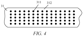
- FIG. 4 is a schematic structural diagram of a mask 31 according to an embodiment of the present application.
- the mask 31 has light-shielding portions 311 and a light-transmitting portion 312, and the light-shielding portions 311 and/or the light-transmitting portion 312 constitute an exposure pattern on the mask 31.
- the apparatus 300 further includes a feeding device 305 configured to convey the substrate 30 at the first speed in the feeding direction.
- the feeding device 305 in this embodiment of the present application is of, for example, but not limited to, a roll-to-roll structure.
- the feeding device 305 may also be in the form of a clamping and feeding mechanism having a manipulator, etc.
- the cleaning device 306 uses a combined structure of the spray rod 3061 and the cleaning tank 3062, and can quickly clean the etched substrate 30 to remove the residual material, etching liquid and other contaminants from the surface of the substrate 30, so that the apparatus 300 outputs the substrate 30 that can be directly used.
- the coating device 301 is also provided with a coating roller 3012.
- the coating roller 3012 is located between the two feeding rollers of the first feeding module 3011, and is configured to coat the substrate 30 in the vertical state with the material.
- the surface of the coating roller 3012 has a textured structure, the coating roller 3012 is partially immersed in a material tray, and during coating, the coating roller 3012 rotates to move the material such that the material passes through a flexible scraper and is then taken away by the reversely moving substrate 30 so as to coat the substrate 30 with a layer of material.
- the drying device 302 includes multiple heating tubes 3021 and multiple air knives 3022.
- the multiple heating tubes 3021 and multiple air knives 3022 are disposed at intervals on the two sides of the substrate 30 in the feeding direction.
- the arrangement of the multiple heating tubes 3021 and the multiple air knives 3022 at intervals means that, on each side of the substrate 30, the heating tubes 3021 and the air knives 3022 are spaced apart from each other, with one air knife 3022 being provided between two adjacent heating tubes 3021, and one heating tube 3021 being provided between two adjacent air knives 3022. It should be understood that, in some other embodiments, the number and arrangement of the heating tubes 3021 and the air knives 3022 can be configured according to the drying speed, feeding speed, etc. required for processing the substrate 30. For example, three heating tubes 3021 are provided between two adjacent air knives 3022.
- the material coated on the substrate 30 can be quickly dried for pre-curing of the material, and the substrate 30 does not need to stay in the drying device 302, so that the drying device 302 can cooperate with other devices to allow the substrate 30 to always travel at the same feeding speed in the feeding direction, which facilitates integration of the apparatus 300.
- the exposure device303 includes a mask conveying module 3031.
- the mask conveying module 3031 is configured to continuously convey the mask 31 at the first speed in the feeding direction.
- the exposure device 303 can perform continuous processing of a complex pattern, which improves the operation efficiency and performance of the exposure device 303 and is thus conducive to improving the efficiency and performance of the apparatus 300.
- the mask 31 is a strip-shaped mask
- the mask conveying module 3031 is configured to convey the strip-shaped mask to the exposure region at the first speed.
- the strip-shaped mask 31 may be conveyed in a roll-to-roll manner, so as to keep the mask 31 to move synchronously with the substrate 30 in the exposure region through a release and recovery process similar to that of the substrate 30. This will not be described herein again.
- the endless mask 31 is supported by the first drive roller 3031a and the driven roller 3031b provided on the inside to form a closed structure, and the first drive roller 3031a and the driven roller 3031b form a cyclic driving mechanism, so that the endless mask 31 can rotate in circles as the first drive roller 3031a and the driven roller 3031b rotate, and the endless mask 31 with the pattern can pass through the exposure region and then be rotated to the exposure region again.
- the mask conveying module 3031 rotates the mask 31 by means of the structure of the drive roller 3031a and the driven roller 3031b, and can control the movement conditions of the mask 31 by means of controlling the rotation speed and rotation direction of the drive roller 3031a and fix the movement path of the mask 31 by means of the driven roller 3031b, so as to achieve flexible control of the mask 31 to improve the flexibility of the exposure device 303, which is conducive to improving the treatment performance of the substrate treatment apparatus 300.
- the etching device 304 includes a conductive roller 3041, a first electrode 3042 and an etching tank 3043.
- the conductive roller 3041 and the first electrode 3042 are disposed in the etching tank 3043, and the etching tank 3043 holds an electrolyte solution.
- the conductive roller 3041 and the first electrode 3042 have opposite polarities, and the conductive roller 3041 comes into contact with the exposed substrate 30 and conveys the substrate 30 to the etching tank 3043 at the first speed.
- multiple first electrodes 3042 may be provided and disposed in the etching tank 3043 and close to the substrate 30.
- the conductive roller 3041 and the first electrode 3042 with opposite polarities form a cathode and an anode in a dielectric solution.
- the substrate 30 is a current collector, and the portions of the current collector that are not coated with photoresist will be etched so as to form a corresponding pattern or through hole.
- the electrochemical etching is taken as a specific example, but in some other embodiments, the etching device 304 may also use physical etching, dry etching, etc. to etch the substrate.
Landscapes
- Physics & Mathematics (AREA)
- General Physics & Mathematics (AREA)
- Engineering & Computer Science (AREA)
- Chemical & Material Sciences (AREA)
- Organic Chemistry (AREA)
- Electrochemistry (AREA)
- Materials Engineering (AREA)
- Metallurgy (AREA)
- Chemical Kinetics & Catalysis (AREA)
- Computer Networks & Wireless Communication (AREA)
- Health & Medical Sciences (AREA)
- Environmental & Geological Engineering (AREA)
- Epidemiology (AREA)
- Public Health (AREA)
- Manufacturing Of Printed Circuit Boards (AREA)
- Coating Apparatus (AREA)
Applications Claiming Priority (2)
| Application Number | Priority Date | Filing Date | Title |
|---|---|---|---|
| CN202220092551.5U CN217181402U (zh) | 2022-01-14 | 2022-01-14 | 一种基材处理的设备 |
| PCT/CN2023/071530 WO2023134662A1 (fr) | 2022-01-14 | 2023-01-10 | Appareil de traitement de substrat |
Publications (2)
| Publication Number | Publication Date |
|---|---|
| EP4398039A1 true EP4398039A1 (fr) | 2024-07-10 |
| EP4398039A4 EP4398039A4 (fr) | 2025-10-22 |
Family
ID=82736121
Family Applications (1)
| Application Number | Title | Priority Date | Filing Date |
|---|---|---|---|
| EP23740004.9A Pending EP4398039A4 (fr) | 2022-01-14 | 2023-01-10 | Appareil de traitement de substrat |
Country Status (4)
| Country | Link |
|---|---|
| US (1) | US20240272562A1 (fr) |
| EP (1) | EP4398039A4 (fr) |
| CN (1) | CN217181402U (fr) |
| WO (1) | WO2023134662A1 (fr) |
Families Citing this family (3)
| Publication number | Priority date | Publication date | Assignee | Title |
|---|---|---|---|---|
| CN116360219A (zh) * | 2021-12-21 | 2023-06-30 | 宁德时代新能源科技股份有限公司 | 曝光装置 |
| CN217181402U (zh) * | 2022-01-14 | 2022-08-12 | 宁德时代新能源科技股份有限公司 | 一种基材处理的设备 |
| CN115832498B (zh) * | 2022-11-24 | 2024-01-26 | 厦门海辰储能科技股份有限公司 | 一种电池电极的回收设备及回收方法 |
Family Cites Families (10)
| Publication number | Priority date | Publication date | Assignee | Title |
|---|---|---|---|---|
| JPS60205452A (ja) * | 1984-03-30 | 1985-10-17 | Canon Inc | 露光方法 |
| US9465296B2 (en) * | 2010-01-12 | 2016-10-11 | Rolith, Inc. | Nanopatterning method and apparatus |
| CN102323719B (zh) * | 2011-06-30 | 2014-09-03 | 丹阳博昱科技有限公司 | 一种连续曝光方法和装置 |
| KR20190141027A (ko) * | 2012-05-24 | 2019-12-20 | 가부시키가이샤 니콘 | 디바이스 제조 방법 |
| JP2013254113A (ja) * | 2012-06-07 | 2013-12-19 | Arisawa Mfg Co Ltd | 露光装置及び露光方法 |
| JP6702332B2 (ja) * | 2015-09-29 | 2020-06-03 | 株式会社ニコン | 製造システム |
| WO2020026957A1 (fr) * | 2018-07-31 | 2020-02-06 | 富士フイルム株式会社 | Plaque originale de plaque d'impression planographique, corps stratifié de plaque originale de plaque d'impression planographique, procédé de fabrication de plaque pour plaque d'impression planographique, et procédé d'impression planographique |
| CN111712046B (zh) * | 2020-06-29 | 2021-04-09 | 江苏软讯科技有限公司 | 一种通过辊涂和光罩结合制作高分辨率导电图案的方法 |
| CN214766615U (zh) * | 2020-12-30 | 2021-11-19 | 上海兰钧新能源科技有限公司 | 一种涂布装置 |
| CN217181402U (zh) * | 2022-01-14 | 2022-08-12 | 宁德时代新能源科技股份有限公司 | 一种基材处理的设备 |
-
2022
- 2022-01-14 CN CN202220092551.5U patent/CN217181402U/zh active Active
-
2023
- 2023-01-10 WO PCT/CN2023/071530 patent/WO2023134662A1/fr not_active Ceased
- 2023-01-10 EP EP23740004.9A patent/EP4398039A4/fr active Pending
-
2024
- 2024-04-24 US US18/644,211 patent/US20240272562A1/en active Pending
Also Published As
| Publication number | Publication date |
|---|---|
| US20240272562A1 (en) | 2024-08-15 |
| CN217181402U (zh) | 2022-08-12 |
| EP4398039A4 (fr) | 2025-10-22 |
| WO2023134662A1 (fr) | 2023-07-20 |
Similar Documents
| Publication | Publication Date | Title |
|---|---|---|
| EP4398039A1 (fr) | Appareil de traitement de substrat | |
| KR101204539B1 (ko) | 에너지 저장 장치의 전극 제조용 도핑 장치 및 이를 이용한 전극 제조 방법 | |
| KR101204598B1 (ko) | 에너지 저장 장치의 전극 제조용 도핑 장치 및 이를 이용한 전극 제조 방법 | |
| US20130302674A1 (en) | Battery electrode and a method for producing same | |
| WO2023128374A1 (fr) | Dispositif et procédé de traitement au laser | |
| CN217181403U (zh) | 一种曝光设备 | |
| JP2011198774A (ja) | 電気化学セル積層体の層を電気的に絶縁するための製造プロセスおよび装置 | |
| CN210224168U (zh) | 一种锂离子电池极片预锂化装置 | |
| KR102273330B1 (ko) | 2차 전지용 전극 생산 시스템의 스태킹 장치 | |
| US12492479B2 (en) | Etching device | |
| US20260051553A1 (en) | Material separation device for waste battery recycling and method therefor | |
| EP4706840A1 (fr) | Appareil de nettoyage de rouleau de laminage | |
| EP4443242A1 (fr) | Appareil d'exposition | |
| KR102903643B1 (ko) | 전극 건조장치 | |
| JP2025527449A (ja) | 電極の圧延ロール洗浄方法および洗浄装置 | |
| US20260021602A1 (en) | Complex facility and facility layout | |
| KR20260056640A (ko) | 배터리 셀 제조장치 및 제조방법 | |
| KR102771652B1 (ko) | 레이저 노칭 장치 | |
| KR100343793B1 (ko) | 이차 전지의 집전체 제조 장치와, 이를 이용한 집전체제조 방법 | |
| KR102891247B1 (ko) | 전극 건조장치 | |
| KR102891244B1 (ko) | 이차전지 전극 제조 시스템 | |
| US20250026597A1 (en) | Automatic Separator Supply Apparatus | |
| WO2024242225A1 (fr) | Appareil de séchage d'électrode | |
| KR20250053318A (ko) | 전극 제조장치 및 이를 이용한 전극 제조방법 | |
| WO2025150932A1 (fr) | Appareil de fabrication de batterie secondaire et procédé de fabrication de batterie secondaire |
Legal Events
| Date | Code | Title | Description |
|---|---|---|---|
| STAA | Information on the status of an ep patent application or granted ep patent |
Free format text: STATUS: THE INTERNATIONAL PUBLICATION HAS BEEN MADE |
|
| PUAI | Public reference made under article 153(3) epc to a published international application that has entered the european phase |
Free format text: ORIGINAL CODE: 0009012 |
|
| STAA | Information on the status of an ep patent application or granted ep patent |
Free format text: STATUS: REQUEST FOR EXAMINATION WAS MADE |
|
| 17P | Request for examination filed |
Effective date: 20240403 |
|
| AK | Designated contracting states |
Kind code of ref document: A1 Designated state(s): AL AT BE BG CH CY CZ DE DK EE ES FI FR GB GR HR HU IE IS IT LI LT LU LV MC ME MK MT NL NO PL PT RO RS SE SI SK SM TR |
|
| RAP1 | Party data changed (applicant data changed or rights of an application transferred) |
Owner name: CONTEMPORARY AMPEREX TECHNOLOGY(HONG KONG) LIMITED |
|
| DAV | Request for validation of the european patent (deleted) | ||
| DAX | Request for extension of the european patent (deleted) | ||
| REG | Reference to a national code |
Ref country code: DE Ref legal event code: R079 Free format text: PREVIOUS MAIN CLASS: G03F0007420000 Ipc: G03F0007200000 |
|
| RIC1 | Information provided on ipc code assigned before grant |
Ipc: G03F 7/20 20060101AFI20250626BHEP Ipc: G03F 7/16 20060101ALI20250626BHEP Ipc: G03F 7/42 20060101ALI20250626BHEP |
|
| A4 | Supplementary search report drawn up and despatched |
Effective date: 20250924 |
|
| RIC1 | Information provided on ipc code assigned before grant |
Ipc: G03F 7/20 20060101AFI20250918BHEP Ipc: G03F 7/16 20060101ALI20250918BHEP Ipc: G03F 7/42 20060101ALI20250918BHEP |