EP4398048A2 - Tragbare elektronische vorrichtung und montageverfahren - Google Patents
Tragbare elektronische vorrichtung und montageverfahren Download PDFInfo
- Publication number
- EP4398048A2 EP4398048A2 EP24177178.1A EP24177178A EP4398048A2 EP 4398048 A2 EP4398048 A2 EP 4398048A2 EP 24177178 A EP24177178 A EP 24177178A EP 4398048 A2 EP4398048 A2 EP 4398048A2
- Authority
- EP
- European Patent Office
- Prior art keywords
- bio
- signal
- electronic device
- unit
- cover
- Prior art date
- Legal status (The legal status is an assumption and is not a legal conclusion. Google has not performed a legal analysis and makes no representation as to the accuracy of the status listed.)
- Granted
Links
Images




Classifications
-
- A—HUMAN NECESSITIES
- A61—MEDICAL OR VETERINARY SCIENCE; HYGIENE
- A61B—DIAGNOSIS; SURGERY; IDENTIFICATION
- A61B5/00—Measuring for diagnostic purposes; Identification of persons
- A61B5/0002—Remote monitoring of patients using telemetry, e.g. transmission of vital signals via a communication network
- A61B5/0015—Remote monitoring of patients using telemetry, e.g. transmission of vital signals via a communication network characterised by features of the telemetry system
-
- A—HUMAN NECESSITIES
- A61—MEDICAL OR VETERINARY SCIENCE; HYGIENE
- A61B—DIAGNOSIS; SURGERY; IDENTIFICATION
- A61B5/00—Measuring for diagnostic purposes; Identification of persons
- A61B5/0059—Measuring for diagnostic purposes; Identification of persons using light, e.g. diagnosis by transillumination, diascopy, fluorescence
-
- A—HUMAN NECESSITIES
- A61—MEDICAL OR VETERINARY SCIENCE; HYGIENE
- A61B—DIAGNOSIS; SURGERY; IDENTIFICATION
- A61B5/00—Measuring for diagnostic purposes; Identification of persons
- A61B5/24—Detecting, measuring or recording bioelectric or biomagnetic signals of the body or parts thereof
- A61B5/25—Bioelectric electrodes therefor
- A61B5/251—Means for maintaining electrode contact with the body
- A61B5/256—Wearable electrodes, e.g. having straps or bands
-
- A—HUMAN NECESSITIES
- A61—MEDICAL OR VETERINARY SCIENCE; HYGIENE
- A61B—DIAGNOSIS; SURGERY; IDENTIFICATION
- A61B5/00—Measuring for diagnostic purposes; Identification of persons
- A61B5/24—Detecting, measuring or recording bioelectric or biomagnetic signals of the body or parts thereof
- A61B5/25—Bioelectric electrodes therefor
- A61B5/279—Bioelectric electrodes therefor specially adapted for particular uses
- A61B5/28—Bioelectric electrodes therefor specially adapted for particular uses for electrocardiography [ECG]
- A61B5/282—Holders for multiple electrodes
-
- A—HUMAN NECESSITIES
- A61—MEDICAL OR VETERINARY SCIENCE; HYGIENE
- A61B—DIAGNOSIS; SURGERY; IDENTIFICATION
- A61B5/00—Measuring for diagnostic purposes; Identification of persons
- A61B5/24—Detecting, measuring or recording bioelectric or biomagnetic signals of the body or parts thereof
- A61B5/316—Modalities, i.e. specific diagnostic methods
- A61B5/318—Heart-related electrical modalities, e.g. electrocardiography [ECG]
- A61B5/339—Displays specially adapted therefor
-
- A—HUMAN NECESSITIES
- A61—MEDICAL OR VETERINARY SCIENCE; HYGIENE
- A61B—DIAGNOSIS; SURGERY; IDENTIFICATION
- A61B5/00—Measuring for diagnostic purposes; Identification of persons
- A61B5/68—Arrangements of detecting, measuring or recording means, e.g. sensors, in relation to patient
- A61B5/6801—Arrangements of detecting, measuring or recording means, e.g. sensors, in relation to patient specially adapted to be attached to or worn on the body surface
- A61B5/6802—Sensor mounted on worn items
- A61B5/681—Wristwatch-type devices
-
- A—HUMAN NECESSITIES
- A61—MEDICAL OR VETERINARY SCIENCE; HYGIENE
- A61B—DIAGNOSIS; SURGERY; IDENTIFICATION
- A61B5/00—Measuring for diagnostic purposes; Identification of persons
- A61B5/72—Signal processing specially adapted for physiological signals or for diagnostic purposes
- A61B5/7221—Determining signal validity, reliability or quality
-
- G—PHYSICS
- G04—HOROLOGY
- G04G—ELECTRONIC TIME-PIECES
- G04G17/00—Structural details; Housings
- G04G17/02—Component assemblies
- G04G17/04—Mounting of electronic components
-
- G—PHYSICS
- G04—HOROLOGY
- G04G—ELECTRONIC TIME-PIECES
- G04G17/00—Structural details; Housings
- G04G17/02—Component assemblies
- G04G17/06—Electric connectors, e.g. conductive elastomers
-
- G—PHYSICS
- G04—HOROLOGY
- G04G—ELECTRONIC TIME-PIECES
- G04G21/00—Input or output devices integrated in time-pieces
- G04G21/02—Detectors of external physical values, e.g. temperature
- G04G21/025—Detectors of external physical values, e.g. temperature for measuring physiological data
-
- G—PHYSICS
- G06—COMPUTING OR CALCULATING; COUNTING
- G06F—ELECTRIC DIGITAL DATA PROCESSING
- G06F1/00—Details not covered by groups G06F3/00 - G06F13/00 and G06F21/00
- G06F1/16—Constructional details or arrangements
- G06F1/1613—Constructional details or arrangements for portable computers
- G06F1/163—Wearable computers, e.g. on a belt
-
- G—PHYSICS
- G06—COMPUTING OR CALCULATING; COUNTING
- G06F—ELECTRIC DIGITAL DATA PROCESSING
- G06F1/00—Details not covered by groups G06F3/00 - G06F13/00 and G06F21/00
- G06F1/16—Constructional details or arrangements
- G06F1/1613—Constructional details or arrangements for portable computers
- G06F1/1633—Constructional details or arrangements of portable computers not specific to the type of enclosures covered by groups G06F1/1615 - G06F1/1626
- G06F1/1635—Details related to the integration of battery packs and other power supplies such as fuel cells or integrated AC adapter
-
- G—PHYSICS
- G06—COMPUTING OR CALCULATING; COUNTING
- G06F—ELECTRIC DIGITAL DATA PROCESSING
- G06F1/00—Details not covered by groups G06F3/00 - G06F13/00 and G06F21/00
- G06F1/16—Constructional details or arrangements
- G06F1/1613—Constructional details or arrangements for portable computers
- G06F1/1633—Constructional details or arrangements of portable computers not specific to the type of enclosures covered by groups G06F1/1615 - G06F1/1626
- G06F1/1656—Details related to functional adaptations of the enclosure, e.g. to provide protection against EMI, shock, water, or to host detachable peripherals like a mouse or removable expansions units like PCMCIA cards, or to provide access to internal components for maintenance or to removable storage supports like CDs or DVDs, or to mechanically mount accessories
-
- G—PHYSICS
- G06—COMPUTING OR CALCULATING; COUNTING
- G06F—ELECTRIC DIGITAL DATA PROCESSING
- G06F1/00—Details not covered by groups G06F3/00 - G06F13/00 and G06F21/00
- G06F1/16—Constructional details or arrangements
- G06F1/1613—Constructional details or arrangements for portable computers
- G06F1/1633—Constructional details or arrangements of portable computers not specific to the type of enclosures covered by groups G06F1/1615 - G06F1/1626
- G06F1/1656—Details related to functional adaptations of the enclosure, e.g. to provide protection against EMI, shock, water, or to host detachable peripherals like a mouse or removable expansions units like PCMCIA cards, or to provide access to internal components for maintenance or to removable storage supports like CDs or DVDs, or to mechanically mount accessories
- G06F1/1658—Details related to functional adaptations of the enclosure, e.g. to provide protection against EMI, shock, water, or to host detachable peripherals like a mouse or removable expansions units like PCMCIA cards, or to provide access to internal components for maintenance or to removable storage supports like CDs or DVDs, or to mechanically mount accessories related to the mounting of internal components, e.g. disc drive or any other functional module
-
- G—PHYSICS
- G06—COMPUTING OR CALCULATING; COUNTING
- G06F—ELECTRIC DIGITAL DATA PROCESSING
- G06F1/00—Details not covered by groups G06F3/00 - G06F13/00 and G06F21/00
- G06F1/16—Constructional details or arrangements
- G06F1/1613—Constructional details or arrangements for portable computers
- G06F1/1633—Constructional details or arrangements of portable computers not specific to the type of enclosures covered by groups G06F1/1615 - G06F1/1626
- G06F1/1684—Constructional details or arrangements related to integrated I/O peripherals not covered by groups G06F1/1635 - G06F1/1675
-
- G—PHYSICS
- G06—COMPUTING OR CALCULATING; COUNTING
- G06F—ELECTRIC DIGITAL DATA PROCESSING
- G06F1/00—Details not covered by groups G06F3/00 - G06F13/00 and G06F21/00
- G06F1/16—Constructional details or arrangements
- G06F1/1613—Constructional details or arrangements for portable computers
- G06F1/1633—Constructional details or arrangements of portable computers not specific to the type of enclosures covered by groups G06F1/1615 - G06F1/1626
- G06F1/1684—Constructional details or arrangements related to integrated I/O peripherals not covered by groups G06F1/1635 - G06F1/1675
- G06F1/1698—Constructional details or arrangements related to integrated I/O peripherals not covered by groups G06F1/1635 - G06F1/1675 the I/O peripheral being a sending/receiving arrangement to establish a cordless communication link, e.g. radio or infrared link, integrated cellular phone
-
- G—PHYSICS
- G06—COMPUTING OR CALCULATING; COUNTING
- G06F—ELECTRIC DIGITAL DATA PROCESSING
- G06F1/00—Details not covered by groups G06F3/00 - G06F13/00 and G06F21/00
- G06F1/26—Power supply means, e.g. regulation thereof
- G06F1/263—Arrangements for using multiple switchable power supplies, e.g. battery and AC
-
- H—ELECTRICITY
- H02—GENERATION; CONVERSION OR DISTRIBUTION OF ELECTRIC POWER
- H02J—ELECTRIC POWER NETWORKS; CIRCUIT ARRANGEMENTS OR SYSTEMS FOR SUPPLYING OR DISTRIBUTING ELECTRIC POWER; SYSTEMS FOR STORING ELECTRIC ENERGY
- H02J50/00—Circuit arrangements or systems for wireless supply or distribution of electric power
- H02J50/10—Circuit arrangements or systems for wireless supply or distribution of electric power using inductive coupling
-
- A—HUMAN NECESSITIES
- A61—MEDICAL OR VETERINARY SCIENCE; HYGIENE
- A61B—DIAGNOSIS; SURGERY; IDENTIFICATION
- A61B2562/00—Details of sensors; Constructional details of sensor housings or probes; Accessories for sensors
- A61B2562/16—Details of sensor housings or probes; Details of structural supports for sensors
- A61B2562/164—Details of sensor housings or probes; Details of structural supports for sensors the sensor is mounted in or on a conformable substrate or carrier
-
- A—HUMAN NECESSITIES
- A61—MEDICAL OR VETERINARY SCIENCE; HYGIENE
- A61B—DIAGNOSIS; SURGERY; IDENTIFICATION
- A61B2562/00—Details of sensors; Constructional details of sensor housings or probes; Accessories for sensors
- A61B2562/16—Details of sensor housings or probes; Details of structural supports for sensors
- A61B2562/166—Details of sensor housings or probes; Details of structural supports for sensors the sensor is mounted on a specially adapted printed circuit board
-
- A—HUMAN NECESSITIES
- A61—MEDICAL OR VETERINARY SCIENCE; HYGIENE
- A61B—DIAGNOSIS; SURGERY; IDENTIFICATION
- A61B2562/00—Details of sensors; Constructional details of sensor housings or probes; Accessories for sensors
- A61B2562/18—Shielding or protection of sensors from environmental influences, e.g. protection from mechanical damage
- A61B2562/185—Optical shielding, e.g. baffles
Definitions
- Various embodiments disclosed herein relate to a wearable electronic device and a method for assembling the same.
- Wearable electronic devices worn on users' bodies have gradually diversified functions. Moreover, wearable electronic devices have gradually decreased sizes.
- wearable electronic devices In line with increasing interests in good health, wearable electronic devices have been equipped with functions for measuring users' biometric information. Wristwatch-type wearable electronic devices have recently been equipped with various sensors including heartbeat sensors.
- PCB printed circuit board
- FPCB flexible printed circuit board
- An electronic device may include a display, a processor operatively connected to the display, a cover facing the display and having at least a portion formed of a light-transmitting material, a flexible printed circuit board having a first surface facing the cover, and a second surface corresponding to an opposite surface of the first surface, a wireless charging coil disposed so as to surround the flexible printed circuit board, a first bio-signal sensing unit including a light-receiving unit and a light-emitting unit mounted on the first surface of the flexible printed circuit board, a second bio-signal sensing unit including an internal electrode formed inside the cover, corresponding to a portion facing the flexible printed circuit board, and an external electrode electrically connected to the internal electrode and formed outside the cover, a contact unit having one end mounted on the first surface of the flexible printed circuit board, extending to the cover so that the opposite end thereof is connected to the internal electrode of the second bio-signal sensing unit, and a signal processing unit mounted on the second surface of the flexible printed circuit board to
- An assembly method may include disposing a wireless charging coil having a ring shape on a cover, and disposing a flexible printed circuit board on the inner circumference of the wireless charging coil, wherein in the disposing of the flexible printed circuit board, a contact unit is brought into contact with an internal electrode formed on the cover such that the contact unit extends to the cover with one end of the contact unit mounted on the flexible printed circuit board.
- FIG. 1 is a block diagram illustrating an electronic device 101 in a network environment 100 according to various embodiments.
- the electronic device 101 in the network environment 100 may communicate with an electronic device 102 via a first network 198 (e.g., a short-range wireless communication network), or an electronic device 104 or a server 108 via a second network 199 (e.g., a long-range wireless communication network).
- the electronic device 101 may communicate with the electronic device 104 via the server 108.
- the processor 120 may include a main processor 121 (e.g., a central processing unit (CPU) or an application processor (AP)), and an auxiliary processor 123 (e.g., a graphics processing unit (GPU), an image signal processor (ISP), a sensor hub processor, or a communication processor (CP)) that is operable independently from, or in conjunction with, the main processor 121.
- auxiliary processor 123 may be adapted to consume less power than the main processor 121, or to be specific to a specified function.
- the auxiliary processor 123 may be implemented as separate from, or as part of the main processor 121.
- the program 140 may be stored in the memory 130 as software, and may include, for example, an operating system (OS) 142, middleware 144, or an application 146.
- OS operating system
- middleware middleware
- application application
- the display device 160 may visually provide information to the outside (e.g., a user) of the electronic device 101.
- the display device 160 may include, for example, a display, a hologram device, or a projector and control circuitry to control a corresponding one of the display, hologram device, and projector.
- the display device 160 may include touch circuitry adapted to detect a touch, or sensor circuitry (e.g., a pressure sensor) adapted to measure the intensity of force incurred by the touch.
- the audio module 170 may convert a sound into an electrical signal and vice versa. According to an embodiment, the audio module 170 may obtain the sound via the input device 150, or output the sound via the sound output device 155 or a headphone of an external electronic device (e.g., an electronic device 102) directly (e.g., wiredly) or wirelessly coupled with the electronic device 101.
- an external electronic device e.g., an electronic device 102
- directly e.g., wiredly
- wirelessly e.g., wirelessly
- the sensor module 176 may detect an operational state (e.g., power or temperature) of the electronic device 101 or an environmental state (e.g., a state of a user) external to the electronic device 101, and then generate an electrical signal or data value corresponding to the detected state.
- the sensor module 176 may include, for example, a gesture sensor, a gyro sensor, an atmospheric pressure sensor, a magnetic sensor, an acceleration sensor, a grip sensor, a proximity sensor, a color sensor, an infrared (IR) sensor, a biometric sensor, a temperature sensor, a humidity sensor, or an illuminance sensor.
- the power management module 188 may manage power supplied to the electronic device 101.
- the power management module 188 may be implemented as at least part of, for example, a power management integrated circuit (PMIC).
- PMIC power management integrated circuit
- the battery 189 may supply power to at least one component of the electronic device 101.
- the battery 189 may include, for example, a primary cell which is not rechargeable, a secondary cell which is rechargeable, or a fuel cell.
- the communication module 190 may include a wireless communication module 192 (e.g., a cellular communication module, a short-range wireless communication module, or a global navigation satellite system (GNSS) communication module) or a wired communication module 194 (e.g., a local area network (LAN) communication module or a power line communication (PLC) module).
- a wireless communication module 192 e.g., a cellular communication module, a short-range wireless communication module, or a global navigation satellite system (GNSS) communication module
- GNSS global navigation satellite system
- wired communication module 194 e.g., a local area network (LAN) communication module or a power line communication (PLC) module.
- LAN local area network
- PLC power line communication
- the antenna module 197 may transmit or receive a signal or power to or from the outside (e.g., the external electronic device) of the electronic device 101.
- the antenna module 197 may include an antenna including a radiating element composed of a conductive material or a conductive pattern formed in or on a substrate (e.g., PCB).
- the antenna module 197 may include a plurality of antennas. In such a case, at least one antenna appropriate for a communication scheme used in the communication network, such as the first network 198 or the second network 199, may be selected, for example, by the communication module 190 (e.g., the wireless communication module 192) from the plurality of antennas.
- the signal or the power may then be transmitted or received between the communication module 190 and the external electronic device via the selected at least one antenna.
- another component e.g., a radio frequency integrated circuit (RFIC)
- RFIC radio frequency integrated circuit
- At least some of the above-described components may be coupled mutually and communicate signals (e.g., commands or data) therebetween via an inter-peripheral communication scheme (e.g., a bus, general purpose input and output (GPIO), serial peripheral interface (SPI), or mobile industry processor interface (MIPI)).
- an inter-peripheral communication scheme e.g., a bus, general purpose input and output (GPIO), serial peripheral interface (SPI), or mobile industry processor interface (MIPI)
- the coupling member 250 and 260 may be detachably coupled to at least a portion of the housing 210 by using a locking member 251 and 261.
- the coupling member 250 and 260 may include one or more of a fixation member 252, a fixation member fastening hole 253, a band guide member 254, and a band fixation ring 255.
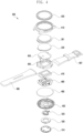
- the first bio-signal sensing unit 540, the contact unit 560, and the signal processing unit 570 mounted to the flexible printed circuit board 520 and the second bio-signal sensing unit 550 mounted to the cover 510 may constitute a sensor module (e.g.: sensor module 211 in FIG. 3 ).
- the second bio-signal sensing unit 550 may sense a second bio-signal and include an internal electrode 551 and 552 and an external electrode 553 and 554.
- the second bio-signal sensed by the second bio-signal sensing unit 550 may include a bio-signal related to an electrocardiogram of a user.
- a bio-signal related to an electrocardiogram of a user may include a bio-signal related to an electrocardiogram of a user.
- an operation of sensing the second bio-signal by the second bio-signal sensing unit 550 including the external electrode 553 and 554 and the internal electrode 551 and 552 will be described in brief.
- the second bio-signal sensing unit 550 may sense an electrocardiogram-related signal by sensing an electrical signal upon myocardial contraction.
- an action potential spreads from the heart throughout the body.
- the potential difference generated by the current caused by the contraction or relaxation of the myocardium can be obtained.
- such a potential difference may be obtained by using the first external electrode 553 of the second bio-signal sensing unit 550 and an electrocardiogram electrode of an external electronic device.
- the electronic device according to various embodiments disclosed herein is an electronic device mounted on a wrist, the first external electrode 553 may be in contact with a wrist of a user.
- the sensing of the second bio-signal of the second bio-signal sensing unit 550 described above explains the representative principle of obtaining electrocardiogram-related information by using multiple electrodes, and the second bio-signal sensing unit 550 according to various embodiments disclosed herein may obtain the electrocardiogram-related information as the second bio-signal using various other methods in addition thereto.
- one end of the contact unit 560 may be mounted on the first surface of the flexible printed circuit board 520.
- the other end of the contact unit 560 may be in contact with the internal electrode 551 and 552 of the second bio-signal sensing unit 550.
- the contact unit 560 may include a conductive material.
- the contact unit 560 may be connected to the internal electrode 551 and 552 of the second bio-signal sensing unit 550 so as to electrically connect the internal electrode 551 and 552 to the flexible printed circuit board 520.
- the contact unit 560 may extend in a direction perpendicular to the first surface of the flexible printed circuit board 520.
- the second magnet 583 may be disposed on the second surface of the flexible printed circuit board 520.
- the space in which the second magnet 583 is disposed may be a space formed by the signal processing unit 570 mounted on the second surface of the flexible printed circuit board 520.
- the volume of the signal processing unit 570 itself may form a space corresponding to the height of the signal processing unit 570 between the flexible printed circuit board 520 and a component in contact with the flexible printed circuit board 520.
- the second magnet 583 may be disposed in this space.
- the central axis of the first magnet 581 may be aligned with the central axis of the second magnet 583.
- the first magnet 581 and the second magnet 583 may fix and connect the electronic device according to various embodiments disclosed herein to a charging device.
- the electronic device may include a wireless charging coil 530.
- the wireless charging coil 530 of the electronic device When the wireless charging coil 530 of the electronic device is disposed within a configured range in relation to a charging coil of a charging device, the electronic device may be charged wirelessly by the charging device.
- the charging device may include a magnet therein. The relative positions of the first magnet 581 and the second magnet 583, and the wireless charging coil 530 in the electronic device are determined. Likewise, the relative positions of the magnet of the charging device and the charging coil of the charging device are determined.
- the volume of the magnet needs to be a certain level or more.
- the electronic device may ensure sufficient mounting conformability and mounting force through the first magnet 581 and the second magnet 583 disposed on opposite surfaces of the flexible printed circuit board 520.
- the second magnet 583 is disposed in a space formed by the signal processing unit 570, and thus the electronic device may minimize the space receiving the first magnet 581 and the second magnet 583.
- An optically shielding member 590 may optically shield between the first magnet 581 and the cover 510.
- the light-emitting unit 541 of the first bio-signal sensing unit 540 may be disposed at the center of the first magnet 581.
- the light generated from the light-emitting unit 541 should not leak between the first magnet 581 and the cover 510. This is because the light-receiving unit 543 needs to receive only the light reflected from the body of a user.
- the optically shielding member 590 may be installed on one of the first magnet 581 and the cover 510 between the first magnet 581 and the cover 510 to shield between the first magnet 581 and the cover 510 such that the light-emitting unit 541 is optically shielded.
- FIG. 8 is a planar view of the cover 510 illustrated in FIG. 5 .
- an optical film 800 may be attached to the inner surface of the cover 510.
- the optical film 800 may be a film having a polarization attribute.
- the optical film 800 may prevent a component disposed in the electronic device from being seen from the outside through the cover 510.
- the optical film 800 may be formed in a circular shape as a whole.
- the optical film 800 may have two grooves 810 extending from a portion of the outer circumference thereof to the center of the optical film 800.
- the first internal electrode 551 and a second internal electrode 552 disposed on the cover 510 may be exposed through the two grooves 810.
- Two contact units 560 may be in contact with each of the first internal electrode 551 and the second internal electrode 552 exposed through the grooves 810 of the optical film 800.
- FIG. 9 is an operation flow chart illustrating a wearable electronic device detecting a bio-signal according to various embodiments disclosed herein.
- a processor e.g.: processor 120 in FIG. 1
- a processor of the electronic device may cause a first bio-signal sensing unit 540 to sense a first bio-signal (910).
- a user may input a command for sensing the first bio-signal through a touch input unit included in a display (e.g.: display 220 in FIG. 4 ) of the electronic device.
- the touch input unit may include a capacitive touch sensor or a pressure touch sensor to sense a user's touch input.
- the processor may cause the first bio-signal sensing unit 540 to sense the first bio-signal according to the command for sensing the first bio-signal.
- a user's command for sensing the first bio-signal may be input through an external electronic device wirelessly connected to the wearable electronic device.
- the command input through the external electronic device for sensing the first bio-signal may be received through a communication module included in the wearable electronic device.
- the processor may cause the first bio-signal sensing unit 540 to sense the first bio-signal according to the command received through the communication module for sensing the first bio-signal.
- the processor may cause the first bio-signal sensing unit 540 to sense the first bio-signal through various methods.
- the processor may compare the first bio-signal sensed by the first bio-signal sensing unit 540 with a predetermined value (920).
- the first bio-signal may include a bio-signal related to a cardiac impulse of a user.
- the predetermined value may include information on a cardiac impulse in a normal state. Cardiac impulse information in a normal state may be different depending on personal information such as age and gender. Cardiac impulse information in a normal state may be received from a server configured to provide related information and stored. In some cases, it is possible that the first bio-signal of a user in a normal state is used as the predetermined value.
- the processor checks whether a difference between the first bio-signal sensed by the first bio-signal sensing unit 540 and the predetermined value is within a range value (930). When the difference is out of the range value, the processor causes the second bio-signal sensing unit 550 to sense the second bio-signal (940). According to various embodiments, in case in which the difference between the sensed first bio-signal and the predetermined value is not within the range value, it is possible to display, on a display of the electronic device, that the sensed first bio-signal is not normal. Through this, it is possible to inform a user that the first bio-signal is out of the normal range.
- the second bio-signal may include a bio-signal related to electrocardiogram.
- the user may more efficiently and accurately measure his or her health conditions.
- FIG. 10 is a view illustrating an assembly method according to various embodiments disclosed herein.
- the wireless charging coil 530 having a ring shape may be disposed inside the cover 510.
- the flexible printed circuit board 520 may be disposed on the inner circumferential surface of the wireless charging coil 530.
- the contact unit 560 mounted on the first surface of the flexible printed circuit board 520 will to be disposed in contact with the internal electrode 551 and 552 of the cover 510.
- the internal electrode 551 and 552 of the cover 510 may be electrically connected to the flexible printed circuit board 520 through the contact unit 560 protruding toward the first surface of the flexible printed circuit board 520. Therefore, in a state in which the internal electrode 551 and 552 of the cover 510 and the contact unit 560 of the flexible printed circuit board 520 are aligned to each other, the internal electrode 551 and 552 and the flexible printed circuit board 520 may be easily connected just by arranging the flexible printed circuit board 520 on the cover 510. As a result, it is possible to have the effect of eliminating the risk of assembly defects and reducing the assembly cost.
- An electronic device may include: a display; a processor operatively connected to the display; a cover which faces the display and of which at least a part is formed of a light transmitting material; a flexible printed circuit board having a first side facing the cover, and a second side corresponding to the opposite side of the first side; a coil for wireless charging disposed to surround the flexible printed circuit board; a first bio-signal sensing unit including a light-emitting unit and a light-receiving unit mounted on the first side of the flexible printed circuit board; a second bio-signal sensing unit including an internal electrode formed inside the cover, which is a portion facing the flexible printed circuit board, and an external electrode electrically connected to the internal electrode and formed outside the cover; a contact unit having one end mounted on the first side of the flexible printed circuit board and extending to the cover such that the opposite end thereof is connected to the internal electrode of the second bio-signal sensing unit; and a signal processing unit mounted on the second side of the flexible
- the contact may be configured to extend in a direction perpendicular to the first surface of the flexible printed circuit board.
- a first magnet disposed on the first surface of the flexible printed circuit board may be further included.
- a second magnet disposed on the second surface of the flexible printed circuit board to be positioned in a space formed by the installation of the signal processing unit on the flexible printed circuit board may be further included.
- the first magnet may be configured to be in a ring shape to have the light-emitting unit of the first bio-signal sensing unit disposed at the center thereof.
- multiple light-receiving units of the first bio-signal sensing unit are arranged along the outer circumference of the first magnet.
- the external electrode may include a first external electrode and a second external electrode
- the internal electrode of the second bio-signal sensing unit may include a first internal electrode electrically connected to the first external electrode and a second internal electrode electrically connected to the second external electrode
- two of the contact units may be provided to be connected to the first internal electrode and the second internal electrode, respectively.
- an optical film attached to the cover may be further included.
- the optical film may be formed in a circular shape and have multiple grooves extending from a portion of the outer circumference toward the center thereof, and the first internal electrode and the second internal electrode of the internal electrode of the second bio-signal sensing unit may be arranged in the multiple grooves formed on the optical film, respectively.
- the processor may control the first bio-signal sensing unit to periodically sense a first bio-signal, check a difference between the first bio-signal sensed by the first bio-signal sensing unit and a predetermined value, and when the difference is out of a range value, cause the second bio-signal sensing unit to sense a second bio-signal.
- the processor may check a difference between the first bio-signal sensed by the first bio-signal sensing unit and a predetermined value, and when the difference is out of a range value, display, on a display of the electronic device, that the sensed first bio-signal is not normal.
- the processor may control the first bio-signal sensing unit to sense a first bio-signal, based on a touch input input through the display, check a difference between the first bio-signal sensed by the first bio-signal sensing unit and a predetermined value, and when the difference is out of a range value, cause the second bio-signal sensing unit to sense a second bio-signal.
- Operations for assembling an electronic device may include disposing a wireless charging coil having a ring shape on a cover; and disposing a flexible printed circuit board on the inner circumference of the wireless charging coil.
- the disposing the flexible printed circuit board causes one end of a contact unit to be mounted on the flexible printed circuit board and extend to the cover so as to be in contact with an internal electrode formed on the cover.
Landscapes
- Engineering & Computer Science (AREA)
- Health & Medical Sciences (AREA)
- Life Sciences & Earth Sciences (AREA)
- Physics & Mathematics (AREA)
- Computer Hardware Design (AREA)
- Theoretical Computer Science (AREA)
- General Engineering & Computer Science (AREA)
- General Physics & Mathematics (AREA)
- Biophysics (AREA)
- General Health & Medical Sciences (AREA)
- Human Computer Interaction (AREA)
- Animal Behavior & Ethology (AREA)
- Heart & Thoracic Surgery (AREA)
- Medical Informatics (AREA)
- Molecular Biology (AREA)
- Surgery (AREA)
- Biomedical Technology (AREA)
- Pathology (AREA)
- Public Health (AREA)
- Veterinary Medicine (AREA)
- Power Engineering (AREA)
- Cardiology (AREA)
- Computer Networks & Wireless Communication (AREA)
- Physiology (AREA)
- Artificial Intelligence (AREA)
- Computer Vision & Pattern Recognition (AREA)
- Psychiatry (AREA)
- Signal Processing (AREA)
- Measuring Pulse, Heart Rate, Blood Pressure Or Blood Flow (AREA)
- Measurement And Recording Of Electrical Phenomena And Electrical Characteristics Of The Living Body (AREA)
- Telephone Set Structure (AREA)
- User Interface Of Digital Computer (AREA)
Applications Claiming Priority (3)
| Application Number | Priority Date | Filing Date | Title |
|---|---|---|---|
| KR1020190093809A KR102771193B1 (ko) | 2019-08-01 | 2019-08-01 | 웨어러블 전자 장치 및 조립 방법 |
| EP20847421.3A EP3979038B1 (de) | 2019-08-01 | 2020-03-17 | Tragbare elektronische vorrichtung und montageverfahren |
| PCT/KR2020/003626 WO2021020687A1 (ko) | 2019-08-01 | 2020-03-17 | 웨어러블 전자 장치 및 조립 방법 |
Related Parent Applications (1)
| Application Number | Title | Priority Date | Filing Date |
|---|---|---|---|
| EP20847421.3A Division EP3979038B1 (de) | 2019-08-01 | 2020-03-17 | Tragbare elektronische vorrichtung und montageverfahren |
Publications (3)
| Publication Number | Publication Date |
|---|---|
| EP4398048A2 true EP4398048A2 (de) | 2024-07-10 |
| EP4398048A3 EP4398048A3 (de) | 2024-09-11 |
| EP4398048B1 EP4398048B1 (de) | 2025-07-02 |
Family
ID=74229222
Family Applications (2)
| Application Number | Title | Priority Date | Filing Date |
|---|---|---|---|
| EP24177178.1A Active EP4398048B1 (de) | 2019-08-01 | 2020-03-17 | Tragbare elektronische vorrichtung und montageverfahren |
| EP20847421.3A Active EP3979038B1 (de) | 2019-08-01 | 2020-03-17 | Tragbare elektronische vorrichtung und montageverfahren |
Family Applications After (1)
| Application Number | Title | Priority Date | Filing Date |
|---|---|---|---|
| EP20847421.3A Active EP3979038B1 (de) | 2019-08-01 | 2020-03-17 | Tragbare elektronische vorrichtung und montageverfahren |
Country Status (5)
| Country | Link |
|---|---|
| US (1) | US12226231B2 (de) |
| EP (2) | EP4398048B1 (de) |
| KR (1) | KR102771193B1 (de) |
| CN (1) | CN114207552B (de) |
| WO (1) | WO2021020687A1 (de) |
Families Citing this family (12)
| Publication number | Priority date | Publication date | Assignee | Title |
|---|---|---|---|---|
| US11803162B2 (en) * | 2020-09-25 | 2023-10-31 | Apple Inc. | Watch with sealed housing and sensor module |
| KR20220117613A (ko) * | 2021-02-17 | 2022-08-24 | 삼성전자주식회사 | 광학 센서를 고려한 후면 커버 구조를 포함하는 웨어러블 전자장치 |
| KR20220137198A (ko) * | 2021-04-01 | 2022-10-12 | 삼성전자주식회사 | 모듈 조립체를 포함하는 전자 장치 |
| KR102605607B1 (ko) * | 2021-11-05 | 2023-11-23 | (주)파트론 | Ppg 센서 패키지 |
| CN116196006A (zh) * | 2021-11-30 | 2023-06-02 | 荣耀终端有限公司 | 电子设备及生物电信号采集方法 |
| WO2023121405A1 (ko) * | 2021-12-24 | 2023-06-29 | 삼성전자 주식회사 | 센서 모듈을 포함하는 전자 장치 |
| CN116831538A (zh) * | 2022-03-23 | 2023-10-03 | 荣耀终端有限公司 | 可穿戴设备 |
| WO2023191330A1 (ko) * | 2022-03-29 | 2023-10-05 | 삼성전자 주식회사 | 복수의 전극 연결 구조를 포함하는 전자 장치 |
| EP4275599A4 (de) * | 2022-04-01 | 2025-04-09 | Samsung Electronics Co., Ltd. | Tragbare elektronische vorrichtung mit mehreren biometrischen sensoren |
| US12411549B2 (en) * | 2022-11-02 | 2025-09-09 | Meta Platforms Technologies, Llc | Wearable band structure having a band portion including embedded structural members with signal-processing components and another band portion not including any electrical components, and systems, devices, and methods of manufacturing thereof |
| CN116189544A (zh) * | 2023-03-15 | 2023-05-30 | 京东方科技集团股份有限公司 | 显示装置 |
| CN119170607A (zh) * | 2023-06-19 | 2024-12-20 | Jcet星科金朋韩国有限公司 | 半导体封装及其形成方法 |
Family Cites Families (19)
| Publication number | Priority date | Publication date | Assignee | Title |
|---|---|---|---|---|
| US20150102879A1 (en) | 2013-10-11 | 2015-04-16 | Olio Devices, Inc. | Wireless electronic device and method of use |
| WO2015126095A1 (ko) * | 2014-02-21 | 2015-08-27 | 삼성전자 주식회사 | 전자 장치 |
| CN105245019B (zh) * | 2014-07-07 | 2017-09-29 | 宏达国际电子股份有限公司 | 近场通讯及无线充电装置与其的切换方法 |
| KR20160044811A (ko) * | 2014-10-16 | 2016-04-26 | 삼성전자주식회사 | 생체 신호를 모니터링하는 웨어러블 센서 및 웨어러블 장치를 이용하여 생체 신호를 모니터링하는 방법 |
| KR20160054903A (ko) * | 2014-11-07 | 2016-05-17 | 엘지전자 주식회사 | 와치 타입 이동 단말기 |
| KR101670969B1 (ko) * | 2015-02-26 | 2016-11-10 | 한양대학교 에리카산학협력단 | 무선 충전 전자 기기의 인쇄회로기판 및 이를 이용한 무선 충전 전자 기기 |
| US9913591B2 (en) * | 2015-07-02 | 2018-03-13 | Verily Life Sciences Llc | Wrist-mounted device with integrated electronics |
| US10020668B2 (en) | 2015-07-27 | 2018-07-10 | Apple Inc. | Charging apparatus for wearable electronic device |
| US10424962B2 (en) * | 2015-09-30 | 2019-09-24 | Apple Inc. | Charging assembly for wireless power transfer |
| TWI610657B (zh) * | 2015-11-13 | 2018-01-11 | 慶旺科技股份有限公司 | 藉由心跳相關訊號評估個人心臟健康之穿戴式裝置及其訊號處理方法 |
| US10973422B2 (en) * | 2016-01-22 | 2021-04-13 | Fitbit, Inc. | Photoplethysmography-based pulse wave analysis using a wearable device |
| CN107041739A (zh) * | 2016-02-05 | 2017-08-15 | 光宝光电(常州)有限公司 | 穿戴式血压量测装置及其光学感测单元 |
| KR20170118439A (ko) | 2016-04-15 | 2017-10-25 | 삼성전자주식회사 | 생체 정보를 측정하는 전자 장치 및 그를 충전하는 장치 |
| KR20170141336A (ko) * | 2016-06-15 | 2017-12-26 | (주)에이치쓰리시스템 | 생체 신호 측정용 착용형 밴드 장치 |
| KR20180016866A (ko) * | 2016-08-08 | 2018-02-20 | 엘지전자 주식회사 | 와치타입 단말기 |
| KR102595232B1 (ko) * | 2016-09-23 | 2023-10-30 | 삼성전자주식회사 | 전자 장치에 있어서 무선 전력 송수신 장치 및 방법 |
| EP3415086A3 (de) | 2017-06-15 | 2019-04-03 | Analog Devices, Inc. | Sensormodul für lebenszeichenüberwachungsvorrichtung |
| KR101931100B1 (ko) * | 2017-06-19 | 2018-12-20 | 한국인터넷진흥원 | 생체신호를 이용한 멀티-모달형 웨어러블 사용자 인증 장치 |
| EP4470456A3 (de) * | 2017-09-26 | 2025-02-26 | Apple Inc. | Optisches sensorsubsystem neben einer abdeckung eines gehäuses einer elektronischen vorrichtung |
-
2019
- 2019-08-01 KR KR1020190093809A patent/KR102771193B1/ko active Active
-
2020
- 2020-03-17 EP EP24177178.1A patent/EP4398048B1/de active Active
- 2020-03-17 EP EP20847421.3A patent/EP3979038B1/de active Active
- 2020-03-17 WO PCT/KR2020/003626 patent/WO2021020687A1/ko not_active Ceased
- 2020-03-17 CN CN202080055158.2A patent/CN114207552B/zh active Active
-
2022
- 2022-01-31 US US17/589,461 patent/US12226231B2/en active Active
Also Published As
| Publication number | Publication date |
|---|---|
| EP4398048B1 (de) | 2025-07-02 |
| KR102771193B1 (ko) | 2025-02-24 |
| EP3979038A1 (de) | 2022-04-06 |
| WO2021020687A1 (ko) | 2021-02-04 |
| EP4398048A3 (de) | 2024-09-11 |
| US20220151554A1 (en) | 2022-05-19 |
| EP3979038B1 (de) | 2024-06-12 |
| US12226231B2 (en) | 2025-02-18 |
| CN114207552A (zh) | 2022-03-18 |
| EP3979038A4 (de) | 2022-08-17 |
| KR20210015250A (ko) | 2021-02-10 |
| CN114207552B (zh) | 2024-02-27 |
Similar Documents
| Publication | Publication Date | Title |
|---|---|---|
| US12226231B2 (en) | Wearable electronic device and assembly method | |
| KR102751068B1 (ko) | 안테나를 포함하는 와치형 전자 장치 | |
| US20190239769A1 (en) | Electronic device including detachable measurement module and attachment pad | |
| KR20210027785A (ko) | 생체 신호 측정용 전자 장치 | |
| US11759137B2 (en) | Electronic device for providing guide information | |
| US20230118495A1 (en) | Wearable electronic device including biometric sensor for measuring body temperature | |
| EP4387046A1 (de) | Elektronische vorrichtung mit spulenanordnung | |
| KR102819148B1 (ko) | 웨어러블 전자 장치 및 그에 적용되는 광학 필름 | |
| US11612348B2 (en) | Electronic device extending sensing area | |
| CN117177705A (zh) | 可穿戴电子装置 | |
| KR20200133456A (ko) | 포스 센서를 포함하는 웨어러블 전자 장치 | |
| KR20210107436A (ko) | 신체에 접촉되는 전극을 포함하는 전자 장치 | |
| US11051251B2 (en) | Hardware reset control method and electronic device | |
| KR20190114630A (ko) | 안테나를 포함하는 전자 장치 | |
| EP4292521A1 (de) | Sensorstruktur und elektronische vorrichtung mit der sensorstruktur | |
| US12399537B2 (en) | Electronic device for detecting moisture | |
| EP4351294A1 (de) | Elektronische vorrichtung mit elektrostatischem entladungspfad | |
| US12386318B2 (en) | Electronic device including biometric recognizing module | |
| EP4535122A1 (de) | Wearable-vorrichtung mit leiterplatte mit leitfähigem muster und elektronische vorrichtung | |
| KR20230085042A (ko) | 지문 센싱 방법 및 전자 장치 | |
| KR20250054663A (ko) | 복수의 스위치 소자를 포함하는 웨어러블 전자 장치 | |
| KR20250038559A (ko) | 다른 웨어러블 장치의 착용 상태를 식별하기 위한 웨어러블 전자 장치 및 방법 | |
| KR20240171967A (ko) | 웨어러블 전자 장치 | |
| KR20250035403A (ko) | 사용자의 생체 정보를 감지하기 위한 웨어러블 장치 | |
| KR20230114890A (ko) | 전기 영동 소자를 포함하는 웨어러블 전자 장치 |
Legal Events
| Date | Code | Title | Description |
|---|---|---|---|
| PUAI | Public reference made under article 153(3) epc to a published international application that has entered the european phase |
Free format text: ORIGINAL CODE: 0009012 |
|
| STAA | Information on the status of an ep patent application or granted ep patent |
Free format text: STATUS: THE APPLICATION HAS BEEN PUBLISHED |
|
| AC | Divisional application: reference to earlier application |
Ref document number: 3979038 Country of ref document: EP Kind code of ref document: P |
|
| AK | Designated contracting states |
Kind code of ref document: A2 Designated state(s): AL AT BE BG CH CY CZ DE DK EE ES FI FR GB GR HR HU IE IS IT LI LT LU LV MC MK MT NL NO PL PT RO RS SE SI SK SM TR |
|
| REG | Reference to a national code |
Ref country code: DE Ref legal event code: R079 Free format text: PREVIOUS MAIN CLASS: G04G0021020000 Ipc: G06F0001160000 Ref document number: 602020054074 Country of ref document: DE |
|
| PUAL | Search report despatched |
Free format text: ORIGINAL CODE: 0009013 |
|
| AK | Designated contracting states |
Kind code of ref document: A3 Designated state(s): AL AT BE BG CH CY CZ DE DK EE ES FI FR GB GR HR HU IE IS IT LI LT LU LV MC MK MT NL NO PL PT RO RS SE SI SK SM TR |
|
| RIC1 | Information provided on ipc code assigned before grant |
Ipc: G04G 21/02 20100101ALI20240805BHEP Ipc: G04G 17/06 20060101ALI20240805BHEP Ipc: G04G 17/04 20060101ALI20240805BHEP Ipc: A61B 5/024 20060101ALI20240805BHEP Ipc: A61B 5/00 20060101ALI20240805BHEP Ipc: G06F 1/26 20060101ALI20240805BHEP Ipc: G06F 1/16 20060101AFI20240805BHEP |
|
| STAA | Information on the status of an ep patent application or granted ep patent |
Free format text: STATUS: REQUEST FOR EXAMINATION WAS MADE |
|
| 17P | Request for examination filed |
Effective date: 20241203 |
|
| RBV | Designated contracting states (corrected) |
Designated state(s): AL AT BE BG CH CY CZ DE DK EE ES FI FR GB GR HR HU IE IS IT LI LT LU LV MC MK MT NL NO PL PT RO RS SE SI SK SM TR |
|
| GRAP | Despatch of communication of intention to grant a patent |
Free format text: ORIGINAL CODE: EPIDOSNIGR1 |
|
| STAA | Information on the status of an ep patent application or granted ep patent |
Free format text: STATUS: GRANT OF PATENT IS INTENDED |
|
| RIC1 | Information provided on ipc code assigned before grant |
Ipc: G04G 21/02 20100101ALI20250122BHEP Ipc: G04G 17/06 20060101ALI20250122BHEP Ipc: G04G 17/04 20060101ALI20250122BHEP Ipc: A61B 5/024 20060101ALI20250122BHEP Ipc: A61B 5/00 20060101ALI20250122BHEP Ipc: G06F 1/26 20060101ALI20250122BHEP Ipc: G06F 1/16 20060101AFI20250122BHEP |
|
| INTG | Intention to grant announced |
Effective date: 20250204 |
|
| GRAS | Grant fee paid |
Free format text: ORIGINAL CODE: EPIDOSNIGR3 |
|
| GRAA | (expected) grant |
Free format text: ORIGINAL CODE: 0009210 |
|
| STAA | Information on the status of an ep patent application or granted ep patent |
Free format text: STATUS: THE PATENT HAS BEEN GRANTED |
|
| AC | Divisional application: reference to earlier application |
Ref document number: 3979038 Country of ref document: EP Kind code of ref document: P |
|
| AK | Designated contracting states |
Kind code of ref document: B1 Designated state(s): AL AT BE BG CH CY CZ DE DK EE ES FI FR GB GR HR HU IE IS IT LI LT LU LV MC MK MT NL NO PL PT RO RS SE SI SK SM TR |
|
| REG | Reference to a national code |
Ref country code: GB Ref legal event code: FG4D |
|
| REG | Reference to a national code |
Ref country code: CH Ref legal event code: EP |
|
| REG | Reference to a national code |
Ref country code: DE Ref legal event code: R096 Ref document number: 602020054074 Country of ref document: DE |
|
| REG | Reference to a national code |
Ref country code: IE Ref legal event code: FG4D |
|
| REG | Reference to a national code |
Ref country code: NL Ref legal event code: MP Effective date: 20250702 |
|
| PG25 | Lapsed in a contracting state [announced via postgrant information from national office to epo] |
Ref country code: PT Free format text: LAPSE BECAUSE OF FAILURE TO SUBMIT A TRANSLATION OF THE DESCRIPTION OR TO PAY THE FEE WITHIN THE PRESCRIBED TIME-LIMIT Effective date: 20251103 |
|
| PG25 | Lapsed in a contracting state [announced via postgrant information from national office to epo] |
Ref country code: NL Free format text: LAPSE BECAUSE OF FAILURE TO SUBMIT A TRANSLATION OF THE DESCRIPTION OR TO PAY THE FEE WITHIN THE PRESCRIBED TIME-LIMIT Effective date: 20250702 |
|
| REG | Reference to a national code |
Ref country code: AT Ref legal event code: MK05 Ref document number: 1809947 Country of ref document: AT Kind code of ref document: T Effective date: 20250702 |
|
| PG25 | Lapsed in a contracting state [announced via postgrant information from national office to epo] |
Ref country code: IS Free format text: LAPSE BECAUSE OF FAILURE TO SUBMIT A TRANSLATION OF THE DESCRIPTION OR TO PAY THE FEE WITHIN THE PRESCRIBED TIME-LIMIT Effective date: 20251102 |
|
| PG25 | Lapsed in a contracting state [announced via postgrant information from national office to epo] |
Ref country code: NO Free format text: LAPSE BECAUSE OF FAILURE TO SUBMIT A TRANSLATION OF THE DESCRIPTION OR TO PAY THE FEE WITHIN THE PRESCRIBED TIME-LIMIT Effective date: 20251002 |
|
| REG | Reference to a national code |
Ref country code: LT Ref legal event code: MG9D |
|
| PG25 | Lapsed in a contracting state [announced via postgrant information from national office to epo] |
Ref country code: AT Free format text: LAPSE BECAUSE OF FAILURE TO SUBMIT A TRANSLATION OF THE DESCRIPTION OR TO PAY THE FEE WITHIN THE PRESCRIBED TIME-LIMIT Effective date: 20250702 |
|
| PG25 | Lapsed in a contracting state [announced via postgrant information from national office to epo] |
Ref country code: FI Free format text: LAPSE BECAUSE OF FAILURE TO SUBMIT A TRANSLATION OF THE DESCRIPTION OR TO PAY THE FEE WITHIN THE PRESCRIBED TIME-LIMIT Effective date: 20250702 |
|
| PG25 | Lapsed in a contracting state [announced via postgrant information from national office to epo] |
Ref country code: HR Free format text: LAPSE BECAUSE OF FAILURE TO SUBMIT A TRANSLATION OF THE DESCRIPTION OR TO PAY THE FEE WITHIN THE PRESCRIBED TIME-LIMIT Effective date: 20250702 |
|
| PG25 | Lapsed in a contracting state [announced via postgrant information from national office to epo] |
Ref country code: GR Free format text: LAPSE BECAUSE OF FAILURE TO SUBMIT A TRANSLATION OF THE DESCRIPTION OR TO PAY THE FEE WITHIN THE PRESCRIBED TIME-LIMIT Effective date: 20251003 |
|
| PG25 | Lapsed in a contracting state [announced via postgrant information from national office to epo] |
Ref country code: CZ Free format text: LAPSE BECAUSE OF FAILURE TO SUBMIT A TRANSLATION OF THE DESCRIPTION OR TO PAY THE FEE WITHIN THE PRESCRIBED TIME-LIMIT Effective date: 20250702 Ref country code: SE Free format text: LAPSE BECAUSE OF FAILURE TO SUBMIT A TRANSLATION OF THE DESCRIPTION OR TO PAY THE FEE WITHIN THE PRESCRIBED TIME-LIMIT Effective date: 20250702 |
|
| PG25 | Lapsed in a contracting state [announced via postgrant information from national office to epo] |
Ref country code: LV Free format text: LAPSE BECAUSE OF FAILURE TO SUBMIT A TRANSLATION OF THE DESCRIPTION OR TO PAY THE FEE WITHIN THE PRESCRIBED TIME-LIMIT Effective date: 20250702 |
|
| PG25 | Lapsed in a contracting state [announced via postgrant information from national office to epo] |
Ref country code: BG Free format text: LAPSE BECAUSE OF FAILURE TO SUBMIT A TRANSLATION OF THE DESCRIPTION OR TO PAY THE FEE WITHIN THE PRESCRIBED TIME-LIMIT Effective date: 20250702 Ref country code: PL Free format text: LAPSE BECAUSE OF FAILURE TO SUBMIT A TRANSLATION OF THE DESCRIPTION OR TO PAY THE FEE WITHIN THE PRESCRIBED TIME-LIMIT Effective date: 20250702 |
|
| PG25 | Lapsed in a contracting state [announced via postgrant information from national office to epo] |
Ref country code: RS Free format text: LAPSE BECAUSE OF FAILURE TO SUBMIT A TRANSLATION OF THE DESCRIPTION OR TO PAY THE FEE WITHIN THE PRESCRIBED TIME-LIMIT Effective date: 20251002 |
|
| PG25 | Lapsed in a contracting state [announced via postgrant information from national office to epo] |
Ref country code: ES Free format text: LAPSE BECAUSE OF FAILURE TO SUBMIT A TRANSLATION OF THE DESCRIPTION OR TO PAY THE FEE WITHIN THE PRESCRIBED TIME-LIMIT Effective date: 20250702 |
|
| PG25 | Lapsed in a contracting state [announced via postgrant information from national office to epo] |
Ref country code: SM Free format text: LAPSE BECAUSE OF FAILURE TO SUBMIT A TRANSLATION OF THE DESCRIPTION OR TO PAY THE FEE WITHIN THE PRESCRIBED TIME-LIMIT Effective date: 20250702 |
|
| PG25 | Lapsed in a contracting state [announced via postgrant information from national office to epo] |
Ref country code: DK Free format text: LAPSE BECAUSE OF FAILURE TO SUBMIT A TRANSLATION OF THE DESCRIPTION OR TO PAY THE FEE WITHIN THE PRESCRIBED TIME-LIMIT Effective date: 20250702 |
|
| PGFP | Annual fee paid to national office [announced via postgrant information from national office to epo] |
Ref country code: DE Payment date: 20260220 Year of fee payment: 7 |
|
| PG25 | Lapsed in a contracting state [announced via postgrant information from national office to epo] |
Ref country code: IT Free format text: LAPSE BECAUSE OF FAILURE TO SUBMIT A TRANSLATION OF THE DESCRIPTION OR TO PAY THE FEE WITHIN THE PRESCRIBED TIME-LIMIT Effective date: 20250702 |
|
| PG25 | Lapsed in a contracting state [announced via postgrant information from national office to epo] |
Ref country code: EE Free format text: LAPSE BECAUSE OF FAILURE TO SUBMIT A TRANSLATION OF THE DESCRIPTION OR TO PAY THE FEE WITHIN THE PRESCRIBED TIME-LIMIT Effective date: 20250702 Ref country code: SK Free format text: LAPSE BECAUSE OF FAILURE TO SUBMIT A TRANSLATION OF THE DESCRIPTION OR TO PAY THE FEE WITHIN THE PRESCRIBED TIME-LIMIT Effective date: 20250702 |