EP4398085A1 - Dispositif électronique et son procédé de fonctionnement - Google Patents
Dispositif électronique et son procédé de fonctionnement Download PDFInfo
- Publication number
- EP4398085A1 EP4398085A1 EP23210046.1A EP23210046A EP4398085A1 EP 4398085 A1 EP4398085 A1 EP 4398085A1 EP 23210046 A EP23210046 A EP 23210046A EP 4398085 A1 EP4398085 A1 EP 4398085A1
- Authority
- EP
- European Patent Office
- Prior art keywords
- workload
- storage
- monitoring data
- storage device
- processor
- Prior art date
- Legal status (The legal status is an assumption and is not a legal conclusion. Google has not performed a legal analysis and makes no representation as to the accuracy of the status listed.)
- Pending
Links
Images









Classifications
-
- G—PHYSICS
- G06—COMPUTING OR CALCULATING; COUNTING
- G06F—ELECTRIC DIGITAL DATA PROCESSING
- G06F3/00—Input arrangements for transferring data to be processed into a form capable of being handled by the computer; Output arrangements for transferring data from processing unit to output unit, e.g. interface arrangements
- G06F3/06—Digital input from, or digital output to, record carriers, e.g. RAID, emulated record carriers or networked record carriers
- G06F3/0601—Interfaces specially adapted for storage systems
- G06F3/0628—Interfaces specially adapted for storage systems making use of a particular technique
- G06F3/0655—Vertical data movement, i.e. input-output transfer; data movement between one or more hosts and one or more storage devices
- G06F3/0659—Command handling arrangements, e.g. command buffers, queues, command scheduling
-
- G—PHYSICS
- G06—COMPUTING OR CALCULATING; COUNTING
- G06F—ELECTRIC DIGITAL DATA PROCESSING
- G06F3/00—Input arrangements for transferring data to be processed into a form capable of being handled by the computer; Output arrangements for transferring data from processing unit to output unit, e.g. interface arrangements
- G06F3/06—Digital input from, or digital output to, record carriers, e.g. RAID, emulated record carriers or networked record carriers
- G06F3/0601—Interfaces specially adapted for storage systems
- G06F3/0602—Interfaces specially adapted for storage systems specifically adapted to achieve a particular effect
- G06F3/061—Improving I/O performance
-
- G—PHYSICS
- G06—COMPUTING OR CALCULATING; COUNTING
- G06F—ELECTRIC DIGITAL DATA PROCESSING
- G06F3/00—Input arrangements for transferring data to be processed into a form capable of being handled by the computer; Output arrangements for transferring data from processing unit to output unit, e.g. interface arrangements
- G06F3/06—Digital input from, or digital output to, record carriers, e.g. RAID, emulated record carriers or networked record carriers
- G06F3/0601—Interfaces specially adapted for storage systems
- G06F3/0602—Interfaces specially adapted for storage systems specifically adapted to achieve a particular effect
- G06F3/0614—Improving the reliability of storage systems
-
- G—PHYSICS
- G06—COMPUTING OR CALCULATING; COUNTING
- G06F—ELECTRIC DIGITAL DATA PROCESSING
- G06F3/00—Input arrangements for transferring data to be processed into a form capable of being handled by the computer; Output arrangements for transferring data from processing unit to output unit, e.g. interface arrangements
- G06F3/06—Digital input from, or digital output to, record carriers, e.g. RAID, emulated record carriers or networked record carriers
- G06F3/0601—Interfaces specially adapted for storage systems
- G06F3/0628—Interfaces specially adapted for storage systems making use of a particular technique
- G06F3/0629—Configuration or reconfiguration of storage systems
- G06F3/0635—Configuration or reconfiguration of storage systems by changing the path, e.g. traffic rerouting, path reconfiguration
-
- G—PHYSICS
- G06—COMPUTING OR CALCULATING; COUNTING
- G06F—ELECTRIC DIGITAL DATA PROCESSING
- G06F3/00—Input arrangements for transferring data to be processed into a form capable of being handled by the computer; Output arrangements for transferring data from processing unit to output unit, e.g. interface arrangements
- G06F3/06—Digital input from, or digital output to, record carriers, e.g. RAID, emulated record carriers or networked record carriers
- G06F3/0601—Interfaces specially adapted for storage systems
- G06F3/0668—Interfaces specially adapted for storage systems adopting a particular infrastructure
- G06F3/0671—In-line storage system
- G06F3/0683—Plurality of storage devices
- G06F3/0688—Non-volatile semiconductor memory arrays
-
- G—PHYSICS
- G06—COMPUTING OR CALCULATING; COUNTING
- G06F—ELECTRIC DIGITAL DATA PROCESSING
- G06F3/00—Input arrangements for transferring data to be processed into a form capable of being handled by the computer; Output arrangements for transferring data from processing unit to output unit, e.g. interface arrangements
- G06F3/06—Digital input from, or digital output to, record carriers, e.g. RAID, emulated record carriers or networked record carriers
- G06F3/0601—Interfaces specially adapted for storage systems
- G06F3/0628—Interfaces specially adapted for storage systems making use of a particular technique
- G06F3/0653—Monitoring storage devices or systems
Definitions
- an electronic device including a plurality of storage devices e.g., a solid state drive (SSD)
- SSD solid state drive
- Such a storage device may provide excellent stability, excellent endurance, fast information access speed, and low-power consumption.
- a method for efficiently allocating a workload to the plurality of storage devices included in the server system may be implemented.
- Embodiments of the present disclosure provide an electronic device capable of efficiently allocating a workload to storage devices.
- an electronic device includes a host device and a plurality of storage devices.
- the host device includes a processor, a baseboard management controller (BMC), and one or more workload queues.
- Each of the plurality of storage devices includes a storage controller and a micro controller unit (MCU).
- the BMC receives monitoring data from the MCU of each of the plurality of storage devices based on out-of-band communication between the BMC and the MCU.
- the processor Based on a monitoring data set including the monitoring data, the processor inserts a first workload among one or more workloads to a first workload queue among the one or more workload queues, so as to be allocated to a first storage device among the plurality of storage devices.
- the first storage device executes the first workload based on in-band communication between the processor and the storage controller.
- monitoring data are transmitted from an MCU of each of a plurality of storage devices to a BMC, based on out-of-band communication between the BMC and the MCU.
- a first workload among one or more workloads is inserted into a first workload queue among the one or more workload queues based on a monitoring data set including the monitoring data, such that the first workload is allocated to a first storage device among the plurality of storage devices.
- the first workload is executed based on in-band communication between the processor and the storage controller.
- the load that the electronic device 100 bears for each work may be referred to as a "workload".
- the workload may include one or more addresses and one or more requests causing the load on the system, and may further include one or more data corresponding to the requests and the addresses.
- the BMC 113 may receive the monitoring data from each of the MCUs 133, 153, and 173 respectively included in the plurality of storage devices 130, 150, and 170.
- the BMC 113 may receive monitoring data MD1 associated with the storage device 130 from the MCU 133, may receive monitoring data MD2 associated with the storage device 150 from the MCU 153, and may receive monitoring data MDN associated with the storage device 170 from the MCU 173, where N is a positive integer greater than 2.
- the "allocation of workloads" and the “reception of monitoring data” may be performed independently of each other, based on the in-band communication and the out-of-band communication.
- the MCU 133a transmits the monitoring data MD1 to the BMC 113a based on the out-of-band communication.
- the storage controller 131a and the sensor device 137a may provide the MCU 133a with hardware characteristics associated with the storage device 130a, and the MCU 133a may process the hardware characteristics into the monitoring data MD1 based on a preset protocol and may transmit the monitoring data MD1 to the BMC 113a.
- the storage device 130a may be a solid state drive (SSD).
- the storage device 130a may be Universal Flash Storage (UFS), a Multimedia Card (MMC), or an embedded MMC (eMMC).
- the storage device 130a may be implemented with a Secure Digital (SD) card, a micro SD card, a memory stick, a chip card, a Universal Serial Bus (USB) card, a smart card, a Compact Flash (CF) card, or any other device similar thereto.
- SD Secure Digital
- micro SD card a micro SD card
- a memory stick a chip card
- USB Universal Serial Bus
- CF Compact Flash
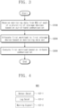
- FIG. 3 is a flowchart illustrating an operating method of an electronic device according to an embodiment of the present disclosure.
- the BMC 113 may receive monitoring data from each of the MCUs 133, 153, and 173 of the plurality of storage devices, based on the out-of-band communication between the BMC 113 and the MCUs 133, 153, and 173 (S100).
- the processor 111 may allocate a first workload among one or more workloads to a first storage device (e.g., one of 130, 150, and 170) among the plurality of storage devices 130, 150, and 170, based on a monitoring data set including a plurality of monitoring data (S200).
- the monitoring data set may refer to data that are obtained by integrating some or all of the pieces of monitoring data transmitted from the MCUs 133, 153, and 173.
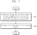
- a processor of a host device may determine a storage device having the lowest internal temperature from among a plurality of storage devices as a first storage device by using a monitoring data set (S201).
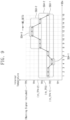
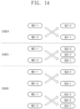
- the monitoring data sets MD_SET1, MD_SET2, and MD_SET3 may be respectively generated at different points in time by a BMC of a host device.
- an arbitrary storage device among storage devices included in the storage group SG3-1 may be determined as the first storage device, or another storage device selected by using any other hardware characteristics together with the internal temperature from among the storage devices included in the storage group SG3-1 may be determined as the first storage device.
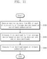
- FIG. 11 is a flowchart illustrating an operating method of an electronic device according to an embodiment of the present disclosure.
- the MCU (each of 133, 153, and 173) of the plurality of storage devices 130, 150, and 170 may transmit monitoring data to the BMC 113, based on the out-of-band communication between the BMC 113 and the MCUs 133, 153, and 173 (S100).
- the first storage device may execute the first workload, based on the in-band communication between the processor 111 and a storage controller (e.g., a storage controller included in the first storage device) (S300).
- a storage controller e.g., a storage controller included in the first storage device
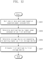
- FIG. 12 is a flowchart illustrating an embodiment of an operation of FIG. 11 , in which a first workload is allocated to a first storage device.
- the expected power consumption may be estimated based on requests and addresses (or requests, addresses, and pieces of data) included in each of the one or more workloads or based on past histories of external electronic devices transmitting execution requests associated with the one or more workloads to a host device.
- the process of estimating the expected power consumption will be described with reference to FIG. 13 .
- the processor 111 may further determine a second workload among the one or more workloads, may further determine a second storage device among the plurality of storage devices, and may allocate the second workload to the second storage device. For example, based on the result of the sorting in operation S231, the processor 111 may determine a workload having the lowest power consumption from among the one or more workloads as the first workload and may determine a workload having the highest power consumption from among the one or more workloads as the second workload. For example, the processor 111 may classify the one or more workloads into one or more workload groups based on the result of the sorting. Based on the workload groups, the processor 111 may determine a workload having the lowest power consumption as the first workload and may determine a workload having the highest power consumption as the second workload. The process of determining the first workload and the second workload will be described with reference to FIG. 13 .
- the processor 111 may estimate the expected power consumptions based on types of requests included in each of the one or more workloads, ranges of addresses included therein, or sizes of data included therein. For example, as requests included in one workload include more erase requests or more program requests, as ranges of addresses included in the one workload become greater, or as sizes of data included in the one workload become larger, the expected power consumption of the one workload may be estimated as a greater value.
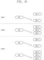
- the processor 111 may estimate that expected power consumptions of the one or more workloads WL1 to WL10 are 100, 30, 30, 20, 40, 40, 60, 80, 50, 20, respectively, and may sort the one or more workloads WL1 to WL10 based on the estimated expected power consumptions.
- the processor 111 may dynamically set a threshold power consumption based on the estimated expected power consumptions and may classify the one or more workloads WL1 to WL10 into groups WG1-1 and WG1-2 based on the threshold power consumption.
- the processor 111 may set, as the threshold power consumption, a power consumption (e.g., th_CP) between the highest expected power consumption (e.g., 100) and the lowest expected power consumption (e.g., 20) among the expected power consumptions that the one or more workloads WL1 to WL10 indicate.
- the processor 111 may classify workloads (e.g., WL1, WL8, WL7, and WL9) having a higher power consumption than the threshold power consumption as the workload group WG1-1 and may classify workloads (e.g., WL5, WL6, WL2, WL3, WL4, and WL10) having a lower power consumption than the threshold power consumption as the workload group WG1-2.
- the processor 111 may, in advance, set one or more threshold power consumptions and may classify the one or more workloads WL1 to WL10 into workload groups based on the one or more threshold power consumptions.
- a first workload, a second workload, a first storage device, and a second storage device may be determined based on the storage groups SG1-1, SG1-2, SG2-1, SG2-2, SG2-3, SG3-1, SG3-2, SG4-1, SG4-2, and SG4-3 of FIGS. 8 and 9 and the workload groups WG1-1 and WG1-2 of FIG. 13 .
- the workload group WG1-1 including workloads having a relatively high power consumption may be selected from the workload groups WG1-1 and WG1-2, and the storage group SG1-1 including storage devices having a relatively low internal temperature may be selected from the storage groups SG1-1 and SG1-2.
- any one of the workloads included in the workload group WG1-1 may be determined as the first workload, and any one of the storage devices included in the storage group SG1-1 may be determined as the first storage device.
- the present disclosure is not limited thereto.
- another storage device among the storage devices included in the storage group SG1-1 may be selected as the first storage device by using any other hardware characteristics together with an internal temperature.
- any one of the workloads included in the workload group WG1-2 may be determined as the second workload, and any one of the storage devices included in the storage group SG1-2 may be determined as the second storage device.
- the present disclosure is not limited thereto.
- another storage device among the storage devices included in the storage group SG1-2 may be selected as the second storage device by using any other hardware characteristics together with an internal temperature.
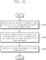
- the MCU (each of 133, 153, and 173) of the plurality of storage devices 130, 150, and 170 transmit monitoring data to the BMC 113, based on the out-of-band communication between the BMC 113 and the MCUs 133, 153, and 173 (S100).
- the processor 111 may insert a first workload among one or more workloads into a first workload queue among the one or more workload queues 115 and may allocate the first workload to a first storage device (e.g., one of 130, 150, and 170) among the plurality of storage devices 130, 150, and 170 (S250).
- the monitoring data set may refer to data that are obtained by integrating pieces of monitoring data respectively transmitted from the MCUs 133, 153, and 173.
- the first storage device may execute the first workload, based on the in-band communication between the processor 111 and a storage controller (e.g., a storage controller included in the first storage device) (S300).
- a storage controller e.g., a storage controller included in the first storage device
- FIGS. 16 and 17 are diagrams for describing an embodiment of workload queues of FIG. 15 .
- FIG. 18 is a diagram for describing an embodiment of a workload of FIG. 17 .
- a processor 510, one or more workload queues 531, 533, 535, and 537, and storage devices 551, 553, 555, and 557 are illustrated in FIG. 16
- the processor 510, one or more workload queues 531a, 533a, 535a, and 537a, and the storage devices 551, 553, 555, and 557 are illustrated in FIG. 17 .
- the processor 510 and the storage devices 551, 553, 555, and 557 may respectively correspond to the processor 111 and the storage devices 130, 150, and 170 of FIG. 1 , and the one or more workload queues 531, 533, 535, and 537 and the one or more workload queues 531a, 533a, 535a, and 537a may correspond to the workload queues 115.
- a host device may include the processor 510 and the one or more workload queues 531, 533, 535, and 537, and the processor 510 may include one or more cores 511, 513, 515, and 517.
- the one or more workload queues 531, 533, 535, and 537 may be generated to correspond to the one or more cores 511, 513, 515, and 517, respectively, and the number of one or more workload queues 531, 533, 535, and 537 may be equal to the number of one or more cores 511, 513, 515, and 517.
- the one or more workload queues 531, 533, 535, and 537 may be respectively dedicated for the storage devices 551, 553, 555, and 557.
- the storage devices 551, 553, 555, and 557 may respectively correspond to the one or more workload queues 531, 533, 535, and 537, and the number of one or more workload queues 531, 533, 535, and 537 may be equal to the number of storage devices 551, 553, 555, and 557.
- the processor 510 may insert a first workload into a first workload queue and allocates the first workload to a first storage device.
- the core 511 may insert the workload WLa into the workload queue 531 to allocate the workload WLa to the storage device 551
- the core 513 may insert the workload WLb into the workload queue 533 to allocate the workload WLb to the storage device 553.
- the core 515 may insert the workload WLc into the workload queue 535 to allocate the workload WLc to the storage device 555
- the core 517 may insert the workload WLd into the workload queue 537 to allocate the workload WLd to the storage device 557.
- storage devices may not respectively correspond to one or more workload queues, and the number of the storage devices may be more than the number of the one or more workload queues 531, 533, 535, and 537.
- the processor 510 may classify storage devices into one or more storage groups, and the number of the storage groups may be equal to the number of the one or more workload queues 531, 533, 535, and 537.
- the processor 510 may sort the one or more workload queues 531, 533, 535, and 537 in the order of workload size, based on one or more of an access frequency and a priority for each workload queue.
- the access frequency may increase.
- the one or more workload queues 531, 533, 535, and 537 may respectively correspond to external electronic devices transmitting the one or more workloads, and a priority of each of the workload queues 531, 533, 535, and 537 may be determined based on past histories of previous workloads transmitted by the external electronic devices.
- the one or more workload queues 531a, 533a, 535a, and 537a are not dedicated for the storage devices 551, 553, 555, and 557.
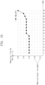
- a monitoring data set MD_SET4 including pieces of monitoring data is illustrated in FIG. 19 .
- the y-axis represents a remaining lifetime/reliability (e.g., as indicated by LT1, LT2, LT3, LT4, and LT5) and the x-axis represents storage devices SD1, SD2, SD3, SD4, SD5, SD6, SD7, SD8, SD9, SD10, SD11, SD12, SD13, SD14, SD15, and SD16 (e.g., SDx corresponds to these storage devices).
- the processor of the host device may dynamically set a threshold remaining lifetime/reliability based on the monitoring data set MD_SET4 and may classify storage devices into storage groups based on the threshold remaining lifetime/reliability.
- the processor of the host device may, in advance, set one or more threshold remaining lifetimes/reliabilities regardless of the monitoring data set MD_SET4 and may classify storage devices into storage groups based on the threshold remaining lifetimes/reliabilities.
- the processor of the host device may determine the first storage device for allocating an arbitrary workload based on the storage groups.
- an electronic system 1000 may include a host device 1010, a compute express link (CXL) storage device 1100, and a CXL memory device 1200 that communicate through a CXL switch SW_CXL.
- the host device 1010 and the CXL storage device 1100 may respectively correspond to the host device 110 and the storage device 130 of FIG. 1 .
- the host device 1010 may include a CXL host interface circuit 1010a.
- the CXL host interface circuit 1010a may include workload queues (e.g., 115 of FIG. 1 or 115a of FIG. 2 ).
- the CXL host interface circuit 1010a may communicate with the CXL storage device 1100 or the CXL memory device 1200 through the CXL switch SW_CXL.
- the CXL storage controller may store data in the non-volatile memory NVM or may transmit data present in the non-volatile memory NVM to the host device 1010.
- the non-volatile memory NVM may be a NAND flash memory, but the present disclosure is not limited thereto.
- the internal buffer memory iBFM may temporarily store data that are input to the CXL storage controller or are output from the CXL storage controller.
- the CXL memory device 1200 may store data in the buffer memory BFM or may send data stored in the buffer memory BFM to the host device 1010.
- the CXL memory device 1200 may store monitoring data associated with the CXL storage device 1100 in the buffer memory BFM and may transmit the monitoring data to the host device 1010 periodically or non-periodically.
- the buffer memory BFM may be a DRAM, but the present disclosure is not limited thereto.
- the host device 1010, the CXL storage device 1100, and the CXL memory device 1200 may be configured to share the same interface.
- the host device 1010, the CXL storage device 1100, and the CXL memory device 1200 may communicate with each other through the CXL switch SW_CXL.
- the CXL switch SW_CXL may refer to a low-latency and high-bandwidth link that supports coherency, memory access, and dynamic protocol muxing of IO protocols such that various connections between accelerators, memory devices, or various electronic devices may be implemented.
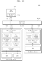
- the numbers of processors 3210 and memories 3220 included in the storage server 3200 may be variously selected.
- the processor 3210 and the memory 3220 may provide a processor-memory pair.
- the number of processors 3210 may be different from the number of memories 3220.
- the processor 3210 may include a single-core processor or a multi-core processor.
- the above description of the storage server 3200 may be similarly applied to the application server 3100.
- the application server 3100 does not include a storage device 3150.
- the storage server 3200 may include at least one storage device 3250.
- the number of storage devices 3250 included in the storage server 3200 may be variously selected according to embodiments.
- the application servers 3100 to 3100n may communicate with the storage servers 3200 to 3200m through a network 3300.
- the network 3300 may be implemented by using, for example, a fiber channel (FC) or Ethernet.
- the FC may be a medium used for relatively high-speed data transmission and may use an optical switch with high performance and high availability.
- the storage servers 3200 to 3200m may be provided as, for example, file storages, block storages, or object storages according to an access method of the network 3300.
- the network 3300 may be a storage-dedicated network, such as a storage area network (SAN).
- the SAN may be an FC-SAN, which uses an FC network and is implemented according to an FC protocol (FCP).
- FCP FC protocol
- the SAN may be an Internet protocol (IP)-SAN, which uses a transmission control protocol (TCP)/IP network and is implemented according to a SCSI over TCP/IP or Internet SCSI (iSCSI) protocol.
- IP Internet protocol
- TCP transmission control protocol
- iSCSI Internet SCSI
- the network 3300 may be a general network, such as a TCP/IP network.
- the network 3300 may be implemented according to a protocol, such as, for example, FC over Ethernet (FCoE), network attached storage (NAS), and NVMe over Fabrics (NVMe-oF).
- FCoE FC over Ethernet
- NAS network attached storage
- NVMe over Fabrics NVMe over Fabrics
- the application server 3100 may store data, which is requested by a user or a client to be stored, in one of the storage servers 3200 to 3200m through the network 3300. Also, the application server 3100 may obtain data, which is requested by the user or the client to be read, from one of the storage servers 3200 to 3200m through the network 3300.
- the application server 3100 may be implemented as a web server or a database management system (DBMS).
- DBMS database management system
- the application server 3100 may access a memory 3120n or a storage device 3150n, which is included in another application server 3100n, through the network 3300.
- the application server 3100 may access memories 3220 to 3220m or storage devices 3250 to 3250m, which are included in the storage servers 3200 to 3200m, through the network 3300.
- the application server 3100 may perform various operations on data stored in application servers 3100 to 3100n and/or the storage servers 3200 to 3200m.
- the application server 3100 may execute an instruction for moving or copying data between the application servers 3100 to 3100n and/or the storage servers 3200 to 3200m.
Landscapes
- Engineering & Computer Science (AREA)
- Theoretical Computer Science (AREA)
- Human Computer Interaction (AREA)
- Physics & Mathematics (AREA)
- General Engineering & Computer Science (AREA)
- General Physics & Mathematics (AREA)
- Computer Networks & Wireless Communication (AREA)
- Debugging And Monitoring (AREA)
Applications Claiming Priority (2)
| Application Number | Priority Date | Filing Date | Title |
|---|---|---|---|
| KR1020230002194A KR20240110284A (ko) | 2023-01-06 | 2023-01-06 | 전자 장치 및 이의 동작 방법 |
| US18/484,000 US12277328B2 (en) | 2023-01-06 | 2023-10-10 | Electronic device and operating method thereof |
Publications (1)
| Publication Number | Publication Date |
|---|---|
| EP4398085A1 true EP4398085A1 (fr) | 2024-07-10 |
Family
ID=88837360
Family Applications (1)
| Application Number | Title | Priority Date | Filing Date |
|---|---|---|---|
| EP23210046.1A Pending EP4398085A1 (fr) | 2023-01-06 | 2023-11-15 | Dispositif électronique et son procédé de fonctionnement |
Country Status (1)
| Country | Link |
|---|---|
| EP (1) | EP4398085A1 (fr) |
Cited By (1)
| Publication number | Priority date | Publication date | Assignee | Title |
|---|---|---|---|---|
| CN121116762A (zh) * | 2025-11-10 | 2025-12-12 | 苏州元脑智能科技有限公司 | 基板管理控制器的告警控制方法及装置 |
Citations (5)
| Publication number | Priority date | Publication date | Assignee | Title |
|---|---|---|---|---|
| US20190018600A1 (en) * | 2016-01-13 | 2019-01-17 | Hewlett Packard Enterprise Development Lp | Restructured input/output requests |
| US20200012452A1 (en) * | 2018-07-05 | 2020-01-09 | Hewlett Packard Enterprise Development Lp | Identification of substitute controllers based on temperature data |
| US20210182166A1 (en) * | 2019-12-12 | 2021-06-17 | Western Digital Technologies, Inc. | Zoned namespace management of non-volatile storage devices |
| US20210373951A1 (en) * | 2020-05-28 | 2021-12-02 | Samsung Electronics Co., Ltd. | Systems and methods for composable coherent devices |
| WO2022043812A1 (fr) * | 2020-08-26 | 2022-03-03 | International Business Machines Corporation | Équilibrage de charge de stockage |
-
2023
- 2023-11-15 EP EP23210046.1A patent/EP4398085A1/fr active Pending
Patent Citations (5)
| Publication number | Priority date | Publication date | Assignee | Title |
|---|---|---|---|---|
| US20190018600A1 (en) * | 2016-01-13 | 2019-01-17 | Hewlett Packard Enterprise Development Lp | Restructured input/output requests |
| US20200012452A1 (en) * | 2018-07-05 | 2020-01-09 | Hewlett Packard Enterprise Development Lp | Identification of substitute controllers based on temperature data |
| US20210182166A1 (en) * | 2019-12-12 | 2021-06-17 | Western Digital Technologies, Inc. | Zoned namespace management of non-volatile storage devices |
| US20210373951A1 (en) * | 2020-05-28 | 2021-12-02 | Samsung Electronics Co., Ltd. | Systems and methods for composable coherent devices |
| WO2022043812A1 (fr) * | 2020-08-26 | 2022-03-03 | International Business Machines Corporation | Équilibrage de charge de stockage |
Cited By (1)
| Publication number | Priority date | Publication date | Assignee | Title |
|---|---|---|---|---|
| CN121116762A (zh) * | 2025-11-10 | 2025-12-12 | 苏州元脑智能科技有限公司 | 基板管理控制器的告警控制方法及装置 |
Similar Documents
| Publication | Publication Date | Title |
|---|---|---|
| US12277328B2 (en) | Electronic device and operating method thereof | |
| US20160320971A1 (en) | Memory System and Method for Differential Thermal Throttling | |
| CN112148525A (zh) | 实现更快且经过调节的装置初始化时间 | |
| US12235713B2 (en) | Method for operating storage device and host device, and storage device | |
| US12112045B2 (en) | Storage device and method of operating the same | |
| US20190108892A1 (en) | System and Method for Post-Package Repair Across DRAM Banks and Bank Groups | |
| US10013173B2 (en) | Data storage device with command buffer management module and method of operating same | |
| US20160291869A1 (en) | Data storage device and data processing system including the same | |
| CN116136743A (zh) | 存储设备的操作方法及存储系统的操作方法 | |
| US10747660B2 (en) | Method and system for forming and using memory superblocks based on performance grades | |
| US12525285B2 (en) | Storage controller with improved write amplification characteristics and storage device including the same | |
| US12282422B2 (en) | Storage device and operating method thereof | |
| EP4521236B1 (fr) | Dispositif de stockage et dispositif hôte | |
| EP4398085A1 (fr) | Dispositif électronique et son procédé de fonctionnement | |
| US20250224902A1 (en) | Computational storage device, method for operating the computational storage device and method for operating host device | |
| US20250231688A1 (en) | Method of operating memory system and memory system performing the same | |
| US20250165155A1 (en) | System and method for memory bad block management | |
| KR102856778B1 (ko) | 서치 회로 및 컨트롤러 | |
| US20240069814A1 (en) | Storage server and operation method of storage server | |
| US20230325093A1 (en) | Storage device and operating method thereof | |
| EP4332773A1 (fr) | Serveur de stockage et procédé de fonctionnement d'un serveur de stockage | |
| US12306774B2 (en) | Computational storage device and method of operating the same | |
| US20250053471A1 (en) | Storage systems including host and storage devices and methods of operating the same | |
| US12217797B2 (en) | Storage device and operating method thereof | |
| US12561084B2 (en) | Computational storage device configured to transfer intermediate data between compute engines and method for operating the device |
Legal Events
| Date | Code | Title | Description |
|---|---|---|---|
| PUAI | Public reference made under article 153(3) epc to a published international application that has entered the european phase |
Free format text: ORIGINAL CODE: 0009012 |
|
| STAA | Information on the status of an ep patent application or granted ep patent |
Free format text: STATUS: THE APPLICATION HAS BEEN PUBLISHED |
|
| AK | Designated contracting states |
Kind code of ref document: A1 Designated state(s): AL AT BE BG CH CY CZ DE DK EE ES FI FR GB GR HR HU IE IS IT LI LT LU LV MC ME MK MT NL NO PL PT RO RS SE SI SK SM TR |
|
| STAA | Information on the status of an ep patent application or granted ep patent |
Free format text: STATUS: REQUEST FOR EXAMINATION WAS MADE |
|
| P01 | Opt-out of the competence of the unified patent court (upc) registered |
Free format text: CASE NUMBER: APP_66051/2024 Effective date: 20241213 |
|
| 17P | Request for examination filed |
Effective date: 20250102 |
|
| STAA | Information on the status of an ep patent application or granted ep patent |
Free format text: STATUS: EXAMINATION IS IN PROGRESS |
|
| 17Q | First examination report despatched |
Effective date: 20250306 |